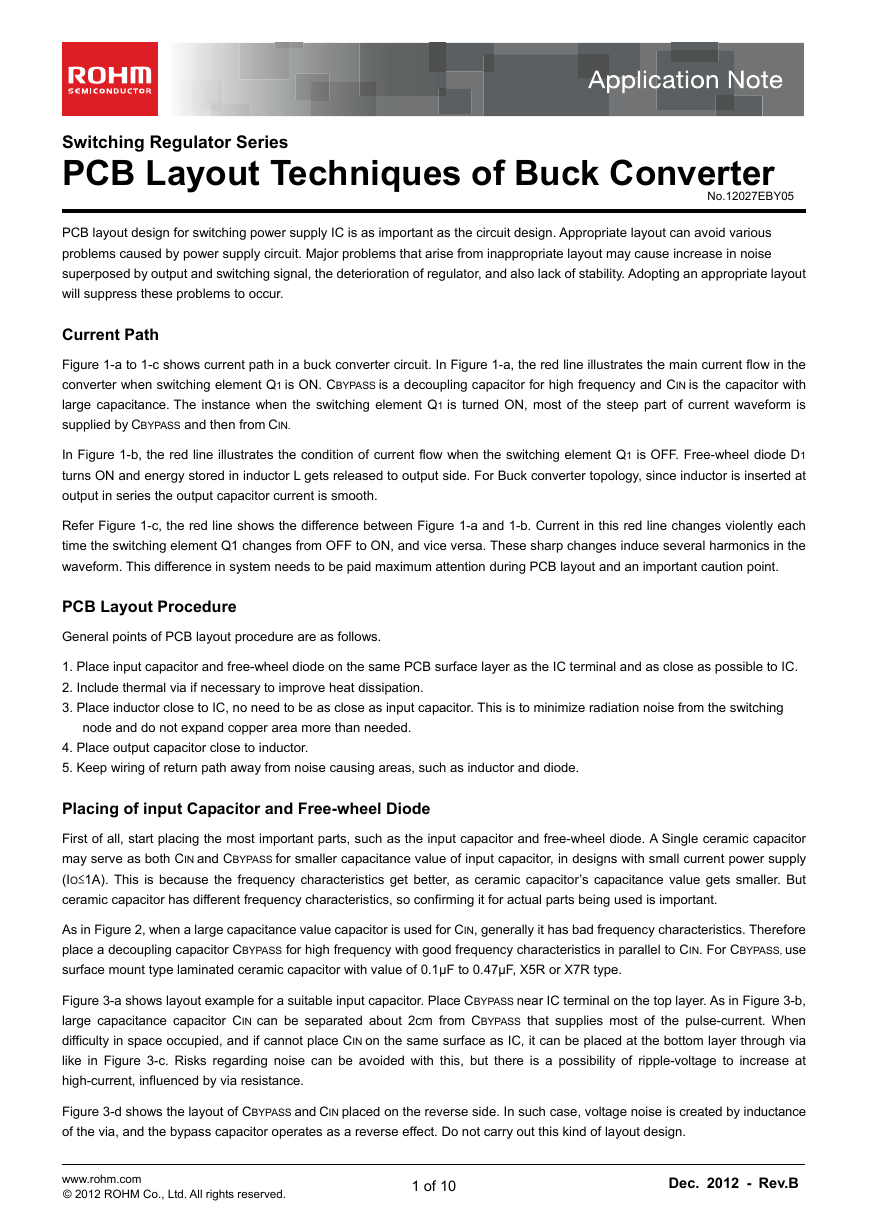
Switching Regulator Series
PCB Layout Techniques of Buck Converter
No.12027EBY05
PCB layout design for switching power supply IC is as important as the circuit design. Appropriate layout can avoid various
problems caused by power supply circuit. Major problems that arise from inappropriate layout may cause increase in noise
superposed by output and switching signal, the deterioration of regulator, and also lack of stability. Adopting an appropriate layout
will suppress these problems to occur.
Current Path
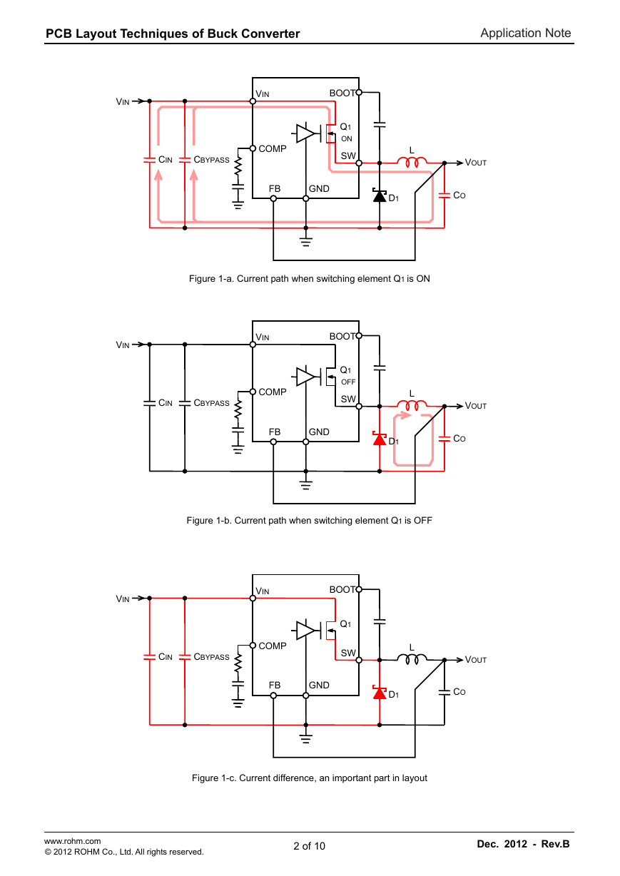
Figure 1-a to 1-c shows current path in a buck converter circuit. In Figure 1-a, the red line illustrates the main current flow in the
converter when switching element Q1 is ON. CBYPASS is a decoupling capacitor for high frequency and CIN is the capacitor with
large capacitance. The instance when the switching element Q1 is turned ON, most of the steep part of current waveform is
supplied by CBYPASS and then from CIN.
In Figure 1-b, the red line illustrates the condition of current flow when the switching element Q1 is OFF. Free-wheel diode D1
turns ON and energy stored in inductor L gets released to output side. For Buck converter topology, since inductor is inserted at
output in series the output capacitor current is smooth.
Refer Figure 1-c, the red line shows the difference between Figure 1-a and 1-b. Current in this red line changes violently each
time the switching element Q1 changes from OFF to ON, and vice versa. These sharp changes induce several harmonics in the
waveform. This difference in system needs to be paid maximum attention during PCB layout and an important caution point.
PCB Layout Procedure
General points of PCB layout procedure are as follows.
1. Place input capacitor and free-wheel diode on the same PCB surface layer as the IC terminal and as close as possible to IC.
2. Include thermal via if necessary to improve heat dissipation.
3. Place inductor close to IC, no need to be as close as input capacitor. This is to minimize radiation noise from the switching
node and do not expand copper area more than needed.
4. Place output capacitor close to inductor.
5. Keep wiring of return path away from noise causing areas, such as inductor and diode.
Placing of input Capacitor and Free-wheel Diode
First of all, start placing the most important parts, such as the input capacitor and free-wheel diode. A Single ceramic capacitor
may serve as both CIN and CBYPASS for smaller capacitance value of input capacitor, in designs with small current power supply
(IO≤1A). This is because the frequency characteristics get better, as ceramic capacitor’s capacitance value gets smaller. But
ceramic capacitor has different frequency characteristics, so confirming it for actual parts being used is important.
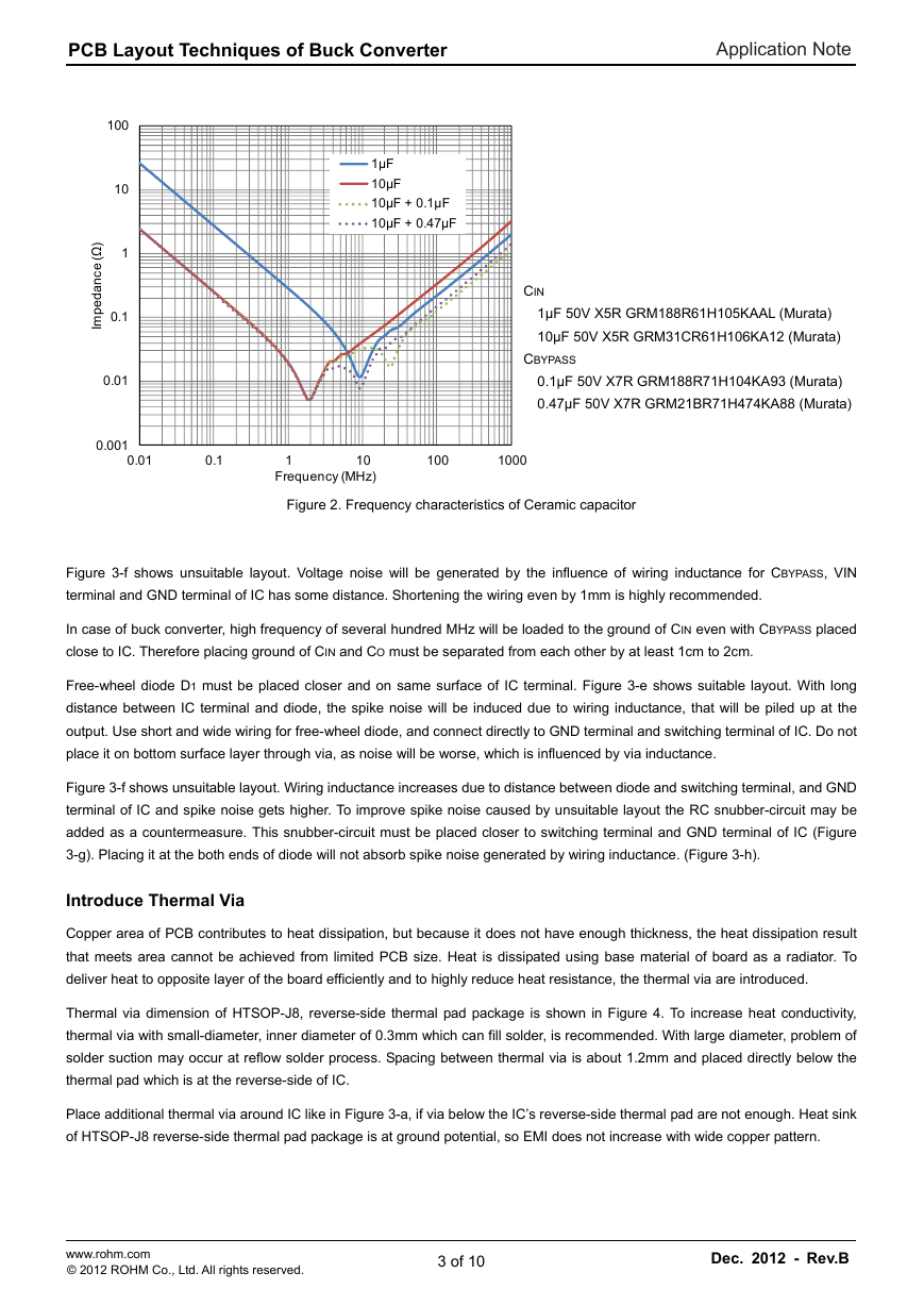
As in Figure 2, when a large capacitance value capacitor is used for CIN, generally it has bad frequency characteristics. Therefore
place a decoupling capacitor CBYPASS for high frequency with good frequency characteristics in parallel to CIN. For CBYPASS, use
surface mount type laminated ceramic capacitor with value of 0.1µF to 0.47µF, X5R or X7R type.
Figure 3-a shows layout example for a suitable input capacitor. Place CBYPASS near IC terminal on the top layer. As in Figure 3-b,
large capacitance capacitor CIN can be separated about 2cm from CBYPASS that supplies most of the pulse-current. When
difficulty in space occupied, and if cannot place CIN on the same surface as IC, it can be placed at the bottom layer through via
like in Figure 3-c. Risks regarding noise can be avoided with this, but there is a possibility of ripple-voltage to increase at
high-current, influenced by via resistance.
Figure 3-d shows the layout of CBYPASS and CIN placed on the reverse side. In such case, voltage noise is created by inductance
of the via, and the bypass capacitor operates as a reverse effect. Do not carry out this kind of layout design.
www.rohm.com
© 2012 ROHM Co., Ltd. All rights reserved.
1 of 10
Dec. 2012 - Rev.B
�
PCB Layout Techniques of Buck Converter
Application Note
VIN
VIN
BOOT
CIN
CBYPASS
COMP
Q1
ON
SW
L
VOUT
FB
GND
D1
CO
Figure 1-a. Current path when switching element Q1 is ON
VIN
VIN
BOOT
CIN
CBYPASS
COMP
Q1
OFF
SW
L
VOUT
FB
GND
D1
CO
Figure 1-b. Current path when switching element Q1 is OFF
VIN
VIN
BOOT
CIN
CBYPASS
COMP
Q1
SW
L
VOUT
FB
GND
D1
CO
Figure 1-c. Current difference, an important part in layout
www.rohm.com
© 2012 ROHM Co., Ltd. All rights reserved.
2 of 10
Dec. 2012 - Rev.B
�
PCB Layout Techniques of Buck Converter
Application Note
100
10
1
0.1
1µF
10µF
10µF + 0.1µF
10µF + 0.47µF
)
Ω
(
e
c
n
a
d
e
p
m
I
0.01
0.001
0.01
CIN
1µF 50V X5R GRM188R61H105KAAL (Murata)
10µF 50V X5R GRM31CR61H106KA12 (Murata)
CBYPASS
0.1µF 50V X7R GRM188R71H104KA93 (Murata)
0.47µF 50V X7R GRM21BR71H474KA88 (Murata)
0.1
1
10
Frequency (MHz)
100
1000
Figure 2. Frequency characteristics of Ceramic capacitor
Figure 3-f shows unsuitable layout. Voltage noise will be generated by the influence of wiring inductance for CBYPASS, VIN
terminal and GND terminal of IC has some distance. Shortening the wiring even by 1mm is highly recommended.
In case of buck converter, high frequency of several hundred MHz will be loaded to the ground of CIN even with CBYPASS placed
close to IC. Therefore placing ground of CIN and CO must be separated from each other by at least 1cm to 2cm.
Free-wheel diode D1 must be placed closer and on same surface of IC terminal. Figure 3-e shows suitable layout. With long
distance between IC terminal and diode, the spike noise will be induced due to wiring inductance, that will be piled up at the
output. Use short and wide wiring for free-wheel diode, and connect directly to GND terminal and switching terminal of IC. Do not
place it on bottom surface layer through via, as noise will be worse, which is influenced by via inductance.
Figure 3-f shows unsuitable layout. Wiring inductance increases due to distance between diode and switching terminal, and GND
terminal of IC and spike noise gets higher. To improve spike noise caused by unsuitable layout the RC snubber-circuit may be
added as a countermeasure. This snubber-circuit must be placed closer to switching terminal and GND terminal of IC (Figure
3-g). Placing it at the both ends of diode will not absorb spike noise generated by wiring inductance. (Figure 3-h).
Introduce Thermal Via
Copper area of PCB contributes to heat dissipation, but because it does not have enough thickness, the heat dissipation result
that meets area cannot be achieved from limited PCB size. Heat is dissipated using base material of board as a radiator. To
deliver heat to opposite layer of the board efficiently and to highly reduce heat resistance, the thermal via are introduced.
Thermal via dimension of HTSOP-J8, reverse-side thermal pad package is shown in Figure 4. To increase heat conductivity,
thermal via with small-diameter, inner diameter of 0.3mm which can fill solder, is recommended. With large diameter, problem of
solder suction may occur at reflow solder process. Spacing between thermal via is about 1.2mm and placed directly below the
thermal pad which is at the reverse-side of IC.
Place additional thermal via around IC like in Figure 3-a, if via below the IC’s reverse-side thermal pad are not enough. Heat sink
of HTSOP-J8 reverse-side thermal pad package is at ground potential, so EMI does not increase with wide copper pattern.
www.rohm.com
© 2012 ROHM Co., Ltd. All rights reserved.
3 of 10
Dec. 2012 - Rev.B
�
PCB Layout Techniques of Buck Converter
Application Note
GND
VOUT
CO
CO
GND
VIN
CIN
CBYPASS
EN
C5
T
O
O
B
N
E
C
N
Y
S
N
V
I
D
N
G
P
M
O
C
B
F
W
S
IC
C1
R3
2
R
1
R
D1
L
GND
VOUT
CO
CO
GND
CIN
VIN
EN
C5
CBYPASS
T
O
O
B
N
E
C
N
Y
S
N
V
I
D1
L
D
N
G
P
M
O
C
B
F
W
S
IC
C1
R3
2
R
1
R
Figure 3-a. Placement of suitable input capacitor
Figure 3-b. No problem with CIN separated about 2cm
when CBYPASS is closely placed on same surface
GND
VOUT
CO
CO
GND
VIN
EN
C5
CBYPASS
CIN
T
O
O
B
N
E
C
N
Y
S
N
V
I
D1
L
D
N
G
P
M
O
C
B
F
W
S
IC
C1
R3
2
R
1
R
Top Layer
Bottom Layer
CBYPASS
IC
CIN
GND
VOUT
CO
CO
GND
VIN
EN
C5
CBYPASS
CIN
T
O
O
B
N
E
C
N
Y
S
N
V
I
D1
L
D
N
G
P
M
O
C
B
F
W
S
IC
C1
R3
2
R
1
R
Top Layer
Bottom Layer
CIN
IC
CBYPASS
Figure 3-c. Increase of ripple voltage is concerned
when CIN is placed on bottom layer.
Figure 3-d. Unsuitable layout for input capacitor.
Noise increased by via inductance
GND
VOUT
CO
CO
GND
VIN
CIN
CBYPASS
EN
C5
T
O
O
B
N
E
C
N
Y
S
N
V
I
D
N
G
P
M
O
C
B
F
W
S
IC
C1
R3
2
R
1
R
D1
L
Figure 3-e. Suitable placement of free-wheel diode
GND
VIN
CIN
EN
C5
CBYPASS
D1
GND
VOUT
CO
CO
T
O
O
B
N
E
C
N
Y
S
N
V
I
D
N
G
P
M
O
C
B
F
W
S
IC
C1
R3
L
2
R
1
R
Figure 3-f. Unsuitable layout for diode
www.rohm.com
© 2012 ROHM Co., Ltd. All rights reserved.
4 of 10
Dec. 2012 - Rev.B
�
PCB Layout Techniques of Buck Converter
Application Note
GND
VIN
CIN
EN
C5
GND
VIN
CIN
EN
C5
CBYPASS
D1
GND
VOUT
CO
CO
T
O
O
B
N
E
C
N
Y
S
N
V
I
D
N
G
P
M
O
C
B
F
W
S
IC
C1
R3
L
2
R
1
R
GND
VOUT
CO
CO
CBYPASS
D1
T
O
O
B
N
E
C
N
Y
S
N
V
I
D
N
G
P
M
O
C
B
F
W
S
IC
C1
R3
L
2
R
1
R
Figure 3-g. Suitable placement of snubber circuit
Figure 3-h. Unsuitable placement of snubber circuit
Central land
Thermal via
Length D3
Width E3
Pitch
Diameter
4.90mm
3.20mm
1.20mm
φ0.30mm
Figure 4. Thermal via dimension of reverse side thermal pad package
Placing Inductor
Place inductor close to IC, no need to place it as close as the input capacitor, to minimize radiation noise from switching node,
and do not expand copper pattern area if not necessary. Increasing copper area is most likely to be thought of to improve wire
resistance and to cool down device, but enlarged area may work as an antenna and may lead to increase in EMI.
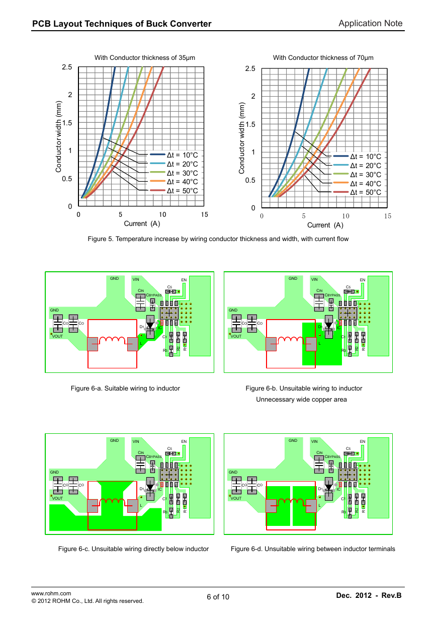
Permissible current flow is one of the guideline to determine wiring width. Figure 5 shows a graph of rising temperature due to
self-heating and conductor width when certain amount of current is flowing. For example, when 2A current is flowing through the
wire with conductor thickness of 35µm, keeping conductor width of 0.53mm is suitable to prevent temperature to rise by 20°C.
Wiring can be affected by heat from surrounding parts and surrounding temperature, therefore using conductor width with enough
margins is recommended. As an example, for 1 ounce (35µm) board conductor, width more than 1mm per 1A, and for 2 ounce
(70µm) board conductor, width more than 0.7mm per 1A is used for wiring.
Figure 6-a shows layout considering wiring area from EMI point of view. Also, unsuitable layout which has unnecessary wide
copper area is shown in Figure 6-b.
Not placing ground layer directly below the inductor (Figure 6-c) is also a point to pay attention to, when placing inductor. Due to
the eddy current occurring in the ground layer, the inductor value decreases and the loss increases (decrease of Q) with set-off
effect from line of magnetic force. Signal line other than ground also has the possibility of propagating switching noise caused by
eddy current. It is better to avoid wiring directly under inductor. If wiring is unavoidable, please use closed magnetic circuit
structured inductor with small leak from line of magnetic force.
www.rohm.com
© 2012 ROHM Co., Ltd. All rights reserved.
5 of 10
Dec. 2012 - Rev.B
�
PCB Layout Techniques of Buck Converter
Application Note
2.5
2
)
1.5
1
m
m
(
h
t
i
d
w
r
o
t
c
u
d
n
o
C
0.5
0
0
With Conductor thickness of 35µm With Conductor thickness of 70µm
2.5
2
)
1.5
1
m
m
(
h
t
i
d
w
r
o
t
c
u
d
n
o
C
0.5
0
0
Δt = 10°C
Δt = 20°C
Δt = 30°C
Δt = 40°C
Δt = 50°C
5
10
Current (A)
15
Δt = 10°C
Δt = 20°C
Δt = 30°C
Δt = 40°C
Δt = 50°C
5
10
Current (A)
15
Figure 5. Temperature increase by wiring conductor thickness and width, with current flow
GND
VOUT
CO
CO
GND
VIN
CIN
CBYPASS
EN
C5
T
O
O
B
N
E
C
N
Y
S
N
V
I
D
N
G
P
M
O
C
B
F
W
S
IC
C1
R3
2
R
1
R
D1
L
GND
VOUT
CO
CO
GND
VIN
CIN
CBYPASS
EN
C5
T
O
O
B
N
E
C
N
Y
S
N
V
I
D
N
G
P
M
O
C
B
F
W
S
IC
C1
R3
2
R
1
R
D1
L
Figure 6-a. Suitable wiring to inductor Figure 6-b. Unsuitable wiring to inductor
Unnecessary wide copper area
GND
VOUT
CO
CO
GND
VIN
CIN
CBYPASS
EN
C5
T
O
O
B
N
E
C
N
Y
S
N
V
I
D
N
G
P
M
O
C
B
F
W
S
IC
C1
R3
2
R
1
R
D1
L
GND
VOUT
CO
CO
GND
VIN
CIN
CBYPASS
EN
C5
T
O
O
B
N
E
C
N
Y
S
N
V
I
D
N
G
P
M
O
C
B
F
W
S
IC
C1
R3
2
R
1
R
D1
L
Figure 6-c. Unsuitable wiring directly below inductor Figure 6-d. Unsuitable wiring between inductor terminals
www.rohm.com
© 2012 ROHM Co., Ltd. All rights reserved.
6 of 10
Dec. 2012 - Rev.B
�
PCB Layout Techniques of Buck Converter
Application Note
Space between inductor terminals must also be paid attention. If distance between terminals are close like in Figure 6-d, high
frequency signal of switching node is induced to output through stray capacitance.
Place Output Capacitor Close to Inductor
Output current is smooth in buck converter as inductor is inserted to output in series. Place output capacitor close to inductor; no
need to place it as close as input capacitor. Because high frequency of several hundred MHz is loaded on ground of input, so
placing ground of CIN and CO 1cm to 2cm apart is recommended. If they are close to each other, high frequency noise of input
may be propagated to output through CO.
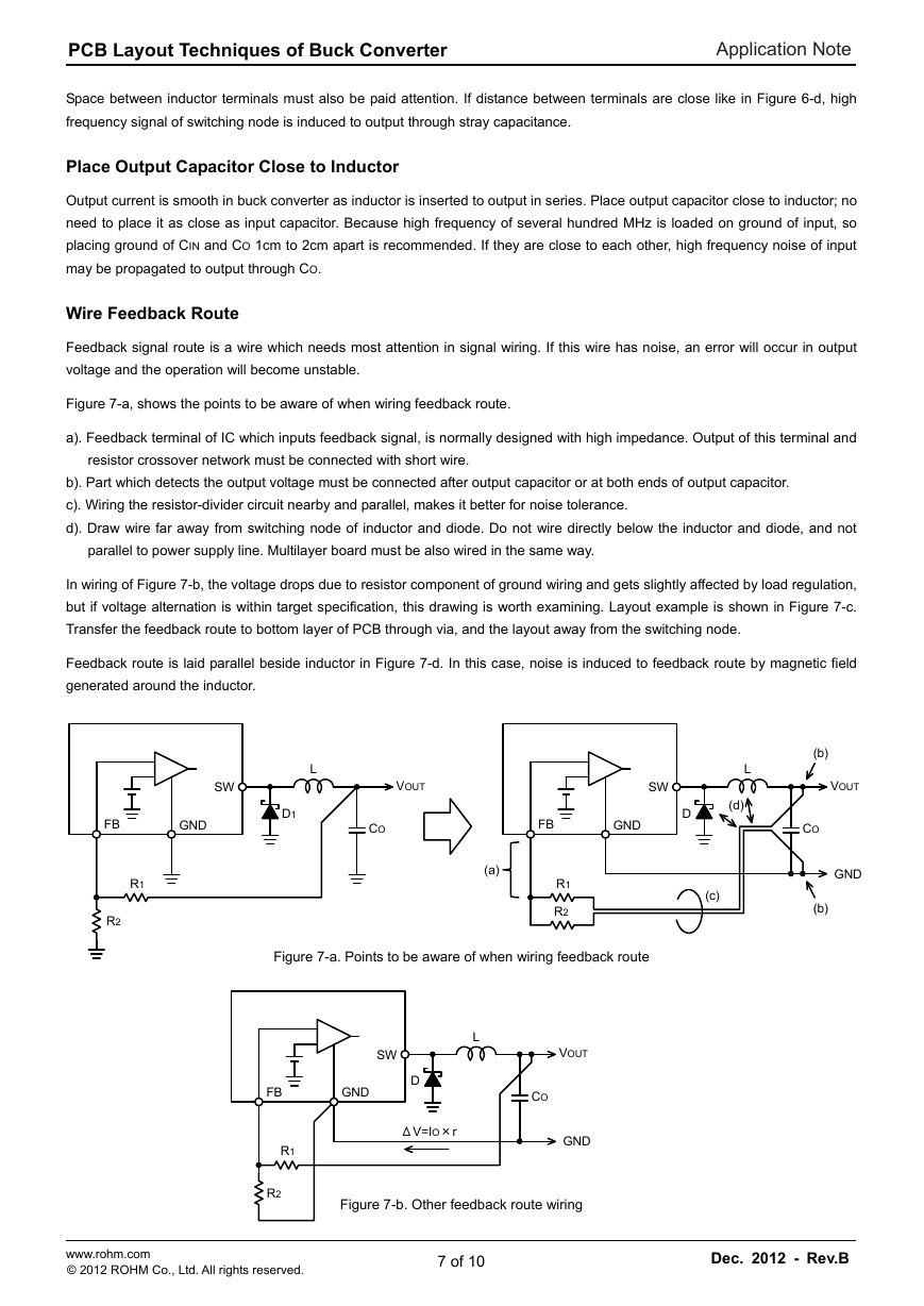
Wire Feedback Route
Feedback signal route is a wire which needs most attention in signal wiring. If this wire has noise, an error will occur in output
voltage and the operation will become unstable.
Figure 7-a, shows the points to be aware of when wiring feedback route.
a). Feedback terminal of IC which inputs feedback signal, is normally designed with high impedance. Output of this terminal and
resistor crossover network must be connected with short wire.
b). Part which detects the output voltage must be connected after output capacitor or at both ends of output capacitor.
c). Wiring the resistor-divider circuit nearby and parallel, makes it better for noise tolerance.
d). Draw wire far away from switching node of inductor and diode. Do not wire directly below the inductor and diode, and not
parallel to power supply line. Multilayer board must be also wired in the same way.
In wiring of Figure 7-b, the voltage drops due to resistor component of ground wiring and gets slightly affected by load regulation,
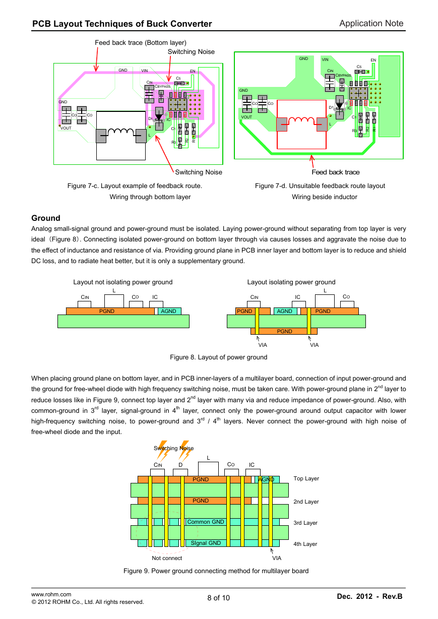
but if voltage alternation is within target specification, this drawing is worth examining. Layout example is shown in Figure 7-c.
Transfer the feedback route to bottom layer of PCB through via, and the layout away from the switching node.
Feedback route is laid parallel beside inductor in Figure 7-d. In this case, noise is induced to feedback route by magnetic field
generated around the inductor.
SW
L
D1
VOUT
CO
FB
GND
SW
D
L
(d)
FB
GND
R1
R2
(a)
R1
R2
(c)
Figure 7-a. Points to be aware of when wiring feedback route
(b)
VOUT
CO
GND
(b)
L
SW
D
ΔV=IO×r
CO
VOUT
GND
Figure 7-b. Other feedback route wiring
FB
GND
R1
R2
www.rohm.com
© 2012 ROHM Co., Ltd. All rights reserved.
7 of 10
Dec. 2012 - Rev.B
�
PCB Layout Techniques of Buck Converter
Application Note
Feed back trace (Bottom layer)
Switching Noise
GND
VOUT
CO
CO
GND
VIN
CIN
CBYPASS
EN
C5
T
O
O
B
N
E
C
N
Y
S
N
V
I
D
N
G
P
M
O
C
B
F
W
S
IC
C1
R3
2
R
1
R
D1
L
GND
VOUT
CO
CO
GND
VIN
CIN
CBYPASS
EN
C5
T
O
O
B
N
E
C
N
Y
S
N
V
I
P
M
O
C
D
N
G
B
F
W
S
IC
C1
R3
2
R
1
R
D1
L
Switching Noise
Feed back trace
Figure 7-c. Layout example of feedback route. Figure 7-d. Unsuitable feedback route layout
Wiring through bottom layer Wiring beside inductor
Ground
Analog small-signal ground and power-ground must be isolated. Laying power-ground without separating from top layer is very
ideal (Figure 8). Connecting isolated power-ground on bottom layer through via causes losses and aggravate the noise due to
the effect of inductance and resistance of via. Providing ground plane in PCB inner layer and bottom layer is to reduce and shield
DC loss, and to radiate heat better, but it is only a supplementary ground.
Layout not isolating power ground Layout isolating power ground
CIN
L
PGND
CO
IC
CIN
IC
L
CO
AGND
PGND
AGND
PGND
VIA
Figure 8. Layout of power ground
PGND
VIA
When placing ground plane on bottom layer, and in PCB inner-layers of a multilayer board, connection of input power-ground and
the ground for free-wheel diode with high frequency switching noise, must be taken care. With power-ground plane in 2nd layer to
reduce losses like in Figure 9, connect top layer and 2nd layer with many via and reduce impedance of power-ground. Also, with
common-ground in 3rd layer, signal-ground in 4th layer, connect only the power-ground around output capacitor with lower
high-frequency switching noise, to power-ground and 3rd / 4th layers. Never connect the power-ground with high noise of
free-wheel diode and the input.
Switching Noise
CIN
D
L
PGND
PGND
Common GND
SIgnal GND
CO
IC
AGND
Top Layer
2nd Layer
3rd Layer
4th Layer
Not connect
VIA
Figure 9. Power ground connecting method for multilayer board
www.rohm.com
© 2012 ROHM Co., Ltd. All rights reserved.
8 of 10
Dec. 2012 - Rev.B
�




 2023年江西萍乡中考道德与法治真题及答案.doc
 2012年重庆南川中考生物真题及答案.doc
 2013年江西师范大学地理学综合及文艺理论基础考研真题.doc
 2020年四川甘孜小升初语文真题及答案I卷.doc
 2020年注册岩土工程师专业基础考试真题及答案.doc
 2023-2024学年福建省厦门市九年级上学期数学月考试题及答案.doc
 2021-2022学年辽宁省沈阳市大东区九年级上学期语文期末试题及答案.doc
 2022-2023学年北京东城区初三第一学期物理期末试卷及答案.doc
 2018上半年江西教师资格初中地理学科知识与教学能力真题及答案.doc
 2012年河北国家公务员申论考试真题及答案-省级.doc
 2020-2021学年江苏省扬州市江都区邵樊片九年级上学期数学第一次质量检测试题及答案.doc
 2022下半年黑龙江教师资格证中学综合素质真题及答案.doc