A4988
DMOS Microstepping Driver with Translator
And Overcurrent Protection
Features and Benefits
▪ Low RDS(ON) outputs
▪ Automatic current decay mode detection/selection
▪ Mixed and Slow current decay modes
▪ Synchronous rectification for low power dissipation
▪ Internal UVLO
▪ Crossover-current protection
▪ 3.3 and 5 V compatible logic supply
▪ Thermal shutdown circuitry
▪ Short-to-ground protection
▪ Shorted load protection
▪ Five selectable step modes: full, 1/2, 1/4, 1/8, and 1/16
Package:
28-contact QFN
with exposed thermal pad
5 mm × 5 mm × 0.90 mm
(ET package)
Description
The A4988 is a complete microstepping motor driver with
built-in translator for easy operation. It is designed to operate
bipolar stepper motors in full-, half-, quarter-, eighth-, and
sixteenth-step modes, with an output drive capacity of up to
35 V and ±2 A. The A4988 includes a fixed off-time current
regulator which has the ability to operate in Slow or Mixed
decay modes.
The translator is the key to the easy implementation of the
A4988. Simply inputting one pulse on the STEP input drives
the motor one microstep. There are no phase sequence tables,
high frequency control lines, or complex interfaces to program.
The A4988 interface is an ideal fit for applications where a
complex microprocessor is unavailable or is overburdened.
During stepping operation, the chopping control in the A4988
automatically selects the current decay mode, Slow or Mixed.
In Mixed decay mode, the device is set initially to a fast decay
for a proportion of the fixed off-time, then to a slow decay for
the remainder of the off-time. Mixed decay current control
results in reduced audible motor noise, increased step accuracy,
and reduced power dissipation.
Approximate size
Continued on the next page…
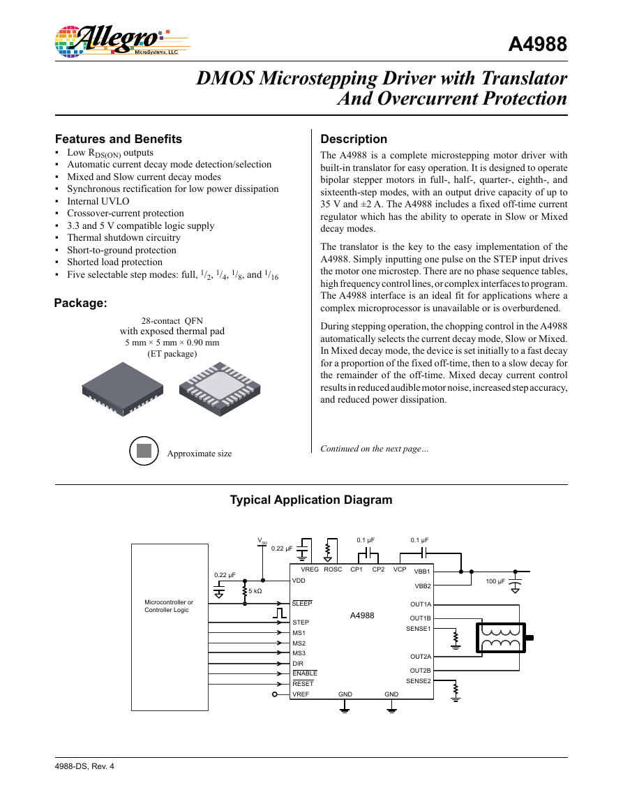
Typical Application Diagram
VDD
0.22 μF
0.1 μF
0.1 μF
0.22 μF
5 kΩ
Microcontroller or
Controller Logic
4988-DS, Rev. 4
VREG
ROSC
CP1
CP2
VCP
VBB1
VBB2
100 μF
VDD
SLEEP
STEP
MS1
MS2
MS3
DIR
ENABLE
RESET
VREF
A4988
OUT1A
OUT1B
SENSE1
OUT2A
OUT2B
SENSE2
GND
GND
�
A4988
DMOS Microstepping Driver with Translator
And Overcurrent Protection
Description (continued)
Internal synchronous rectification control circuitry is provided
to improve power dissipation during PWM operation. Internal
circuit protection includes: thermal shutdown with hysteresis,
undervoltage lockout (UVLO), and crossover-current protection.
Special power-on sequencing is not required.
The A4988 is supplied in a surface mount QFN package (ES), 5 mm
× 5 mm, with a nominal overall package height of 0.90 mm and an
exposed pad for enhanced thermal dissipation. It is lead (Pb) free
(suffix –T), with 100% matte tin plated leadframes.
Selection Guide
Part Number
A4988SETTR-T
28-contact QFN with exposed thermal pad
1500 pieces per 7-in. reel
Package
Packing
Absolute Maximum Ratings
Characteristic
Symbol
Notes
Rating
Units
Load Supply Voltage
Output Current
Logic Input Voltage
Logic Supply Voltage
Motor Outputs Voltage
Sense Voltage
Reference Voltage
Operating Ambient Temperature
Maximum Junction
Storage Temperature
VBB
IOUT
VIN
VDD
VSENSE
VREF
TA
TJ(max)
Tstg
Range S
35
±2
–0.3 to 5.5
–0.3 to 5.5
–2.0 to 37
–0.5 to 0.5
5.5
–20 to 85
150
–55 to 150
V
A
V
V
V
V
V
ºC
ºC
ºC
Allegro MicroSystems, LLC
115 Northeast Cutoff
Worcester, Massachusetts 01615-0036 U.S.A.
1.508.853.5000; www.allegromicro.com
2
�
A4988
DMOS Microstepping Driver with Translator
And Overcurrent Protection
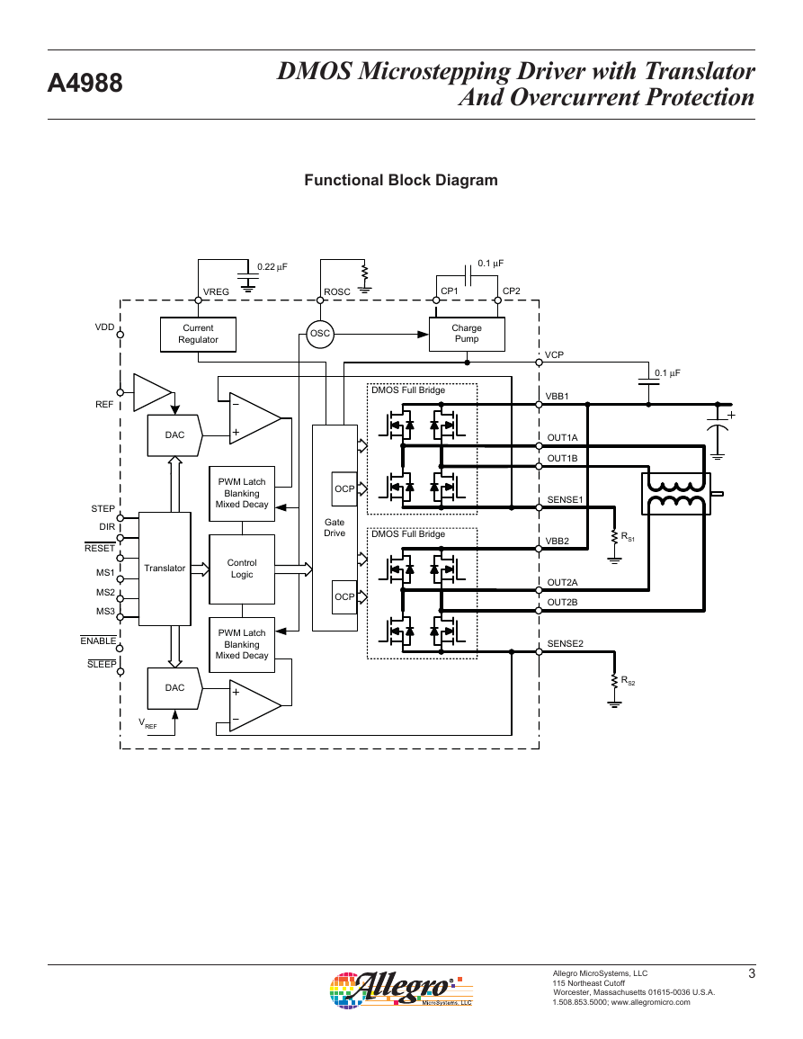
Functional Block Diagram
0.22 F
0.1 F
VREG
ROSC
CP1
CP2
Current
Regulator
OSC
Charge
Pump
DMOS Full Bridge
DMOS Full Bridge
OCP
Gate
Drive
OCP
DAC
PWM Latch
Blanking
Mixed Decay
Translator
Control
Logic
PWM Latch
Blanking
Mixed Decay
DAC
VREF
VDD
REF
STEP
DIR
RESET
MS1
MS2
MS3
ENABLE
SLEEP
VCP
VBB1
OUT1A
OUT1B
SENSE1
VBB2
OUT2A
OUT2B
SENSE2
0.1 F
RS1
RS2
Allegro MicroSystems, LLC
115 Northeast Cutoff
Worcester, Massachusetts 01615-0036 U.S.A.
1.508.853.5000; www.allegromicro.com
3
�
A4988
DMOS Microstepping Driver with Translator
And Overcurrent Protection
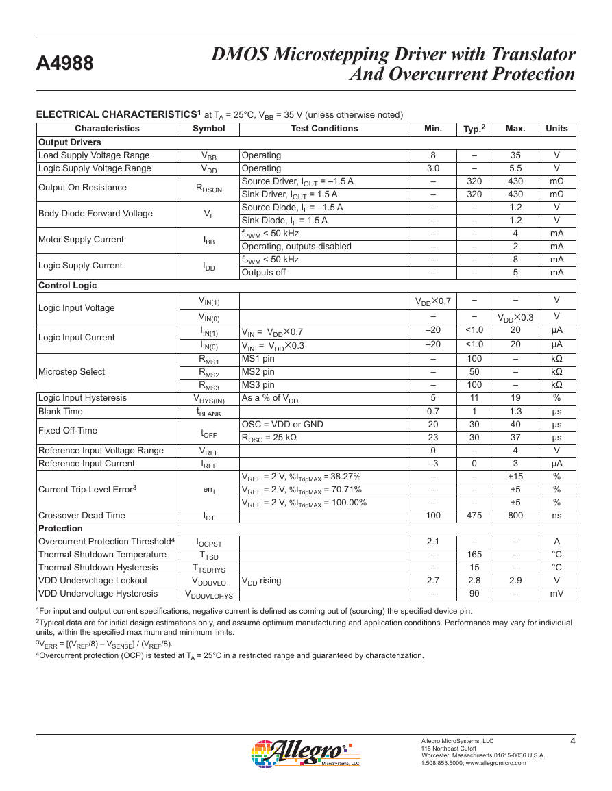
ELECTRICAL CHARACTERISTICS1 at TA = 25°C, VBB = 35 V (unless otherwise noted)
Test Conditions
Characteristics
Symbol
Output Drivers
Load Supply Voltage Range
Logic Supply Voltage Range
Output On Resistance
Body Diode Forward Voltage
Motor Supply Current
Logic Supply Current
Control Logic
Logic Input Voltage
Logic Input Current
Microstep Select
Logic Input Hysteresis
Blank Time
Fixed Off-Time
Reference Input Voltage Range
Reference Input Current
Current Trip-Level Error3
Crossover Dead Time
Protection
Overcurrent Protection Threshold4
Thermal Shutdown Temperature
Thermal Shutdown Hysteresis
VDD Undervoltage Lockout
VDD Undervoltage Hysteresis
VBB
VDD
RDSON
VF
IBB
IDD
VIN(1)
VIN(0)
IIN(1)
IIN(0)
RMS1
RMS2
RMS3
VHYS(IN)
tBLANK
tOFF
VREF
IREF
errI
tDT
Operating
Operating
Source Driver, IOUT = –1.5 A
Sink Driver, IOUT = 1.5 A
Source Diode, IF = –1.5 A
Sink Diode, IF = 1.5 A
fPWM < 50 kHz
Operating, outputs disabled
fPWM < 50 kHz
Outputs off
VIN = VDD0.7
VIN = VDD0.3
MS1 pin
MS2 pin
MS3 pin
As a % of VDD
OSC = VDD or GND
ROSC = 25 kΩ
VREF = 2 V, %ITripMAX = 38.27%
VREF = 2 V, %ITripMAX = 70.71%
VREF = 2 V, %ITripMAX = 100.00%
IOCPST
TTSD
TTSDHYS
VDDUVLO
VDDUVLOHYS
VDD rising
Min.
Typ.2
Max.
Units
8
3.0
–
–
–
–
–
–
–
–
VDD0.7
–
–20
–20
–
–
–
5
0.7
20
23
0
–3
–
–
–
100
2.1
–
–
2.7
–
–
–
320
320
–
–
–
–
–
–
–
–
<1.0
<1.0
100
50
100
11
1
30
30
–
0
–
–
–
475
–
165
15
2.8
90
35
5.5
430
430
1.2
1.2
4
2
8
5
–
VDD0.3
20
20
–
–
–
19
1.3
40
37
4
3
±15
±5
±5
800
–
–
–
2.9
–
V
V
mΩ
mΩ
V
V
mA
mA
mA
mA
V
V
μA
μA
kΩ
kΩ
kΩ
%
μs
μs
μs
V
μA
%
%
%
ns
A
°C
°C
V
mV
1For input and output current specifications, negative current is defined as coming out of (sourcing) the specified device pin.
2Typical data are for initial design estimations only, and assume optimum manufacturing and application conditions. Performance may vary for individual
units, within the specified maximum and minimum limits.
3VERR = [(VREF/8) – VSENSE] / (VREF/8).
4Overcurrent protection (OCP) is tested at TA = 25°C in a restricted range and guaranteed by characterization.
Allegro MicroSystems, LLC
115 Northeast Cutoff
Worcester, Massachusetts 01615-0036 U.S.A.
1.508.853.5000; www.allegromicro.com
4
�
A4988
DMOS Microstepping Driver with Translator
And Overcurrent Protection
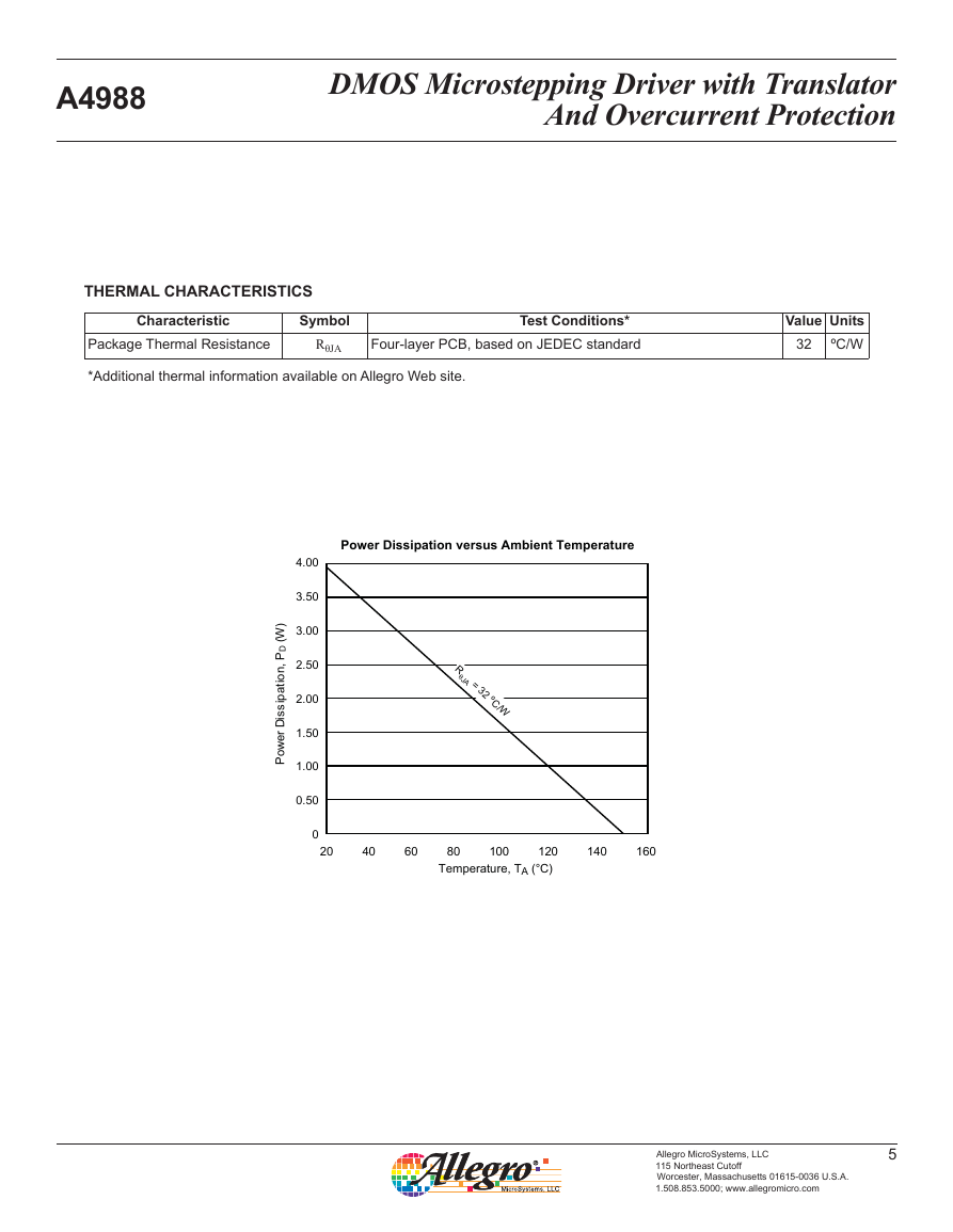
THERMAL CHARACTERISTICS
Characteristic
Package Thermal Resistance
Symbol
RθJA
Four-layer PCB, based on JEDEC standard
Test Conditions*
Value Units
ºC/W
32
*Additional thermal information available on Allegro Web site.
Power Dissipation versus Ambient Temperature
4.00
3.50
3.00
2.50
2.00
1.50
1.00
0.50
)
W
(
D
P
,
n
o
i
t
a
p
i
s
s
D
i
r
e
w
o
P
0
20
R
J
A = 3
2 º
C/
W
40
60
100
80
120
Temperature, TA (°C)
140
160
Allegro MicroSystems, LLC
115 Northeast Cutoff
Worcester, Massachusetts 01615-0036 U.S.A.
1.508.853.5000; www.allegromicro.com
5
�
A4988
DMOS Microstepping Driver with Translator
And Overcurrent Protection
t A
t B
STEP
MS1, MS2, MS3,
RESET, or DIR
t C
t D
Time Duration
Symbol
STEP minimum, HIGH pulse width
STEP minimum, LOW pulse width
Setup time, input change to STEP
Hold time, input change to STEP
tA
tB
tC
tD
Typ.
1
1
200
200
Unit
μs
μs
ns
ns
Figure 1. Logic Interface Timing Diagram
Table 1. Microstepping Resolution Truth Table
MS1 MS2 MS3 Microstep Resolution Excitation Mode
L
H
L
H
H
L
L
H
H
H
L
L
L
L
H
Full Step
Half Step
Quarter Step
Eighth Step
Sixteenth Step
2 Phase
1-2 Phase
W1-2 Phase
2W1-2 Phase
4W1-2 Phase
Allegro MicroSystems, LLC
115 Northeast Cutoff
Worcester, Massachusetts 01615-0036 U.S.A.
1.508.853.5000; www.allegromicro.com
6
�
A4988
DMOS Microstepping Driver with Translator
And Overcurrent Protection
Functional Description
Functional Description
Device Operation. The A4988 is a complete microstepping
motor driver with a built-in translator for easy operation with
minimal control lines. It is designed to operate bipolar stepper
motors in full-, half-, quarter-, eighth, and sixteenth-step modes.
The currents in each of the two output full-bridges and all of the
N-channel DMOS FETs are regulated with fixed off-time PWM
(pulse width modulated) control circuitry. At each step, the current
for each full-bridge is set by the value of its external current-sense
resistor (RS1 and RS2), a reference voltage (VREF), and the output
voltage of its DAC (which in turn is controlled by the output of
the translator).
At power-on or reset, the translator sets the DACs and the phase
current polarity to the initial Home state (shown in figures 8
through 12), and the current regulator to Mixed Decay Mode for
both phases. When a step command signal occurs on the STEP
input, the translator automatically sequences the DACs to the
next level and current polarity. (See table 2 for the current-level
sequence.) The microstep resolution is set by the combined effect
of the MSx inputs, as shown in table 1.
When stepping, if the new output levels of the DACs are lower
than their previous output levels, then the decay mode for the
active full-bridge is set to Mixed. If the new output levels of the
DACs are higher than or equal to their previous levels, then the
decay mode for the active full-bridge is set to Slow. This auto-
matic current decay selection improves microstepping perfor-
mance by reducing the distortion of the current waveform that
results from the back EMF of the motor.
Microstep Select (MSx). The microstep resolution is set by
the voltage on logic inputs MSx, as shown in table 1. The MS1 and
MS3 pins have a 100 kΩ pull-down resistance, and the MS2 pin
has a 50 kΩ pull-down resistance. When changing the step mode
the change does not take effect until the next STEP rising edge.
If the step mode is changed without a translator reset, and abso-
lute position must be maintained, it is important to change the
step mode at a step position that is common to both step modes in
order to avoid missing steps. When the device is powered down,
or reset due to TSD or an over current event the translator is set to
the home position which is by default common to all step modes.
Mixed Decay Operation. The bridge operates in Mixed
decay mode, at power-on and reset, and during normal running
according to the ROSC configuration and the step sequence, as
shown in figures 8 through 12. During Mixed decay, when the trip
point is reached, the A4988 initially goes into a fast decay mode
for 31.25% of the off-time, tOFF . After that, it switches to Slow
decay mode for the remainder of tOFF. A timing diagram for this
feature appears on the next page.
Typically, mixed decay is only necessary when the current in the
winding is going from a higher value to a lower value as determined
by the state of the translator. For most loads automatically-selected
mixed decay is convenient because it minimizes ripple when the
current is rising and prevents missed steps when the current is falling.
For some applications where microstepping at very low speeds is
necessary, the lack of back EMF in the winding causes the current to
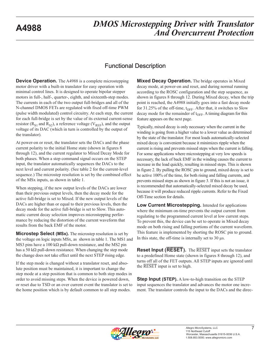
increase in the load quickly, resulting in missed steps. This is shown
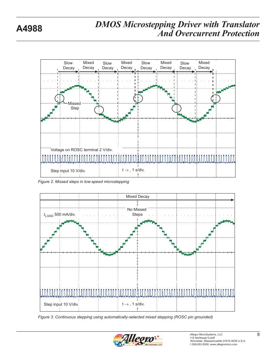
in figure 2. By pulling the ROSC pin to ground, mixed decay is set to
be active 100% of the time, for both rising and falling currents, and
prevents missed steps as shown in figure 3. If this is not an issue, it
is recommended that automatically-selected mixed decay be used,
because it will produce reduced ripple currents. Refer to the Fixed
Off-Time section for details.
Low Current Microstepping. Intended for applications
where the minimum on-time prevents the output current from
regulating to the programmed current level at low current steps.
To prevent this, the device can be set to operate in Mixed decay
mode on both rising and falling portions of the current waveform.
This feature is implemented by shorting the ROSC pin to ground.
In this state, the off-time is internally set to 30 μs.
Reset Input (¯R¯ ¯E¯ ¯S¯ ¯E¯ ¯T¯ ). The ¯R¯ ¯E¯ ¯S¯ ¯E¯ ¯T¯ input sets the translator
to a predefined Home state (shown in figures 8 through 12), and
turns off all of the FET outputs. All STEP inputs are ignored until
the ¯R¯ ¯E¯ ¯S¯ ¯E¯ ¯T¯ input is set to high.
Step Input (STEP). A low-to-high transition on the STEP
input sequences the translator and advances the motor one incre-
ment. The translator controls the input to the DACs and the direc-
Allegro MicroSystems, LLC
115 Northeast Cutoff
Worcester, Massachusetts 01615-0036 U.S.A.
1.508.853.5000; www.allegromicro.com
7
�
A4988
DMOS Microstepping Driver with Translator
And Overcurrent Protection
Slow
Decay
Mixed
Decay
Slow
Decay
Mixed
Decay
Slow
Decay
Mixed
Decay
Slow
Decay
Mixed
Decay
Missed
Step
Voltage on ROSC terminal 2 V/div.
Step input 10 V/div.
t → , 1 s/div.
Figure 2. Missed steps in low-speed microstepping
ILOAD 500 mA/div.
Mixed Decay
No Missed
Steps
Step input 10 V/div.
t → , 1 s/div.
Figure 3. Continuous stepping using automatically-selected mixed stepping (ROSC pin grounded)
Allegro MicroSystems, LLC
115 Northeast Cutoff
Worcester, Massachusetts 01615-0036 U.S.A.
1.508.853.5000; www.allegromicro.com
8
�




 2023年江西萍乡中考道德与法治真题及答案.doc
 2012年重庆南川中考生物真题及答案.doc
 2013年江西师范大学地理学综合及文艺理论基础考研真题.doc
 2020年四川甘孜小升初语文真题及答案I卷.doc
 2020年注册岩土工程师专业基础考试真题及答案.doc
 2023-2024学年福建省厦门市九年级上学期数学月考试题及答案.doc
 2021-2022学年辽宁省沈阳市大东区九年级上学期语文期末试题及答案.doc
 2022-2023学年北京东城区初三第一学期物理期末试卷及答案.doc
 2018上半年江西教师资格初中地理学科知识与教学能力真题及答案.doc
 2012年河北国家公务员申论考试真题及答案-省级.doc
 2020-2021学年江苏省扬州市江都区邵樊片九年级上学期数学第一次质量检测试题及答案.doc
 2022下半年黑龙江教师资格证中学综合素质真题及答案.doc