AN1211
Maximum Power Solar Converter
Author:
John Charais
Microchip Technology Inc.
the development of
INTRODUCTION
As the need for remote operation of electronic devices
continues to increase, power for these devices becomes
more of a concern. Remote applications are powered
mostly by batteries that are either recharged or changed
on a regular basis. The more remote the location is, the
bigger the challenge becomes of replacing these
batteries. Since
the modern
photovoltaic cell in 1954, remotely powered applications
that do not have to be serviced became possible.
The focus of this application note is to identify how to
get the maximum power out of a solar panel to power a
remote application. The Maximum Power Point
Converter is essentially a DC-to-DC converter, where
the DC input voltage is a solar panel and the output
voltage is 28 volts. The intent of the converter is to
show how to take the solar panel and generate a
voltage capable of recharging a 24-volt battery.
Although the chemistry of the battery and how to
charge the battery properly are extremely important to
the actual design, these details will not be covered in
this application note. Also associated with
this
application note is a zip file with source code and Excel
spreadsheet.
SOLAR PANELS
Solar Panels are an array of solar cells. The
characteristics of the solar panel are essentially the
same as those of the solar cells, only scaled up in
voltage or current based on the number of solar cells
used and the arrangement of the array. Solar panels
come in a variety of shapes, sizes and efficiencies, but
all have similar characteristics.
A solar panel will generate its maximum voltage when
the panel is in full sunlight with no load. This voltage is
commonly referred to as the open circuit voltage (VOC)
of the panel. As the load of the solar panel increases,
the output voltage of the solar panel will decrease in a
nonlinear fashion until the maximum output current, the
short circuit current (JSC) of the panel, is reached.
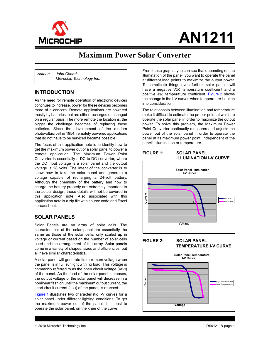
Figure 1 illustrates two characteristic I-V curves for a
solar panel under different lighting conditions. To get
the maximum power out of the panel, it is best to
operate the solar panel, on the knee of the curve.
From these graphs, you can see that depending on the
illumination of the panel, you want to operate the panel
at different load points to maximize the output power.
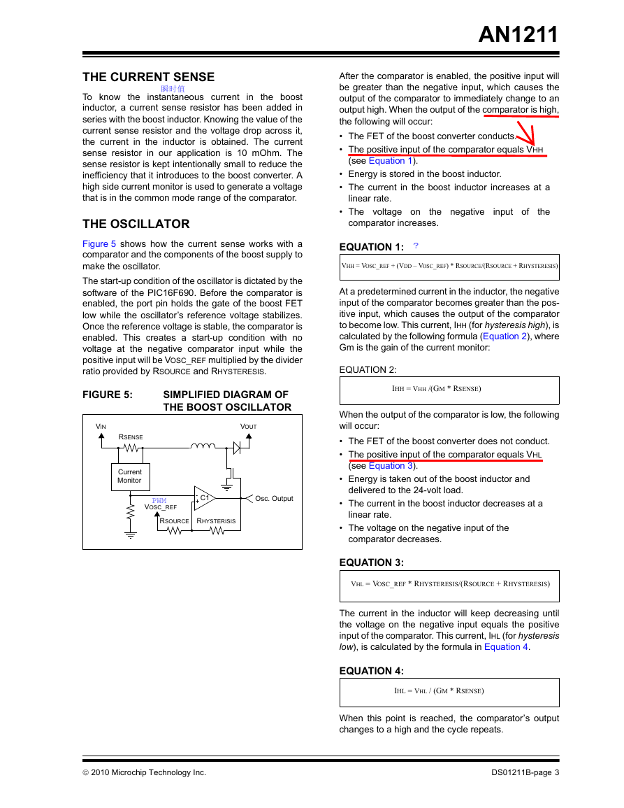
To complicate things even further, solar panels will
have a negative VOC temperature coefficient and a
positive JSC temperature coefficient. Figure 2 shows
the change in the I-V curves when temperature is taken
into consideration.
The relationship between illumination and temperature
make it difficult to estimate the proper point at which to
operate the solar panel in order to maximize the output
power. To solve this problem, the Maximum Power
Point Converter continually measures and adjusts the
power out of the solar panel in order to operate the
panel at its maximum power point, independent of the
panel’s illumination or temperature.
FIGURE 1:
SOLAR PANEL
ILLUMINATION I-V CURVE
Solar Panel Illumination
Voltage
t
n
e
r
r
u
C
Full Sun
0.51
0.5
0.5
0.497
0.495
0.492
0.487
0.47
0.35
0.3
0
0
5
10
20
25
30
35
40
45
47
50
I-V Curve
Partial Sun High Tem Low Temp
0.47685
0.4675
0.4675
0.5467 0.464695
0.5445 0.462825
0.4505
0.45
0.44
0.38
0.28
0
0.4335
0.425
0.425
0.42245
0.42075
0.4182
0.41
0.35
0.025
0
0
0.561
0.55
0.55
0.53
0.4
0.035
0
0
0
Full Sun
Partial Sun
Voltage
FIGURE 2:
SOLAR PANEL
TEMPERATURE I-V CURVE
Solar Panel Temperature
I-V Curve
t
n
e
r
r
u
C
High Temperatures
Low Temperatures
Voltage
2010 Microchip Technology Inc.
DS01211B-page 1
�
AN1211
OVERVIEW
For this project we will be using a 10-volt open circuit
solar panel with a short circuit current of 2.5 amps. With
an open circuit voltage of 10 volts, a boost converter is
needed to charge the 24-volt battery. See Figure 3.
FIGURE 3:
BOOST CONVERTER
Solar
Panel
Battery
To get the solar panel to operate at its maximum power
point, there are a few items needed. First, in order to
know the output power of the solar panel, both the
current and voltage of the solar panel have to be
monitored. This will be accomplished by a high side
current monitor and simple resistor divider on the solar
panel’s output voltage. There also needs to be a way to
control the output power of the solar panel. This is done
by manipulating the panel’s output current. And lastly,
a software algorithm is needed to know which way to
manipulate the current (e.g., whether the current out of
the solar panel should be increased or decreased).
To make the Maximum Power Point Converter work,
the functions of the boost converter need to be merged
with the solar panel’s output load. The boost converter
is either storing current in the boost inductor (switch
closed) or it is delivering current from the boost inductor
to the load (switch opened). When the boost inductor is
storing current, the current comes from the solar panel.
In essence, the boost inductor is the solar panel’s load.
By making the current stored in the boost inductor
programmable, the load of the solar panel becomes
programmable. This is the principal on how the
Maximum Power Point Converter works. The Maximum
Power Point Converter combines a boost converter, a
programmable current oscillator and a software
algorithm to maximize the power out of a solar panel.
HARDWARE OVERVIEW
Figure 4 shows the block diagram of the Maximum
Power Point Converter.
FIGURE 4:
MAXIMUM POWER POINT CONVERTER
Solar Panel
Current Sense
Boost Supply
Output
Voltage Sense
Oscillator
Max Power
Algorithm
Programmable
Voltage Reference
Over-Voltage
Protection
PIC16F690
DS01211B-page 2
2010 Microchip Technology Inc.
�
THE CURRENT SENSE
To know the instantaneous current in the boost
inductor, a current sense resistor has been added in
series with the boost inductor. Knowing the value of the
current sense resistor and the voltage drop across it,
the current in the inductor is obtained. The current
sense resistor in our application is 10 mOhm. The
sense resistor is kept intentionally small to reduce the
inefficiency that it introduces to the boost converter. A
high side current monitor is used to generate a voltage
that is in the common mode range of the comparator.
THE OSCILLATOR
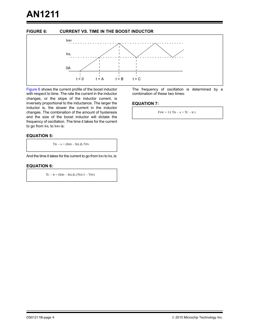
Figure 5 shows how the current sense works with a
comparator and the components of the boost supply to
make the oscillator.
The start-up condition of the oscillator is dictated by the
software of the PIC16F690. Before the comparator is
enabled, the port pin holds the gate of the boost FET
low while the oscillator’s reference voltage stabilizes.
Once the reference voltage is stable, the comparator is
enabled. This creates a start-up condition with no
voltage at the negative comparator input while the
positive input will be VOSC_REF multiplied by the divider
ratio provided by RSOURCE and RHYSTERESIS.
FIGURE 5:
SIMPLIFIED DIAGRAM OF
THE BOOST OSCILLATOR
VOUT
VIN
RSENSE
Current
Monitor
C1-
+
VOSC_REF
RSOURCE
RHYSTERISIS
Osc. Output
AN1211
After the comparator is enabled, the positive input will
be greater than the negative input, which causes the
output of the comparator to immediately change to an
output high. When the output of the comparator is high,
the following will occur:
• The FET of the boost converter conducts.
• The positive input of the comparator equals VHH
(see Equation 1).
• Energy is stored in the boost inductor.
• The current in the boost inductor increases at a
linear rate.
• The voltage on
comparator increases.
the negative
input of
the
EQUATION 1:
VHH = VOSC_REF + (VDD – VOSC_REF) * RSOURCE/(RSOURCE + RHYSTERESIS)
At a predetermined current in the inductor, the negative
input of the comparator becomes greater than the pos-
itive input, which causes the output of the comparator
to become low. This current, IHH (for hysteresis high), is
calculated by the following formula (Equation 2), where
Gm is the gain of the current monitor:
EQUATION 2:
IHH = VHH /(GM * RSENSE)
When the output of the comparator is low, the following
will occur:
• The FET of the boost converter does not conduct.
• The positive input of the comparator equals VHL
(see Equation 3).
• Energy is taken out of the boost inductor and
delivered to the 24-volt load.
• The current in the boost inductor decreases at a
linear rate.
• The voltage on the negative input of the
comparator decreases.
EQUATION 3:
VHL = VOSC_REF * RHYSTERESIS/(RSOURCE + RHYSTERESIS)
The current in the inductor will keep decreasing until
the voltage on the negative input equals the positive
input of the comparator. This current, IHL (for hysteresis
low), is calculated by the formula in Equation 4.
EQUATION 4:
IHL = VHL / (GM * RSENSE)
When this point is reached, the comparator’s output
changes to a high and the cycle repeats.
2010 Microchip Technology Inc.
DS01211B-page 3
�
AN1211
FIGURE 6:
CURRENT VS. TIME IN THE BOOST INDUCTOR
IHH
IHL
0A
t = 0
t = A
t = B
t = C
The frequency of oscillation is determined by a
combination of these two times:
EQUATION 7:
FSW = 1/( TB – A + TC – B )
Figure 6 shows the current profile of the boost inductor
with respect to time. The rate the current in the inductor
changes, or the slope of the inductor current, is
inversely proportional to the inductance. The larger the
inductor is, the slower the current in the inductor
changes. The combination of the amount of hysteresis
and the size of the boost inductor will dictate the
frequency of oscillation. The time it takes for the current
to go from IHL to IHH is:
EQUATION 5:
TB – A = (IHH – IHL)L/VIN
And the time it takes for the current to go from IHH to IHL is:
EQUATION 6:
TC – B = (IHH – IHL)L/(VOUT – VIN)
DS01211B-page 4
2010 Microchip Technology Inc.
�
this
the solar panel. By making
PROGRAMMABLE VOLTAGE
REFERENCE
The voltage reference for the PIC16F690’s first
comparator, C1, will be used to set the RMS current out
of
reference
programmable, it is possible to increase or decrease
the current out of the solar panel independent of the
solar panel’s voltage. The power out of the solar panel
will be controlled by monitoring the voltage and
adjusting the current out of the solar panel’s RMS
current. To implement the programmable voltage
reference, a RC
the
PIC16F690’s PWM, will be used.
Ideally, the current out of the solar panel would be
scalable from 0 amps to approximately 2.75 amps to
slightly exceed the panel’s full range of 0-2.5 amps, but
the hardware setup of the oscillator does not allow for
this to happen. Looking back to our equations for IHH
(Equation 2) and IHL (Equation 4), it can be seen that if
the programmable voltage reference is set to zero, IHL
will be zero, but IHH is determined by the high output of
C1 and the resistor divider set up by RSENSE and
RHYSTERESIS. This creates an inherent DC offset
current equal to half the ripple current in the boost
inductor.
filter,
in combination with
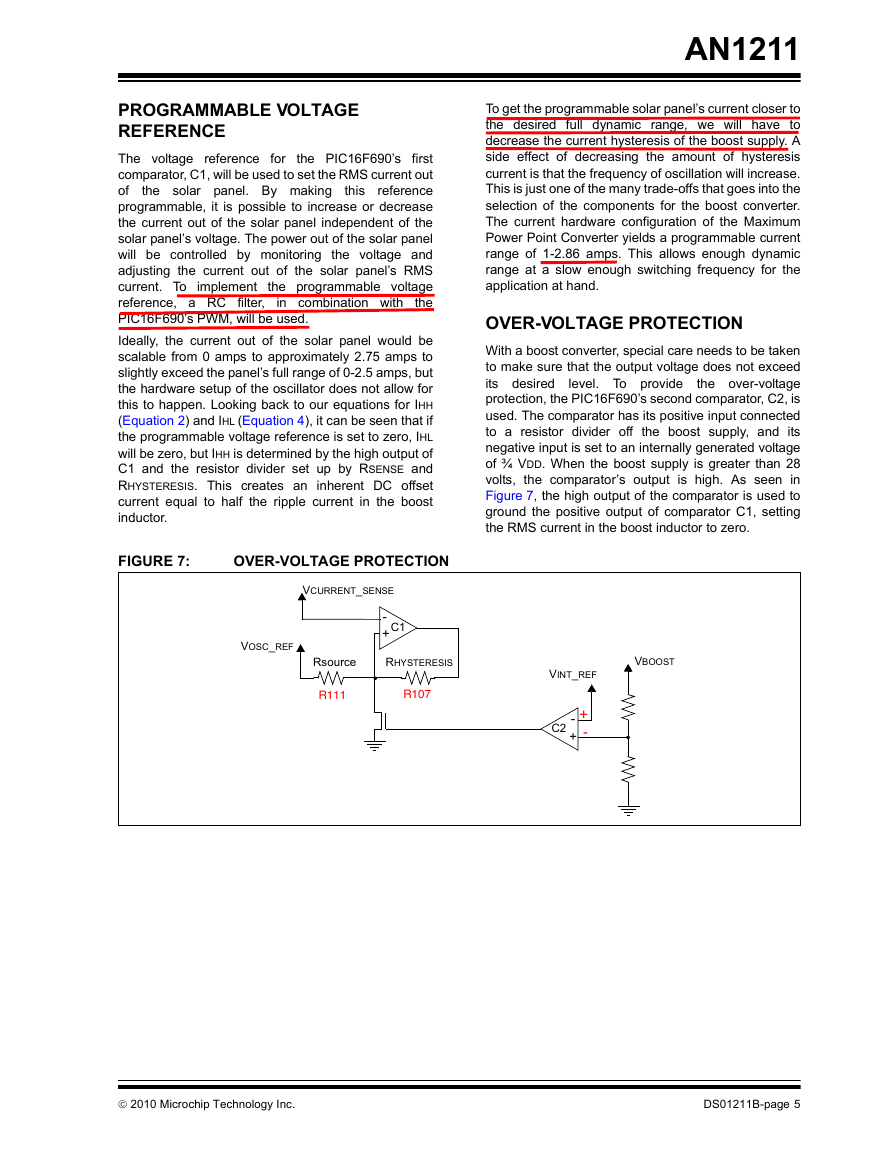
FIGURE 7:
OVER-VOLTAGE PROTECTION
VCURRENT_SENSE
-
+
C1
Rsource
RHYSTERESIS
VOSC_REF
AN1211
To get the programmable solar panel’s current closer to
the desired full dynamic range, we will have to
decrease the current hysteresis of the boost supply. A
side effect of decreasing the amount of hysteresis
current is that the frequency of oscillation will increase.
This is just one of the many trade-offs that goes into the
selection of the components for the boost converter.
The current hardware configuration of the Maximum
Power Point Converter yields a programmable current
range of 1-2.86 amps. This allows enough dynamic
range at a slow enough switching frequency for the
application at hand.
level. To provide
OVER-VOLTAGE PROTECTION
With a boost converter, special care needs to be taken
to make sure that the output voltage does not exceed
its desired
the over-voltage
protection, the PIC16F690’s second comparator, C2, is
used. The comparator has its positive input connected
to a resistor divider off the boost supply, and its
negative input is set to an internally generated voltage
of ¾ VDD. When the boost supply is greater than 28
volts, the comparator’s output is high. As seen in
Figure 7, the high output of the comparator is used to
ground the positive output of comparator C1, setting
the RMS current in the boost inductor to zero.
VBOOST
VINT_REF
-
C2 +
2010 Microchip Technology Inc.
DS01211B-page 5
�
AN1211
COMPONENT SELECTION
Keeping in mind that the goal of this project is to get the
most power out of the solar panel, it would seem
unwise to waste power by having an inefficient boost
power supply. In order to optimize the efficiency of the
boost supply, we first need to examine the losses
associated with each component. Below are a series of
power equations associated with each major
component of the boost supply. For further analysis of
the interaction of these equations, download the Excel
spreadsheet associated with this application note.
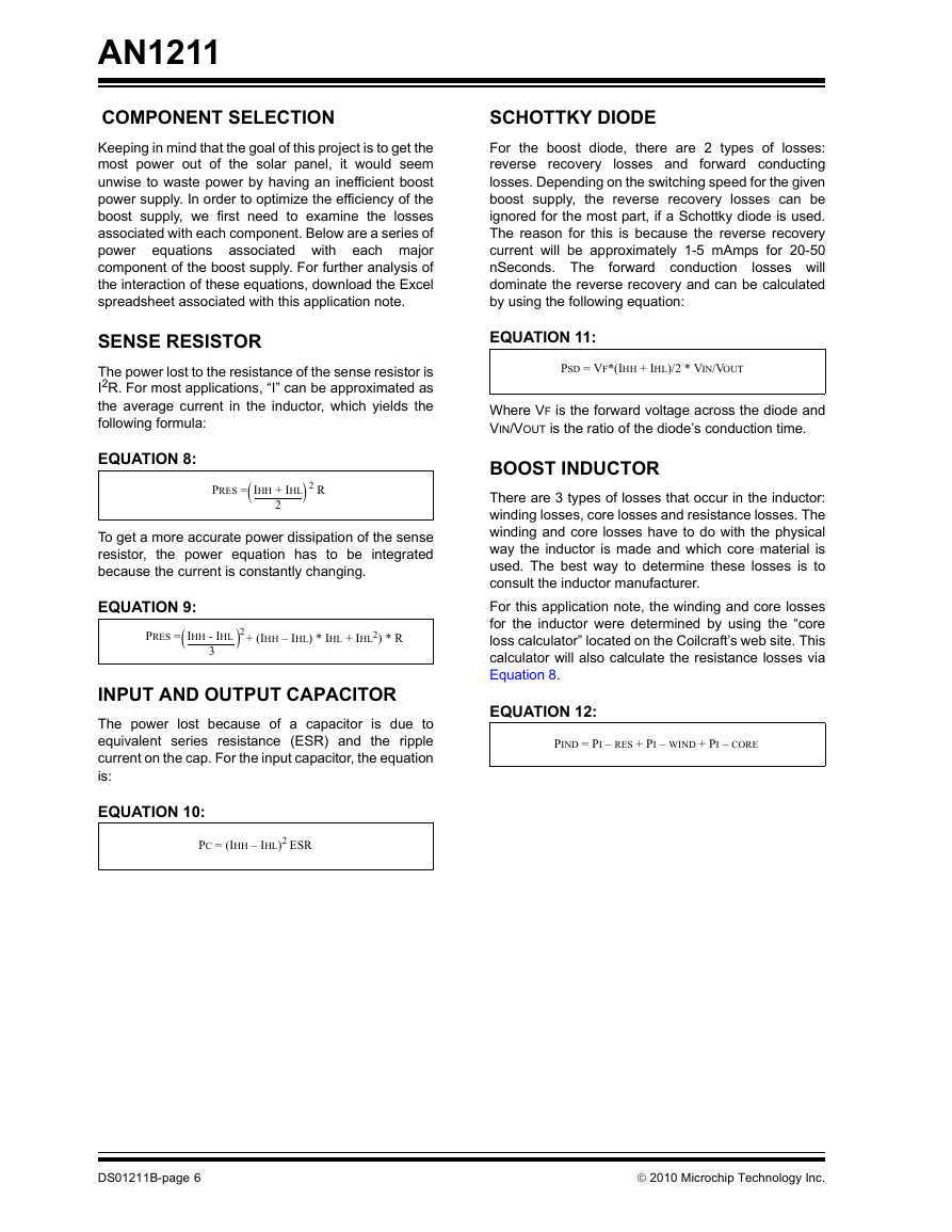
SENSE RESISTOR
The power lost to the resistance of the sense resistor is
I2R. For most applications, “I” can be approximated as
the average current in the inductor, which yields the
following formula:
EQUATION 8:
PRES = IHH + IHL 2 R
(
)
2
To get a more accurate power dissipation of the sense
resistor, the power equation has to be integrated
because the current is constantly changing.
EQUATION 9:
(
3
PRES = IHH - IHL 2
) + (IHH – IHL) * IHL + IHL2) * R
INPUT AND OUTPUT CAPACITOR
The power lost because of a capacitor is due to
equivalent series resistance (ESR) and the ripple
current on the cap. For the input capacitor, the equation
is:
EQUATION 10:
PC = (IHH – IHL)2 ESR
SCHOTTKY DIODE
For the boost diode, there are 2 types of losses:
reverse recovery losses and
forward conducting
losses. Depending on the switching speed for the given
boost supply, the reverse recovery losses can be
ignored for the most part, if a Schottky diode is used.
The reason for this is because the reverse recovery
current will be approximately 1-5 mAmps for 20-50
nSeconds. The
losses will
dominate the reverse recovery and can be calculated
by using the following equation:
forward conduction
EQUATION 11:
PSD = VF*(IHH + IHL)/2 * VIN/VOUT
Where VF is the forward voltage across the diode and
VIN/VOUT is the ratio of the diode’s conduction time.
BOOST INDUCTOR
There are 3 types of losses that occur in the inductor:
winding losses, core losses and resistance losses. The
winding and core losses have to do with the physical
way the inductor is made and which core material is
used. The best way to determine these losses is to
consult the inductor manufacturer.
For this application note, the winding and core losses
for the inductor were determined by using the “core
loss calculator” located on the Coilcraft’s web site. This
calculator will also calculate the resistance losses via
Equation 8.
EQUATION 12:
PIND = PI – RES + PI – WIND + PI – CORE
DS01211B-page 6
2010 Microchip Technology Inc.
�
AN1211
With the components on the current bill of material, the
calculated efficiency of the boost supply is 96.56%,
when the input voltage is 8 volts and the input current
is 2.5 amps. Testing on the Maximum Power Point
Converter has shown that the overall process converts
efficiency to 94%. This is slightly less than what is
calculated, because we only account for the efficiency
of the boost supply, and did not account for the
quiescent current draw of the FET driver, PIC16F690,
current monitor, etc.
BOOST FET
The losses due to the boost FET can be broken up into
two categories: conduction losses and switching
losses. For the conduction loss, it is the resistance loss
of the FET multiplied by the ratio of the FET’s on/off
time.
EQUATION 13:
(
)
PRDS = IHH + IHL 2
2
* RDS*(1 – VIN/VOUT)
Or, for the more accurate loss:
EQUATION 14:
PRDS = (IHH – IHL)2
(
3
+(IHH – IHL) IHL + IHL2) *RDS*(1 – VIN/VOUT)
The switching losses can be broken up into 3 different
categories: gate charge, output capacitance, and
transition losses calculated by the following equations:
EQUATION 15:
PGATE = Fsw*QG*VDRIVE
EQUATION 16:
PCOSS = (COSS*VDS2*FSW)/2
EQUATION 17:
PTRAN = ½(TR + TF)VOUT*IIN*FSW
EQUATION 18:
PFET = PGATE + PCOSS + PTRAN
FSW is the switching frequency of the boost supply, QG
is the FET’s total gate charge, VDRIVE is the voltage the
gate is being driven to, and TR/TF is the FET’s turn
on/off rise/fall time.
The total power lost due to the switching power supply
is:
EQUATION 19:
PTOTAL = PRES + PCIN + PCOUT + PSD + PI-RES + PIND + PIFET
2010 Microchip Technology Inc.
DS01211B-page 7
�
AN1211
SOFTWARE
The software to control the Maximum Power Point
Converter can be broken into two algorithms: Current
Reduction and the dither routine, which are controlled
via the Interrupt Service Routine (ISR). Both algorithms
manipulate the current of the solar panel via the
Programmable Voltage reference generated by the
PIC16F690’s 10-bit PWM.
By modifying the duty cycle of the PWM, the current out
of the solar panel will scale linearly with respect to the
duty cycle of PWM. To simplify the math for both
algorithms, only the 8 MSBs of the PWM’s duty cycle
will be used, yielding 256 discrete current settings for
the solar panel.
DITHER ROUTINE
The dither routine is used to optimize the power out of
the solar panel. The algorithm does not use the exact
power out of the solar panel, but rather, a difference in
the proportional power. For the dither routine, only the
relative difference between two successive power
calculations is important. Did the power increase or did
the power decrease? The amount the power changed
has no effect on the algorithm. For this reason, the
exact power out of the solar panel is not required,
which allows us to use the linear relationship of the
PWM’s duty cycle and the solar panels current. The
proportional power out of the solar panel is calculated
by multiplying the voltage of the solar panel by the duty
cycle of the PWM. For simplicity, the 8 Most Significant
Bytes (MSBs) of PWM’s duty cycle is multiplied by the
8 MSBs of the A/D reading on the solar panels voltage.
FIGURE 8:
DITHER ROUTINE
)
s
p
m
A
(
t
n
e
r
r
u
C
0
3
5
10
20
2.5
25
30
2
35
40
45
1.5
50
1
0.5
0
0
Solar Panel I-V Curve
50 Cells in a 5x10 array
0
1
2
4
5
6
7
8
9
10
0.51
0.5
0.5
0.497
0.495
0.492
0.487
0.47
0.35
0
2.55
2.5
2.5
2.485
2.475
2.46
2.435
2.35
1.75
0
0.25
0.25
0.25
0.245
0.244
0.24
0.238
0.2
0.08
0
0
2.5
5
9.94
12.375
14.76
17.045
18.8
15.75
0
0
2.5
5
9.94
12.375
14.76
17.045
18.8
15.75
0
0
1.25
2.5
4.9
6.1
7.2
8.33
8
3.6
0
Full Sun
2
4
6
8
10
12
Voltage (Volts)
Using the PWM duty cycle for the solar panel’s current
has two benefits. The first benefit is that it eliminates
the need for additional hardware. To get the exact
current out of the solar panel, an analog buffer on ROUT
is needed, as well as an additional RC filter located on
the buffer’s output. The second benefit is that the
PWM’s duty cycle is already in a digital format
speeding up the control loop, because there is no need
to perform a second A/D conversion.
Figure 8 shows the I-V curve and the maximum power
curve of the solar panel the Maximum Power Point
Converter was designed for. Starting with no load on
the output, we have an open-circuit voltage of 10 volts.
When the panel is operating at this voltage, the panel
produces no power. By increasing the current taken out
of the panel, we begin to collapse the solar panels
voltage, but gain power. If the current out of the panel
is increased beyond a certain point, the supply voltage
will quickly collapse and the power out of the solar
panel will decrease.
The
the
proportional power of the solar panel is calculated by
multiplying the voltage of the solar panel by the
minimum duty cycle of the PWM. After the power has
been calculated, the PWM’s duty cycle is increased
and the direction flag is set to indicate that the current
out of the panel was increased (if the current out of the
panel was decreased, the direction flag would be
cleared). The second time through the dither routine,
the power is again calculated and compared to the
previous power calculation. If the power increases, the
current will be adjusted in the same manner as
indicated by the direction flag; in this case, the current
would be increased. This will continue to happen until
the power decreases. When the power decreases, the
current is adjusted in the opposite manner as indicated
by the direction flag (decreased), and then the direction
flag is cleared.
the dither
routine,
first
time
through
Solar Panel Power Curve
50 cells in a 5x10 array
Full Sun
0
2
4
6
8
Voltage (Volts)
10
12
)
s
t
t
a
W
(
r
e
w
o
P
20
15
10
5
0
DS01211B-page 8
2010 Microchip Technology Inc.
�




 2023年江西萍乡中考道德与法治真题及答案.doc
 2012年重庆南川中考生物真题及答案.doc
 2013年江西师范大学地理学综合及文艺理论基础考研真题.doc
 2020年四川甘孜小升初语文真题及答案I卷.doc
 2020年注册岩土工程师专业基础考试真题及答案.doc
 2023-2024学年福建省厦门市九年级上学期数学月考试题及答案.doc
 2021-2022学年辽宁省沈阳市大东区九年级上学期语文期末试题及答案.doc
 2022-2023学年北京东城区初三第一学期物理期末试卷及答案.doc
 2018上半年江西教师资格初中地理学科知识与教学能力真题及答案.doc
 2012年河北国家公务员申论考试真题及答案-省级.doc
 2020-2021学年江苏省扬州市江都区邵樊片九年级上学期数学第一次质量检测试题及答案.doc
 2022下半年黑龙江教师资格证中学综合素质真题及答案.doc