High efficiency、Ultralow distortion、Constant large volume、Sixth
generation Class K Audio Amplifier
AW8736 Data Sheet
May 2013 V1.5
FEATURES
New generation charge pump technology :
K-Chargepump,efficiency reaches as high as
92%
Power amplifier overall efficiency 75%,greatly
prolong mobile phone usage time
Ultra-low distortion:0.02%
Within Lithium battery voltage range, output
power is maintained constant
Output Power level:0.8W、1W、1.2W
Second generation Non-crack-noise
(NCN)
technology
Super TDD-Noise suppression
Ultra-low EMI
One wire pulse control
High PSRR:-65dB(217Hz)
Small 2mm×2mm FC-16package
APPLICATIONS
Smart phone
DEVICE PINOUT
DESCRIPTION
AW8736 is designed to enhance smart mobile phone
sound quality,which is a new high efficiency, ultra-low
distortion, constant large volume, sixth generation class
K audio amplifiers. Using a new generation of charge
pump technology:K -Chargepump structure, efficiency
as high as 92%, power amplifier’s overall efficiency
reaches 75%, greatly prolong the mobile phone usage
time.
unique
non-crack-noise (NCN) technology brings high quality
music enjoyment.
distortion
ultra-low
0.02%
and
AW8736 integrated K-Chargepump booster circuit,
the output power cannot drop along with lithium battery
voltage lower down. Within lithium battery voltage
range(3.3 V - 4.35V), output power is constant, providing
high quality music enjoyment. AW8736 has 0.8 W, 1 W
and 1.2 W three output power level, recommended using
rated power of 0.7W and above speakers, which
greatly improve the volume, and effectively protect
speakers.
The AW8736 uses awinic proprietary TDD-Noise
suppression
suppression
technology, effectively restrain TDD-Noise and EMI
interference.
and EMI
technology
over
built-in
AW8736
protection,
over-temperature protection and short circuit protection
function, effectively protect the chip. The AW8736 uses
small 2mmx2mm FC-16 package.
current
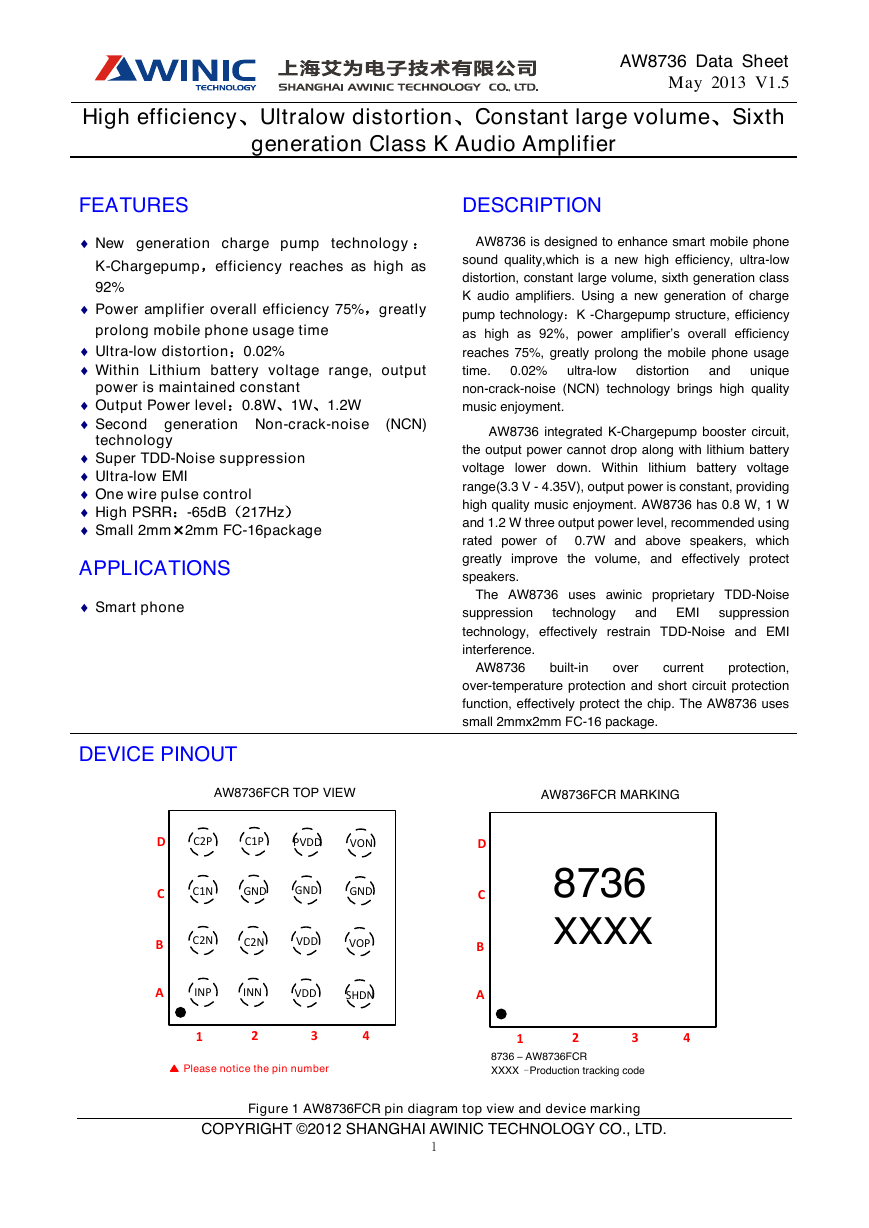
Figure 1 AW8736FCR pin diagram top view and device marking
COPYRIGHT ©2012 SHANGHAI AWINIC TECHNOLOGY CO., LTD.
1
AW8736FCR TOP VIEWINPINNSHDNGNDPVDDC2NC2NC2PC1PC1NVDDVDDVOPVONGND1234ABCDGND1234ABCD8736XXXXAW8736FCR MARKING8736 – AW8736FCRXXXX–Production tracking codePlease notice the pin number�
High efficiency、Ultralow distortion、Constant large volume、Sixth
generation Class K Audio Amplifier
PIN DESCRIPTION
AW8736 Data Sheet
May 2013 V1.5
Number
Symbol
Description
A1
A2
A3,B3
A4
B1
B2
B4
C1
C2
C3
C4
D1
D2
D3
D4
INP
INN
VDD
SHDN
C2N
VOP
C1N
GND
C2P
C1P
PVDD
VON
Positive audio input terminal
Negative audio input terminal
Power supply
Chip power down pin,active low;one wire pulse control;
Negative side of the external charge pump flying capacitor C2
Positive audio output terminal
Negative side of the external charge pump flying capacitor C1
Ground
Positive side of the external charge pump flying capacitor C2
Positive side of the external charge pump flying capacitor C1
Boost charge pump output voltage
Negative audio output terminal
APPLICATION DIAGRAM
Figure 2 AW8736 single-ended input application diagram (Note 1)
Note1:when single-ended input,input audio signal can arbitrarily connect to one of INN,INP input terminal,
the other terminal connects to ground through input capacitor and resistance.
COPYRIGHT ©2012 SHANGHAI AWINIC TECHNOLOGY CO., LTD.
2
C1PAW8736C1NCOUT4.7uFPVDDINPINN3KΩ15nF3KΩ15nFCinCinRinRinVOPVONGNDVDDSHDNPulse Input12CF12.2uFCS14.7uFVBAT34C1220pFA4A2A1C2,C3,C4B4D4B1B2C21nFC31nFD3A3,B3D2C1C2PC2NCF22.2uFB1,B2D1CS20.1uFSingle-Ended Input�
AW8736 Data Sheet
May 2013 V1.5
High efficiency、Ultralow distortion、Constant large volume、Sixth
generation Class K Audio Amplifier
Filter capacitor Cs suggest using X7R/X5R ceramic capacitors, if using tantalum capacitors, one ceramic
capacitor greater than 1 uF must be placed near the VDD pin to filter high frequency interference signal.
Figure 3 AW8736 differential input application diagram
ORDERING INFORMATION
Product Type
Operation temperature range
Package
Device Marking
Delivery Form
AW8736FCR
-40℃~85℃
FC-16
8736
Tape and Reel
3000 pcs
COPYRIGHT ©2012 SHANGHAI AWINIC TECHNOLOGY CO., LTD.
3
C1PAW8736C1NCOUT4.7uFPVDDINPINN3KΩ15nF3KΩ15nFCinCinRinRinVOPVONGNDVDDSHDNPulse Input12CF12.2uFCS14.7uFVBAT34C1220pFA4A2A1C2,C3,C4B4D4B1B2C21nFC31nFD3A3,B3D2C1C2PC2NCF22.2uFB1,B2D1CS20.1uFDifferential InputAW8736ShipmentR: Tape & ReelPackage typeFC: FC16�
High efficiency、Ultralow distortion、Constant large volume、Sixth
generation Class K Audio Amplifier
ABSOLUTE MAXIMUM RATING(Note2)
AW8736 Data Sheet
May 2013 V1.5
Parameter
Supply Voltage VDD
Range
-0.3V to 6V
INP,INN Input Pin Voltage
-0.3V to VDD+0.3V
Package Thermal Resistance θJA
69℃/W
Ambient Temperature Range
-40℃ to 85℃
Maximum Junction Temperature TJMAX
125℃
Storage Temperature Range TSTG
-65℃ to 150℃
Lead Temperature(Soldering 10 Seconds)
ESD Rating(Note 3)
HBM(human body model)
Latch-up
Test Condition:JEDEC STANDARD NO.78B DECEMBER 2008
260℃
±6KV
+IT:450mA
-IT:-450mA
Note 2:Stresses beyond those listed under "absolute maximum ratings" may cause permanent damageto the device.
These are stress ratings only and functional operation of the device at these or any other conditions beyond those
indicated under "recommended operating conditions" is not implied. Exposure to absolute-maximum-rated conditions
for extended periods may affect device reliability.
Note 3:The human body model is a 100pF capacitor discharged through a 1.5kΩ resistor into each pin. Test method:
MIL-STD-883G Method 3015.7
MODE DESCRIPTION
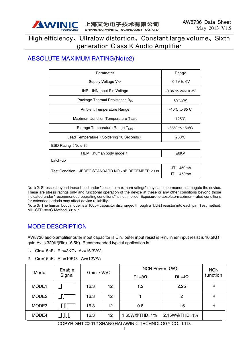
AW8736 audio amplifier outer input capacitor is Cin,outer input resist is Rin,inner input resist is 16.5KΩ,
gain Av is 320K/(Rin+16.5K). Recommended typical application is:
1、 Cin=15nF,Rin=3KΩ,Av=16.3V/V;
2、 Cin=15nF,Rin=10KΩ,Av=12V/V;
Mode
MODE1
MODE2
MODE3
MODE4
Enable
Signal
Gain(V/V)
NCN Power(W)
RL=8Ω
RL=4Ω
NCN
function
16.3
16.3
16.3
16.3
12
12
12
12
1.2
1
0.8
2.25
2
1.6
1.65W@THD=1%
2.15W@THD=1%
√
√
√
COPYRIGHT ©2012 SHANGHAI AWINIC TECHNOLOGY CO., LTD.
4
�
High efficiency、Ultralow distortion、Constant large volume、Sixth
generation Class K Audio Amplifier
AW8736 Data Sheet
May 2013 V1.5
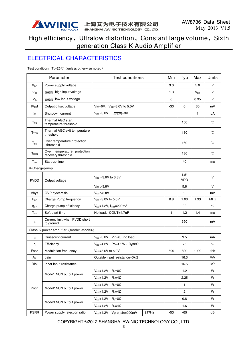
ELECTRICAL CHARACTERISTICS
Test condition:TA=25℃(unless otherwise noted)
Parameter
Test conditions
Min Typ Max Units
VDD
Power supply voltage
VIH
VIL
high input voltage
low input voltage
|VOS|
Output offset voltage
Vin=0V,VDD=3.0V to 5.0V
ISD
Shutdown current
VDD=3.6V,
=0V
TTG
TTGR
TSD
TSDR
Thermal AGC start
temperature threshold
Thermal AGC exit temperature
threshold
Over temperature protection
threshold
Over temperature protection
recovery threshold
TON
Start-up time
K-Chargepump
PVDD Output voltage
Vhys
OVP hysteresis
VDD =3.0V to 3.8V
VDD >3.8V
VDD >3.8V
3.0
1.3
0
-30
0
150
130
160
130
40
1.5*
VDD
5.8
50
5.0
VDD
0.35
30
1
V
V
V
mV
μA
℃
℃
℃
℃
ms
V
V
mV
Charge Pump frequency
VDD=3.0V to 5.0V
0.8
1.06
1.33
MHz
FCP
ηCP
TST
IL
Charge pump efficiency
VDD=4.2V, Iload=200mA
Soft-start time
No load,COUT=4.7uF
Current limit when PVDD short
to ground
Class K power amplifier(mode1-mode4)
Iq
η
Quiescent current
VDD=3.6V,Vin=0,no load
Efficiency
VDD=4.2V,Po=1.2W,RL=8Ω
1
92
1.2
350
9.5
75
1.4
%
ms
mA
mA
%
Fosc
Modulation frequency
VDD=3.0V to 5.0V
600
800
1000
kHz
Av
gain
Outside input resistance=3kΩ
Rini
Inner input resistance
Mode1 NCN output power
Pncn
Mode2 NCN output power
Mode3 NCN output power
VDD=4.2V,RL=8Ω
VDD=4.2V,RL=4Ω
VDD=4.2V,RL=8Ω
VDD=4.2V,RL=4Ω
VDD=4.2V,RL=8Ω
VDD=4.2V,RL=4Ω
16.3
16.5
1.2
2.25
1
2
0.8
1.6
PSRR
Power supply rejection ratio
VDD=4.2V,Vp-p_sin=200mV
217Hz
-53
-65
COPYRIGHT ©2012 SHANGHAI AWINIC TECHNOLOGY CO., LTD.
5
V/V
kΩ
W
W
W
W
W
W
dB
SHDNSHDNSHDN�
High efficiency、Ultralow distortion、Constant large volume、Sixth
generation Class K Audio Amplifier
AW8736 Data Sheet
May 2013 V1.5
1kHz
-53
-65
0.75
0.75
150
150
84.5
87.5
155
0.02
0.02
2.0
1.65
1.5
1.23
2.58
2.15
1.85
1.55
2
2
10
10
500
500
dB
dB
dB
uVrms
%
%
W
W
W
W
W
W
W
W
us
us
us
us
ms
s
dB
SNR
Signal-to-noise ratio
VDD=4.2V,Po=0.8W,RL=8Ω
VDD=4.2V,Po=1.65W,RL=8Ω
Vn
Output noise voltage
VDD=4.2V,f=20Hz to 20kHz,
input ac grounded
A-weighting
THD+N
Total harmonic
distortion+noise
PO
Mode4 output power
VDD=4.2V,Po=1W,RL=8Ω,f=1kHz,Mode1
VDD=4.2V,Po=1.2W,RL=8Ω,f=1kHz,Mode4
THD+N=10%,f=1kHz,RL=8Ω,VDD=4.2V
THD+N=1%,f=1kHz,RL=8Ω,VDD=4.2V
THD+N=10%,f=1kHz,RL=8Ω,VDD=3.6V
THD+N=1%,f=1kHz,RL=8Ω,VDD=3.6V
THD+N=10%,f=1kHz,RL=4Ω,VDD=4.2V
THD+N=1%,f=1kHz,RL=4Ω,VDD=4.2V
THD+N=10%,f=1kHz,RL=4Ω,VDD=3.6V
THD+N=1%,f=1kHz,RL=4Ω,VDD=3.6V
One wire pulse control
TH
TL
TLATCH
TOFF
high level duration time VDD=3.0V to 5.0V
low level duration time
VDD=3.0V to 5.0V
turn on delay time
VDD=3.0V to 5.0V
turn off delay time
VDD=3.0V to 5.0V
NCN(note 4)
TAT
TRL
Attack time(-13.5dB)
Release time(13.5dB)
AMAX
Maximum attenuation
40
1.2
-13.5
Note 4:Attack time points to 13.5dB gain attenuation time;Release time points to 13.5dB gain recovery time.
MEASUREMENT SYSTEM
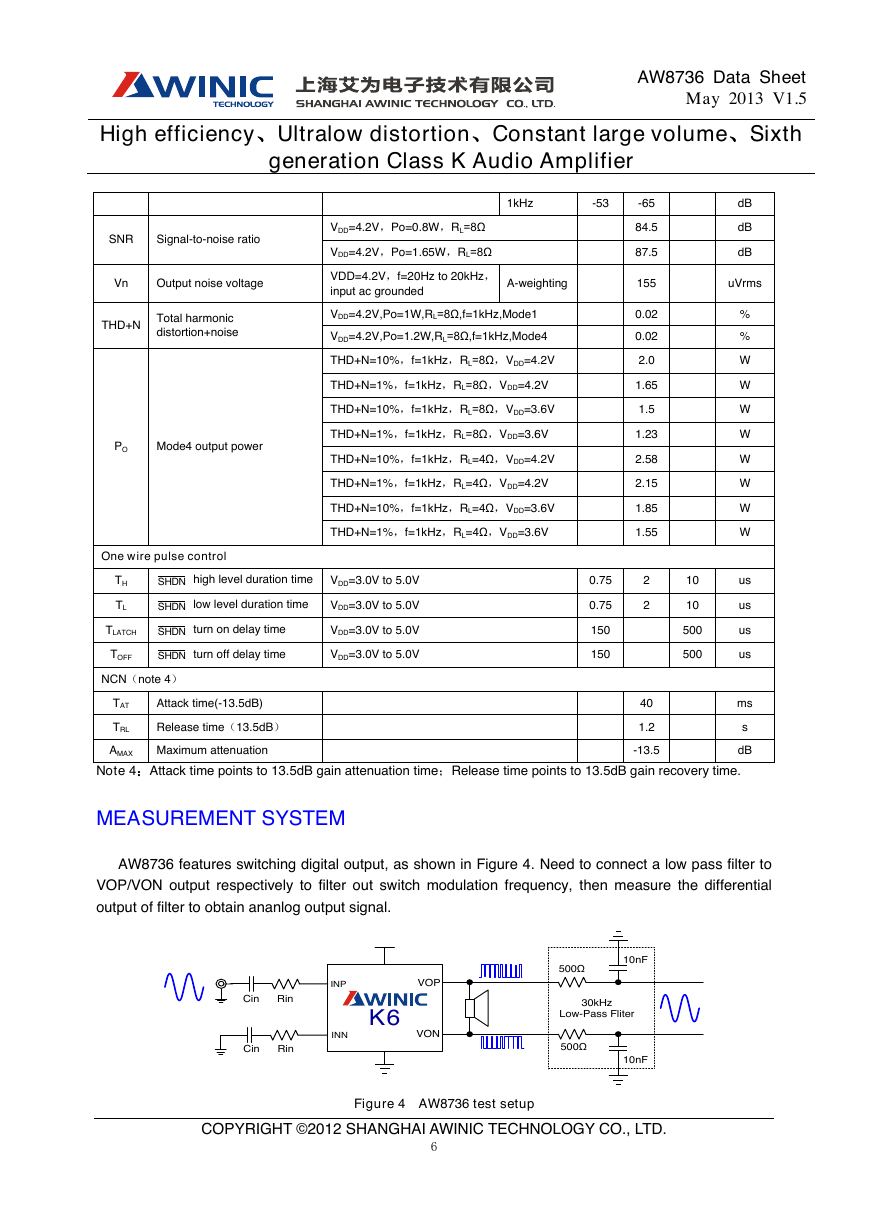
AW8736 features switching digital output, as shown in Figure 4. Need to connect a low pass filter to
VOP/VON output respectively to filter out switch modulation frequency, then measure the differential
output of filter to obtain ananlog output signal.
Figure 4 AW8736 test setup
COPYRIGHT ©2012 SHANGHAI AWINIC TECHNOLOGY CO., LTD.
6
SHDNSHDNSHDNSHDNVOPVONINPINNRinCinK6RinCin30kHzLow-Pass Fliter500Ω500Ω10nF10nF�
High efficiency、Ultralow distortion、Constant large volume、Sixth
generation Class K Audio Amplifier
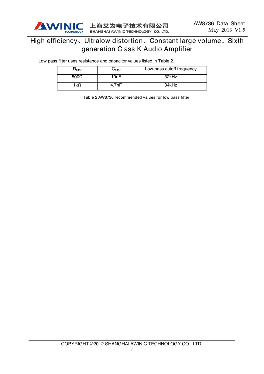
Low pass filter uses resistance and capacitor values listed in Table 2.
AW8736 Data Sheet
May 2013 V1.5
Rfilter
500Ω
1kΩ
Cfilter
10nF
4.7nF
Low-pass cutoff frequency
32kHz
34kHz
Table 2 AW8736 recommended values for low pass filter
COPYRIGHT ©2012 SHANGHAI AWINIC TECHNOLOGY CO., LTD.
7
�
High efficiency、Ultralow distortion、Constant large volume、Sixth
generation Class K Audio Amplifier
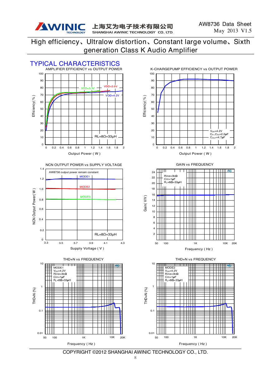
TYPICAL CHARACTERISTICS
AW8736 Data Sheet
May 2013 V1.5
COPYRIGHT ©2012 SHANGHAI AWINIC TECHNOLOGY CO., LTD.
8
00.20.40.60.81.01.23.33.53.94.3Supply Voltage ( V )NCN Output Power( W )NCN OUTPUT POWER vs SUPPLY VOLTAGE3.74.11.4RL=8Ω+33μHMODE1MODE2MODE3010203040506070809010000.20.40.60.811.21.41.61.82Output Power ( W )Efficiency( % )AMPLIFIER EFFICIENCY vs OUTPUT POWERRL=8Ω+33μHVDD=4.2VVDD=3.6VVDD=3.3V162424681012141820225010020K1K10KGAIN vs FREQUENCYFrequency ( Hz )Gain( V/V )010203040506070809010000.20.40.60.811.21.41.61.82Output Power ( W )Efficiency( % )K-CHARGEPUMP EFFICIENCY vs OUTPUT POWERVDD=4.2VCF1,CF2=2.2μFCOUT=4.7μFRine=3kΩCin=1μFRL=8Ω+33μH1100.10.01THD+N vs FREQUENCYTHD+N (%)Frequency ( Hz )5010020K1K10KMODE1VDD=4.2VRine=3kΩCin=1μFRL=8Ω+33μH1100.10.01THD+N vs FREQUENCYTHD+N (%)Frequency ( Hz )5010020K1K10KMODE2VDD=4.2VRine=3kΩCin=1μFRL=8Ω+33μHAW8736 output power remain constant�




 2023年江西萍乡中考道德与法治真题及答案.doc
 2012年重庆南川中考生物真题及答案.doc
 2013年江西师范大学地理学综合及文艺理论基础考研真题.doc
 2020年四川甘孜小升初语文真题及答案I卷.doc
 2020年注册岩土工程师专业基础考试真题及答案.doc
 2023-2024学年福建省厦门市九年级上学期数学月考试题及答案.doc
 2021-2022学年辽宁省沈阳市大东区九年级上学期语文期末试题及答案.doc
 2022-2023学年北京东城区初三第一学期物理期末试卷及答案.doc
 2018上半年江西教师资格初中地理学科知识与教学能力真题及答案.doc
 2012年河北国家公务员申论考试真题及答案-省级.doc
 2020-2021学年江苏省扬州市江都区邵樊片九年级上学期数学第一次质量检测试题及答案.doc
 2022下半年黑龙江教师资格证中学综合素质真题及答案.doc