logo资料库

Msp430x1xx family User's Guide.pdf

第1页 / 共414页
第2页 / 共414页
第3页 / 共414页
第4页 / 共414页
第5页 / 共414页
第6页 / 共414页
第7页 / 共414页
第8页 / 共414页
资料共414页,剩余部分请下载后查看
SLAU049F - MSP430x1xx Family
IMPORTANT NOTICE
Preface
Read This First
About This Manual
Related Documentation From Texas Instruments
FCC Warning
Notational Conventions
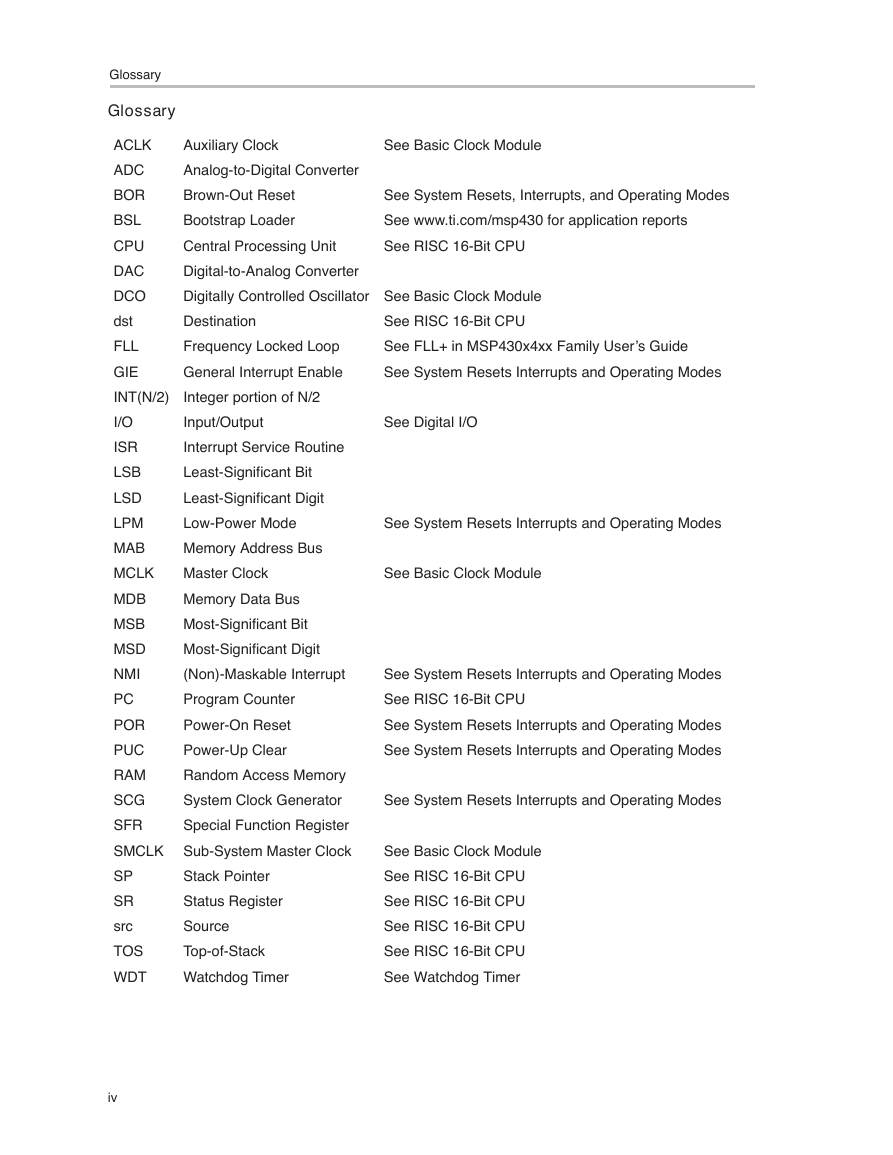
Glossary
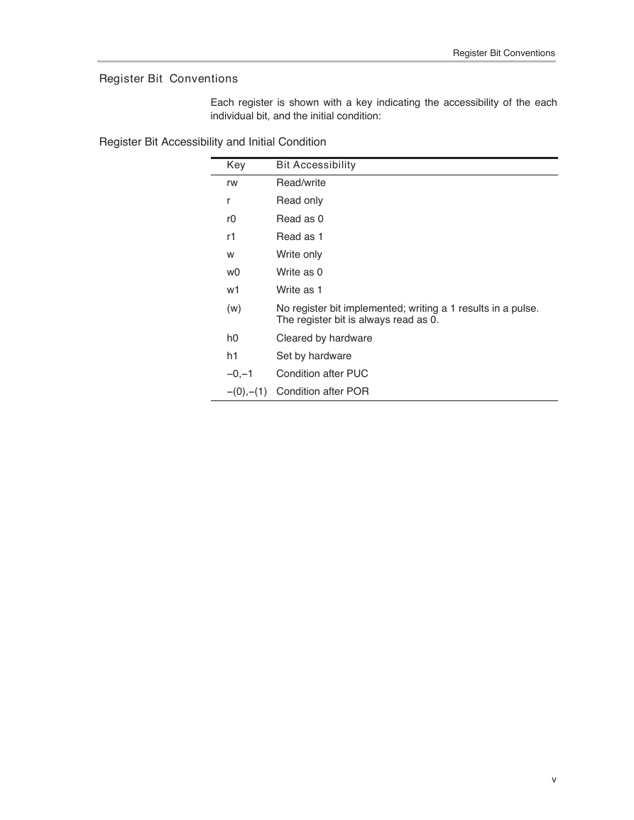
Register Bit Conversions
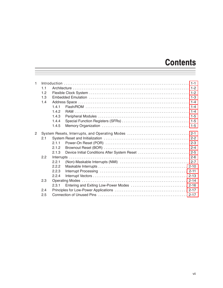
Contents
Chapter 1: Introduction
1.1 Architecture
1.2 Flexible Clock System
1.3 Embedded Emulation
1.4 Address Space
1.4.1 Flash/ROM
1.4.2 RAM
1.4.3 Peripheral Modules
1.4.4 Special Function Registers (SFRs)
1.4.5 Memory Organization
Chapter 2: System Resets, Interrupts, and Operating Modes
2.1 System Reset and Initialization
2.1.1 Power-On Reset (POR)
2.1.2 Brownout Reset (BOR)
2.1.3 Device Initial Conditions After System Reset
Software Initialization
2.2 Interrupts
2.2.1 (Non)-Maskable Interrupts (NMI)
Reset/NMI Pin
Flash Access Violation
Oscillator Fault
Example of an NMI Interrupt Handler
2.2.2 Maskable Interrupts
2.2.3 Interrupt Processing
Interrupt Acceptance
Return From Interrupt
Interrupt Nesting
2.2.4 Interrupt Vectors
2.3 Operating Modes
2.3.1 Entering and Exiting Low-Power Modes
Extended Time in Low-Power Modes
2.4 Principles for Low-Power Applications
2.5 Connection of Unused Pins
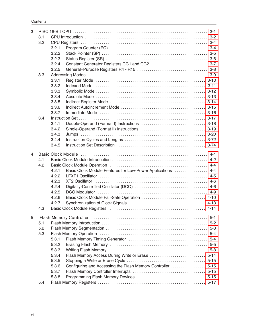
Chapter 3: RISC 16-Bit CPU
3.1 CPU Introduction
3.2 CPU Registers
3.2.1 Program Counter (PC)
3.2.2 Stack Pointer (SP)
3.2.3 Status Register (SR)
3.2.4 Constant Generator Registers CG1 and CG2
Constant Generator - Expanded Instruction Set
3.2.5 General-Purpose Registers R4 - R15
3.3 Addressing Modes
3.3.1 Register Mode
3.3.2 Indexed Mode
3.3.3 Symbolic Mode
3.3.4 Absolute Mode
3.3.5 Indirect Register Mode
3.3.6 Indirect Autoincrement Mode
3.3.7 Immediate Mode
3.4 Instruction Set
3.4.1 Double-Operand (Format I) Instructions
3.4.2 Single-Operand (Format II) Instructions
3.4.3 Jumps
3.4.4 Instruction Cycles and Lengths
Interrupt and Reset Cycles
Format-II (Single Operand) Instruction Cycles and Lengths
Format-III (Jump) Instruction Cycles and Lengths
Format-I (Double Operand) Instruction Cycles and Lengths
3.4.5 Instruction Set Description
Chapter 4: Basic Clock Module
4.1 Basic Clock Module Introduction
4.2 Basic Clock Module Operation
4.2.1 Basic Clock Module Features for Low-Power Applications
4.2.2 LFXT1 Oscillator
4.2.3 XT2 Oscillator
4.2.4 Digitally-Controlled Oscillator (DCO)
Disabling the DCO
Adjusting the DCO frequency
Using an External Resistor ( ROSC) for the DCO
4.2.5 DCO Modulator
4.2.6 Basic Clock Module Fail-Safe Operation
Oscillator Fault Detection
Sourcing MCLK from a Crystal
4.2.7 Synchronization of Clock Signals
4.3 Basic Clock Module Registers
DCOCTL, DCO Control Register
BCSCTL1, Basic Clock System Control Register 1
BCSCTL2, Basic Clock System Control Register 2
IE1, Interrupt Enable Register 1
IFG1, Interrupt Flag Register 1
Chapter 5: Flash Memory Controller
5.1 Flash Memory Introduction
5.2 Flash Memory Segmentation
5.3 Flash Memory Operation
5.3.1 Flash Memory Timing Generator
5.3.2 Erasing Flash Memory
Initiating an Erase from Within Flash Memory
Initiating an Erase from RAM
5.3.3 Writing Flash Memory
Byte/Word Write
Initiating a Byte/Word Write from Within Flash Memory
Initiating a Byte/Word Write from RAM
Block Write
Block Write Flow and Example
5.3.4 Flash Memory Access During Write or Erase
5.3.5 Stopping a Write or Erase Cycle
5.3.6 Configuring and Accessing the Flash Memory Controller
5.3.7 Flash Memory Controller Interrupts
5.3.8 Programming Flash Memory Devices
Programming Flash Memory via JTAG
Programming Flash Memory via the Bootstrap loader (BSL)
Programming Flash Memory via a Custom Solution
5.4 Flash Memory Registers
FCTL1, Flash Memory Control Register
FCTL2, Flash Memory Control Register
FCTL3, Flash Memory Control Register FCTL3
IE1, Interrupt Enable Register 1
Chapter 6: Supply Voltage Supervisor
6.1 SVS Introduction
6.2 SVS Operation
6.2.1 Configuring the SVS
6.2.2 SVS Comparator Operation
6.2.3 Changing the VLDx Bits
6.2.4 SVS Operating Range
6.3 SVS Registers
SVSCTL, SVS Control Register
Chapter 7: Hardware Multiplier
7.1 Hardware Multiplier Introduction
7.2 Hardware Multiplier Operation
7.2.1 Operand Registers
7.2.2 Result Registers
MACS Underflow and Overflow
7.2.3 Software Examples
7.2.4 Indirect Addressing of RESLO
7.2.5 Using Interrupts
7.3 Hardware Multiplier Registers
Chapter 8: DMA Controller
8.1 DMA Introduction
8.2 DMA Operation
8.2.1 DMA Addressing Modes
8.2.2 DMA Transfer Modes
Single Transfer
Block Transfers
Burst-Block Transfers
8.2.3 Initiating DMA Transfers
Edge-Sensitive Triggers
Level-Sensitive Triggers
Halting Executing Instructions for DMA Transfers
8.2.4 Stopping DMA Transfers
8.2.5 DMA Channel Priorities
8.2.6 DMA Transfer Cycle Time
8.2.7 Using DMA with System Interrupts
8.2.8 DMA Controller Interrupts
8.2.9 Using the I2C Module with the DMA Controller
8.2.10 Using ADC12 with the DMA Controller
8.2.11 Using DAC12 With the DMA Controller
8.3 DMA Registers
DMACTL0, DMA Control Register 0
DMACTL1, DMA Control Register 1
DMAxCTL, DMA Channel x Control Register
DMAxSA, DMA Source Address Register
DMAxDA, DMA Destination Address Register
DMAxSZ, DMA Size Address Register
Chapter 9: Digital I/O
9.1 Digital I/O Introduction
9.2 Digital I/O Operation
9.2.1 Input Register PxIN
9.2.2 Output Registers PxOUT
9.2.3 Direction Registers PxDIR
9.2.4 Function Select Registers PxSEL
9.2.5 P1 and P2 Interrupts
Interrupt Flag Registers P1IFG, P2IFG
Interrupt Edge Select Registers P1IES, P2IES
Interrupt Enable P1IE, P2IE
9.2.6 Configuring Unused Port Pins
9.3 Digital I/O Registers
Chapter 10: Watchdog Timer
10.1 Watchdog Timer Introduction
10.2 Watchdog Timer Operation
10.2.1 Watchdog Timer Counter
10.2.2 Watchdog Mode
10.2.3 Interval Timer Mode
10.2.4 Watchdog Timer Interrupts
10.2.5 Operation in Low-Power Modes
10.2.6 Software Examples
10.3 Watchdog Timer Registers
WDTCTL, Watchdog Timer Register
IE1, Interrupt Enable Register 1
IFG1, Interrupt Flag Register 1
Chapter 11: Timer_A
11.1 Timer_A Introduction
11.2 Timer_A Operation
11.2.1 16-Bit Timer Counter
Clock Source Select and Divider
11.2.2 Starting the Timer
11.2.3 Timer Mode Control
Up Mode
Continuous Mode
Use of the Continuous Mode
Up/Down Mode
Use of the Up/Down Mode
11.2.4 Capture/Compare Blocks
Capture Mode
Compare Mode
11.2.5 Output Unit
Output Modes
11.2.6 Timer_A Interrupts
TACCR0 Interrupt
TAIV, Interrupt Vector Generator
11.3 Timer_A Registers
TACTL, Timer_A Control Register
TAR, Timer_A Register
TACCTLx, Capture/Compare Control Register
TAIV, Timer_A Interrupt Vector Register
Chapter 12: Timer_B
12.1 Timer_B Introduction
12.1.1 Similarities and Differences From Timer_A
12.2 Timer_B Operation
12.2.1 16-Bit Timer Counter
TBR Length
Clock Source Select and Divider
12.2.2 Starting the Timer
12.2.3 Timer Mode Control
Up Mode
Continuous Mode
Use of the Continuous Mode
Up/Down Mode
Use of the Up/Down Mode
12.2.4 Capture/Compare Blocks
Capture Mode
Compare Mode
12.2.5 Output Unit
Output Modes
12.2.6 Timer_B Interrupts
TBIV, Interrupt Vector Generator
TBIV, Interrupt Handler Examples
12.3 Timer_B Registers
Timer_B Control Register TBCTL
TBR, Timer_B Register
TBCCTLx, Capture/Compare Control Register
TBIV, Timer_B Interrupt Vector Register
Chapter 13: USART Peripheral Interface, UART Mode
13.1 USART Introduction: UART Mode
13.2 USART Operation: UART Mode
13.2.1 USART Initialization and Reset
13.2.2 Character Format
13.2.3 Asynchronous Communication Formats
Idle-Line Multiprocessor Format
Address-Bit Multiprocessor Format
Automatic Error Detection
13.2.4 USART Receive Enable
13.2.5 USART Transmit Enable
13.2.6 UART Baud Rate Generation
Baud Rate Bit Timing
Determining the Modulation Value
Transmit Bit Timing
Receive Bit Timing
Typical Baud Rates and Errors
13.2.7 USART Interrupts
USART Transmit Interrupt Operation
USART Receive Interrupt Operation
Receive-Start Edge Detect Operation
13.3 USART Registers: UART Mode
UxCTL, USART Control Register
UxTCTL, USART Transmit Control Register
UxRCTL, USART Receive Control Register
UxBR0, USART Baud Rate Control Register 0
UxBR1, USART Baud Rate Control Register 1
UxMCTL, USART Modulation Control Register
UxRXBUF, USART Receive Buffer Register
UxTXBUF, USART Transmit Buffer Register
ME1, Module Enable Register 1
ME2, Module Enable Register 2
IE1, Interrupt Enable Register 1
IE2, Interrupt Enable Register 2
IFG1, Interrupt Flag Register 1
IFG2, Interrupt Flag Register 2
Chapter 14: USART Peripheral Interface, SPI Mode
14.1 USART Introduction: SPI Mode
14.2 USART Operation: SPI Mode
14.2.1 USART Initialization and Reset
14.2.2 Master Mode
Four-Pin SPI Master Mode
14.2.3 Slave Mode
Four-Pin SPI Slave Mode
14.2.4 SPI Enable
Transmit Enable
Receive Enable
14.2.5 Serial Clock Control
Serial Clock Polarity and Phase
14.2.6 SPI Interrupts
SPI Transmit Interrupt Operation
SPI Receive Interrupt Operation
14.3 USART Registers: SPI Mode
UxCTL, USART Control Register
UxTCTL, USART Transmit Control Register
UxRCTL, USART Receive Control Register
UxBR0, USART Baud Rate Control Register 0
UxBR1, USART Baud Rate Control Register 1
UxMCTL, USART Modulation Control Register
UxRXBUF, USART Receive Buffer Register
UxTXBUF, USART Transmit Buffer Register
ME1, Module Enable Register 1
ME2, Module Enable Register 2
IE1, Interrupt Enable Register 1
IE2, Interrupt Enable Register 2
IFG1, Interrupt Flag Register 1
IFG2, Interrupt Flag Register 2
Chapter 15: USART Peripheral Interface, I2C Mode
15.1 I2C Module Introduction
15.2 I2C Module Operation
15.2.1 I2C Module Initialization
15.2.2 I2C Serial Data
15.2.3 I2C Addressing Modes
7-Bit Addressing
10-Bit Addressing
Repeated START Conditions
15.2.4 I2C Module Operating Modes
Master Mode
Slave Mode
15.2.5 The I2C Data Register I2CDR
Transmit Underflow
Receive Overrun
15.2.6 I2C Clock Generation and Synchronization
15.2.7 Using the I2C Module with Low Power Modes
15.2.8 I2C Interrupts
I2CIV, Interrupt Vector Generator
15.3 I2C Module Registers
U0CTL, USART0 Control Register-I2C Mode
I2CTCTL, I2C Transmit Control Register
I2CDCTL, I2C Data Control Register
I2CDRW, I2CDRB, I2C Data Register
I2CNDAT, I2C Transfer Byte Count Register
I2CPSC, I2C Clock Prescaler Register
I2CSCLH, I2C Shift Clock High Register
I2CSCLL, I2C Shift Clock Low Register
I2COA, I2C Own Address Register, 7-Bit Addressing Mode
I2COA, I2C Own Address Register, 10-Bit Addressing Mode
I2CSA, I2C Slave Address Register, 7-Bit Addressing Mode
I2CSA, I2C Slave Address Register, 10-Bit Addressing Mode
I2CIE, I2C Interrupt Enable Register
I2CIFG, I2C Interrupt Flag Register
I2CIV, I2C Interrupt Vector Register
Chapter 16: Comparator_A
16.1 Comparator_A Introduction
16.2 Comparator_A Operation
16.2.1 Comparator
16.2.2 Input Analog Switches
16.2.3 Output Filter
16.2.4 Voltage Reference Generator
16.2.5 Comparator_A, Port Disable Register CAPD
16.2.6 Comparator_A Interrupts
16.2.7 Comparator_A Used to Measure Resistive Elements
16.3 Comparator_A Registers
CACTL1, Comparator_A Control Register 1
CACTL2, Comparator_A, Control Register
CAPD, Comparator_A, Port Disable Register
Chapter 17: ADC12
17.1 ADC12 Introduction
17.2 ADC12 Operation
17.2.1 12-Bit ADC Core
Conversion Clock Selection
17.2.2 ADC12 Inputs and Multiplexer
Analog Port Selection
17.2.3 Voltage Reference Generator
17.2.4 Auto Power-Down
17.2.5 Sample and Conversion Timing
Extended Sample Mode
Pulse Sample Mode
Sample Timing Considerations
17.2.6 Conversion Memory
17.2.7 ADC12 Conversion Modes
Single-Channel Single-Conversion Mode
Sequence-of-Channels Mode
Repeat-Single-Channel Mode
Repeat-Sequence-of-Channels Mode
Using the Multiple Sample and Convert (MSC) Bit
Stopping Conversions
17.2.8 Using the Integrated Temperature Sensor
17.2.9 ADC12 Grounding and Noise Considerations
17.2.10 ADC12 Interrupts
ADC12IV, Interrupt Vector Generator
ADC12 Interrupt Handling Software Example
17.3 ADC12 Registers
ADC12CTL0, ADC12 Control Register 0
ADC12CTL1, ADC12 Control Register 1
ADC12MEMx, ADC12 Conversion Memory Registers
ADC12MCTLx, ADC12 Conversion Memory Control Registers
ADC12IE, ADC12 Interrupt Enable Register
ADC12IFG, ADC12 Interrupt Flag Register
ADC12IV, ADC12 Interrupt Vector Register
Chapter 18: ADC10
18.1 ADC10 Introduction
18.2 ADC10 Operation
18.2.1 10-Bit ADC Core
Conversion Clock Selection
18.2.2 ADC10 Inputs and Multiplexer
18.2.3 Voltage Reference Generator
Internal Reference Low-Power Features
18.2.4 Auto Power-Down
18.2.5 Sample and Conversion Timing
Sample Timing Considerations
18.2.6 Conversion Modes
Single-Channel Single-Conversion Mode
Sequence-of-Channels Mode
Repeat-Single-Channel Mode
Repeat-Sequence-of-Channels Mode
Using the MSC Bit
Stopping Conversions
18.2.7 ADC10 Data Transfer Controller
One-Block Transfer Mode
Two-Block Transfer Mode
Continuous Transfer
DTC Transfer Cycle Time
18.2.8 Using the Integrated Temperature Sensor
18.2.9 ADC10 Grounding and Noise Considerations
18.2.10 ADC10 Interrupts
18.3 ADC10 Registers
ADC10CTL0, ADC10 Control Register 0
ADC10CTL1, ADC10 Control Register 1
ADC10AE, Analog (Input) Enable Control Register
ADC10MEM, Conversion-Memory Register, Binary Format
ADC10MEM, Conversion-Memory Register, 2’ s Complement Format
ADC10DTC0, Data Transfer Control Register 0
ADC10DTC1, Data Transfer Control Register 1
ADC10SA, Start Address Register for Data Transfer
Chapter 19: DAC12
19.1 DAC12 Introduction
19.2 DAC12 Operation
19.2.1 DAC12 Core
DAC12 Port Selection
19.2.2 DAC12 Reference
DAC12 Reference Input and Voltage Output Buffers
19.2.3 Updating the DAC12 Voltage Output
19.2.4 DAC12_xDAT Data Format
19.2.5 DAC12 Output Amplifier Offset Calibration
19.2.6 Grouping Multiple DAC12 Modules
19.2.7 DAC12 Interrupts
19.3 DAC12 Registers
DAC12_xCTL, DAC12 Control Register
DAC12_xDAT, DAC12 Data Register
MSP430x1xx Family User’s Guide 2006 Mixed Signal Products SLAU049F
IMPORTANT NOTICE Texas Instruments Incorporated and its subsidiaries (TI) reserve the right to make corrections, modifications, enhancements, improvements, and other changes to its products and services at any time and to discontinue any product or service without notice. Customers should obtain the latest relevant information before placing orders and should verify that such information is current and complete. All products are sold subject to TI’s terms and conditions of sale supplied at the time of order acknowledgment. TI warrants performance of its hardware products to the specifications applicable at the time of sale in accordance with TI’s standard warranty. Testing and other quality control techniques are used to the extent TI deems necessary to support this warranty. Except where mandated by government requirements, testing of all parameters of each product is not necessarily performed. TI assumes no liability for applications assistance or customer product design. Customers are responsible for their products and applications using TI components. To minimize the risks associated with customer products and applications, customers should provide adequate design and operating safeguards. TI does not warrant or represent that any license, either express or implied, is granted under any TI patent right, copyright, mask work right, or other TI intellectual property right relating to any combination, machine, or process in which TI products or services are used. Information published by TI regarding third-party products or services does not constitute a license from TI to use such products or services or a warranty or endorsement thereof. Use of such information may require a license from a third party under the patents or other intellectual property of the third party, or a license from TI under the patents or other intellectual property of TI. Reproduction of information in TI data books or data sheets is permissible only if reproduction is without alteration and is accompanied by all associated warranties, conditions, limitations, and notices. Reproduction of this information with alteration is an unfair and deceptive business practice. TI is not responsible or liable for such altered documentation. Resale of TI products or services with statements different from or beyond the parameters stated by TI for that product or service voids all express and any implied warranties for the associated TI product or service and is an unfair and deceptive business practice. TI is not responsible or liable for any such statements. Following are URLs where you can obtain information on other Texas Instruments products and application solutions: Products Amplifiers Data Converters DSP Interface Logic Power Mgmt Microcontrollers amplifier.ti.com dataconverter.ti.com dsp.ti.com interface.ti.com logic.ti.com power.ti.com microcontroller.ti.com Applications Audio Automotive Broadband Digital Control Military Optical Networking Security Telephony Video & Imaging Wireless www.ti.com/audio www.ti.com/automotive www.ti.com/broadband www.ti.com/digitalcontrol www.ti.com/military www.ti.com/opticalnetwork www.ti.com/security www.ti.com/telephony www.ti.com/video www.ti.com/wireless Mailing Address: Texas Instruments Post Office Box 655303 Dallas, Texas 75265 Copyright  2006, Texas Instruments Incorporated
Related Documentation From Texas Instruments Preface Read This First About This Manual This manual discusses modules and peripherals of the MSP430x1xx family of devices. Each discussion presents the module or peripheral in a general sense. Not all features and functions of all modules or peripherals are present on all devices. In addition, modules or peripherals may differ in their exact implementation between device families, or may not be fully implemented on an individual device or device family. Pin functions, internal signal connections and operational paramenters differ from device-to-device. The user should consult the device-specific datasheet for these details. Related Documentation From Texas Instruments For related documentation see the web site http://www.ti.com/msp430. FCC Warning This equipment is intended for use in a laboratory test environment only. It gen- erates, uses, and can radiate radio frequency energy and has not been tested for compliance with the limits of computing devices pursuant to subpart J of part 15 of FCC rules, which are designed to provide reasonable protection against radio frequency interference. Operation of this equipment in other en- vironments may cause interference with radio communications, in which case the user at his own expense will be required to take whatever measures may be required to correct this interference. Notational Conventions Program examples, are shown in a special typeface. iii
See System Resets, Interrupts, and Operating Modes See www.ti.com/msp430 for application reports See RISC 16-Bit CPU See RISC 16-Bit CPU See FLL+ in MSP430x4xx Family User’s Guide See System Resets Interrupts and Operating Modes See System Resets Interrupts and Operating Modes See Basic Clock Module See System Resets Interrupts and Operating Modes See RISC 16-Bit CPU See System Resets Interrupts and Operating Modes See System Resets Interrupts and Operating Modes See System Resets Interrupts and Operating Modes See Digital I/O See Basic Clock Module Auxiliary Clock Analog-to-Digital Converter Brown-Out Reset Bootstrap Loader Central Processing Unit Digital-to-Analog Converter Digitally Controlled Oscillator See Basic Clock Module Destination Frequency Locked Loop General Interrupt Enable Integer portion of N/2 Input/Output Interrupt Service Routine Least-Significant Bit Least-Significant Digit Low-Power Mode Memory Address Bus Master Clock Memory Data Bus Most-Significant Bit Most-Significant Digit (Non)-Maskable Interrupt Program Counter Power-On Reset Power-Up Clear Random Access Memory System Clock Generator Special Function Register Sub-System Master Clock Stack Pointer Status Register Source Top-of-Stack Watchdog Timer See Basic Clock Module See RISC 16-Bit CPU See RISC 16-Bit CPU See RISC 16-Bit CPU See RISC 16-Bit CPU See Watchdog Timer Glossary Glossary ACLK ADC BOR BSL CPU DAC DCO dst FLL GIE INT(N/2) I/O ISR LSB LSD LPM MAB MCLK MDB MSB MSD NMI PC POR PUC RAM SCG SFR SMCLK SP SR src TOS WDT iv
Register Bit Conventions Each register is shown with a key indicating the accessibility of the each individual bit, and the initial condition: Register Bit Accessibility and Initial Condition Register Bit Conventions Key rw r r0 r1 w w0 w1 (w) Bit Accessibility Read/write Read only Read as 0 Read as 1 Write only Write as 0 Write as 1 No register bit implemented; writing a 1 results in a pulse. The register bit is always read as 0. Cleared by hardware h0 Set by hardware h1 −0,−1 Condition after PUC −(0),−(1) Condition after POR v
vi
Contents Contents 1 Introduction 1.1 1.2 1.3 1.4 . . . . . . . . . . . . . . . . . . . . . . . . . . . . . . . . . . . . . . . . . . . . . . . . . . . . . . . . . . . . . . . . . . . . . . . . . . . . . . . . . . . . . . . . . . . . . . . . . . . . . . . . . . . . . . . . . . . . . . . . . . . . . . . . . . . . . . . . . . . . . . . . . . . . . . . . . . . . . . . . . . . . . . . . . . . . . . . . . . . . . . . . . . . . . . . . . . . . . . . . . . . . . . . . . . . . . . . . . . . . . . . . . . . . . . . . . . . . . . . . . . . . . . . . . . . . . . . . . . . . . . . . . . . . . . . . . . . . . . . . . . . . . . . . . . . . . . . . . . . . . . . . . . . . . . . . . . . . . . . . . . . . . . . . . . . . . . . . . . . . . . . . . . . . . . . . . . . . . . . . . . . . . . . . . . . . . . . . . . . . . . . . . . . . . . . . . . . . . . . . . . . . . . . . . . . . . . . . . . . . . . . . . . . . . . . . . . . . . . . . . . . . . . . . . . . . . . . . . . . . . . . . . . . . . . . . . . . . . . . . . . . . . . . . . . . . . . . . . . . . . . . . . . . . . . . . . . . . . . . . . . . . . . . . . . . . . . . . . . . . . . . . . . . . . . . . . . . . . . . Architecture Flexible Clock System Embedded Emulation Address Space 1.4.1 1.4.2 RAM 1.4.3 1.4.4 1.4.5 Memory Organization Peripheral Modules Special Function Registers (SFRs) Flash/ROM 1-1 1-2 1-2 1-3 1-4 1-4 1-4 1-5 1-5 1-5 2 System Resets, Interrupts, and Operating Modes (Non)-Maskable Interrupts (NMI) System Reset and Initialization Power-On Reset (POR) 2.1.1 2.1.2 Brownout Reset (BOR) 2.1.3 Device Initial Conditions After System Reset Interrupts 2.2.1 2.2.2 Maskable Interrupts Interrupt Processing 2.2.3 2.2.4 Interrupt Vectors Operating Modes 2.3.1 Principles for Low-Power Applications Connection of Unused Pins . . . . . . . . . . . . . . . . . . . . . . . . . . . . . . . . . . . . . . . . . . . . . . . . . . . . . . . . . . . . . . . . . . . . . . . . . . . . . . . . . . . . . . . . . . . . . . . . . . . . . . . . . . . . . . . . . . . . . . . . . . . . . . . . . . . . . . . . . . . . . . . . . . . . . . . . . . . . . . . . . . . . . . . . . . . . . . . . . . . . . . . . . . . . . . . . . . . . . . . . . . . . . . . . . . . . . . . . . . . . . . . . . . . . . . . . . . . . . . . . . . . . . . . . . . . . . . . . . . . . . . . . . . . . . . . . . . . . . . . . . . . . . . . . . . . . . . . . . . . . . . . . . . . . . . . . . . . . . . . . . . . . . . . . . . . . . . . . . . . . . . . . . . . . . . . . . . . . . . . . . . . . . . . . . . . . . . . . . . . . . . . . . . . . . . . . . . . . . . . . . . . . . . . . . . . . . . . . . . . . . . . . . . . . . . . . . . . . . . . . . . . . . . . . . . . . . . . . . . . . . . . . . . . . . . . . . . . . . . . . . . . . . . . . . . . . . . . . . . . . . . . . . . . . . . . . . . . . . . . . . . . . . . . . . . . . . . . . . . . . . . . . . . . . . . . . . . . . . . . . . . . . . . . . . . . . . . . . . . . . . . . . . . . . . . . . . . . . . . . . . . . . . . . . . . . . . . . . . . . . . . . . . . . . . . . . . Entering and Exiting Low-Power Modes 2-1 2-2 2-3 2-4 2-5 2-6 2-7 2-10 2-11 2-13 2-14 2-16 2-17 2-17 2.1 2.2 2.3 2.4 2.5 vii
Contents 3 RISC 16-Bit CPU 4 Basic Clock Module Program Counter (PC) Stack Pointer (SP) Status Register (SR) CPU Introduction CPU Registers 3.2.1 3.2.2 3.2.3 3.2.4 Constant Generator Registers CG1 and CG2 3.2.5 General−Purpose Registers R4 - R15 Addressing Modes 3.3.1 Register Mode Indexed Mode 3.3.2 Symbolic Mode 3.3.3 3.3.4 Absolute Mode Indirect Register Mode 3.3.5 Indirect Autoincrement Mode 3.3.6 3.3.7 Immediate Mode Instruction Set 3.4.1 Double-Operand (Format I) Instructions Single-Operand (Format II) Instructions 3.4.2 Jumps 3.4.3 3.4.4 Instruction Cycles and Lengths Instruction Set Description 3.4.5 . . . . . . . . . . . . . . . . . . . . . . . . . . . . . . . . . . . . . . . . . . . . . . . . . . . . . . . . . . . . . . . . . . . . . . . . . . . . . . . . . . . . . . . . . . . . . . . . . . . . . . . . . . . . . . . . . . . . . . . . . . . . . . . . . . . . . . . . . . . . . . . . . . . . . . . . . . . . . . . . . . . . . . . . . . . . . . . . . . . . . . . . . . . . . . . . . . . . . . . . . . . . . . . . . . . . . . . . . . . . . . . . . . . . . . . . . . . . . . . . . . . . . . . . . . . . . . . . . . . . . . . . . . . . . . . . . . . . . . . . . . . . . . . . . . . . . . . . . . . . . . . . . . . . . . . . . . . . . . . . . . . . . . . . . . . . . . . . . . . . . . . . . . . . . . . . . . . . . . . . . . . . . . . . . . . . . . . . . . . . . . . . . . . . . . . . . . . . . . . . . . . . . . . . . . . . . . . . . . . . . . . . . . . . . . . . . . . . . . . . . . . . . . . . . . . . . . . . . . . . . . . . . . . . . . . . . . . . . . . . . . . . . . . . . . . . . . . . . . . . . . . . . . . . . . . . . . . . . . . . . . . . . . . . . . . . . . . . . . . . . . . . . . . . . . . . . . . . . . . . . . . . . . . . . . . . . . . . . . . . . . . . . . . . . . . . . . . . . . . . . . . . . . . . . . . . . . . . . . . . . . . . . . . . . . . . . . . . . . . . . . . . . . . . . . . . . . . . . . . . . . . . . . . . . . . . . . . . . . . . . . . . . . . . . . . . . . . . . . . . . . . . . . . . . . . . . . . . . . . . . . . . . . . . . . . . . . . . . . . . . . . . . . . . . . . . . . . . . . . . . . . . . . . . . . . . . . . . . . . . . . . . . . . . . . . . . . . . . . . . . . . . . . . . . . . . . . . . . . . . . . . . . . . . . . . . . . . . . . . . . . . . . . . . . . . . . . . . . . . . . . . . . . . . . . . . . . . . . . . . . . . . . . . . . . . . . . . . . . . . . . . . . . . . . . . . . . . . . . . . . . . . . . . . . . . . . . . . . . . . . . . . . . . . . . . . . . . . . . . . . . . . . . . . . . . . . . . . . . . . . . . . . . . . . . . . . . . . . . . . . . . . . . . . . . . . . . . . . . . . . . . . . . . . . . . . . . . . . . . . . . . . . . . . . . . . . . . . . . . . . . . . . . . 3-1 3-2 3-4 3-4 3-5 3-6 3-7 3-8 3-9 3-10 3-11 3-12 3-13 3-14 3-15 3-16 3-17 3-18 3-19 3-20 3-72 3-74 Basic Clock Module Features for Low-Power Applications LFXT1 Oscillator XT2 Oscillator Basic Clock Module Introduction Basic Clock Module Operation 4.2.1 4.2.2 4.2.3 4.2.4 Digitally-Controlled Oscillator (DCO) 4.2.5 DCO Modulator 4.2.6 4.2.7 Basic Clock Module Registers . . . . . . . . . . . . . . . . . . . . . . . . . . . . . . . . . . . . . . . . . . . . . . . . . . . . . . . . . . . . . . . . . . . . . . . . . . . . . . . . . . . . . . . . . . . . . . . . . . . . . . . . . . . . . . . . . . . . . . . . . . . . . . . . . . . . . . . . . . . . . . . . . . . . . . . . . . . . . . . . . . . . . . . . . . . . . . . . . . . . . . . . . . . . . . . . . . . . . . . . . . . . . . . . . . . . . . . . . . . . . . . . . . . . . . . . . . . . . . . . . . . . . . . . . . . . . . . . . . . . . . . . . . . . . . . . . . . . . . . . . . . . . . . . . . . . . . . . . . . . . . . . . . . . . . . . . . . . . . . . . . . . . . . . . . . . . . . . . . . . . . . . . . . . . . . . . . . . . . . . . . . . . . . . . . . . . . . . . . . . . . . . . . . . . . . . . . . . . . . . . . . . . . . . . . . . . . . . . . . . . . . . . . . . . . . . . . . . . . . . . . . . . . . . . . . . . . . . . . . . . . . . . . . . . . . . . . . . . . . Basic Clock Module Fail-Safe Operation Synchronization of Clock Signals 4-1 4-2 4-4 4-4 4-5 4-6 4-6 4-9 4-10 4-13 4-14 3.1 3.2 3.3 3.4 4.1 4.2 4.3 Flash Memory Controller 5.1 5.2 5.3 Flash Memory Introduction Flash Memory Segmentation Flash Memory Operation 5.3.1 Flash Memory Timing Generator 5.3.2 Erasing Flash Memory 5.3.3 Writing Flash Memory 5.3.4 5.3.5 5.3.6 Configuring and Accessing the Flash Memory Controller 5.3.7 5.3.8 Flash Memory Registers . . . . . . . . . . . . . . . . . . . . . . . . . . . . . . . . . . . . . . . . . . . . . . . . . . . . . . . . . . . . . . . . . . . . . . . . . . . . . . . . . . . . . . . . . . . . . . . . . . . . . . . . . . . . . . . . . . . . . . . . . . . . . . . . . . . . . . . . . . . . . . . . . . . . . . . . . . . . . . . . . . . . . . . . . . . . . . . . . . . . . . . . . . . . . . . . . . . . . . . . . . . . . . . . . . . . . . . . . . . . . . . . . . . . . . . . . . . . . . . . . . . . . . . . . . . . . . . . . . . . . . . . . . . . . . . . . . . . . . . . . . . . . . . . . . . . . . . . . . . . . . . . . . . . . . . . . . . . . . . . . . . . . . . . . . . . . . . . . . . . . . . . . . . . . . . . . . . . . . . . . . . . . . . . . . . . . . . . . . . . . . . . . . . . . . . . . . . . . . . . . . . . . . . . . . . . . . . . . . . . . . . . . . . . . . . . . . . . . . . . . . . . . . . . . . . . . . . . . . . . . . . . . . . . . . . . . . . . . . . . . . . . . . . . . . . . . . . . . . . . . . . . . . . . . . . . . . . . . . . . . . . . . . . . . . . . . . . . . . . . . . . Flash Memory Access During Write or Erase Stopping a Write or Erase Cycle Flash Memory Controller Interrupts Programming Flash Memory Devices 5-1 5-2 5-3 5-4 5-4 5-5 5-8 5-14 5-15 5-15 5-15 5-15 5-17 5.4 5 viii
分享到:
收藏