logo资料库

Analog Design and Simulation Using OrCAD Capture and PSpice.pdf

第1页 / 共320页
第2页 / 共320页
第3页 / 共320页
第4页 / 共320页
第5页 / 共320页
第6页 / 共320页
第7页 / 共320页
第8页 / 共320页
资料共320页,剩余部分请下载后查看
Analog Design and Simulation using OrCAD Capture and PSpice
Copyright
Preface
Instructions
Limits of OrCAD Demo CD
Pre-16.5
Post-16.5
1 Getting Started
1.1 Starting Capture
1.2 Creating a PSpice Project
1.3 Symbols and Parts
1.3.1 Symbols
1.3.2 Parts
1.4 Design Templates
1.5 Summary
1.6 Exercises
Exercise 1
Exercise 2
1.7 Extra Library Work
2 DC Bias Point Analysis
2.1 Netlist Generation
2.2 Displaying Bias Points
2.3 Save Bias Point
2.4 Load Bias Point
2.5 Exercises
Exercise 1
3 DC Analysis
3.1 DC Voltage Sweep
3.2 Markers
3.3 Exercises
Exercise 1
Exercise 2
4 AC Analysis
4.1 Simulation Parameters
4.2 AC Markers
4.3 Exercises
Exercise 1
Twin T notch filter
5 Parametric Sweep
5.1 Property Editor
5.2 Exercises
Exercise 1
Theory
Exercise 2
Notch Filter
Exercise 3
Active Notch Filter
6 Stimulus Editor
6.1 Stimulus Editor Transient Sources
6.1.1 Exponential 䔀砀瀀 Source
6.1.2 Pulse Source
6.1.3 VPWL
6.1.4 SIN 匀椀渀甀猀漀椀搀愀氀
6.1.5 SSFM 匀椀渀最氀攀ⴀ昀爀攀焀甀攀渀挀礀 䘀䴀
6.2 User-generated Time–Voltage Waveforms
6.3 Simulation Profiles
6.4 Exercise
7 Transient Analysis
7.1 Simulation Settings
7.2 Scheduling
7.3 Check Points
7.4 Defining a Time–Voltage Stimulus using Text Files
7.5 Exercises
Exercise 1
Exercise 2
Using The Graphically Created Waveform In The Stimulus Editor
Using A File With Timeevoltage Data Describing The Input Wave Form
Generating A Periodic Vin
8 Convergence Problems and Error Messages
8.1 Common Error Messages
8.2 Establishing a Bias Point
8.3 Convergence Issues
8.4 Simulation Settings Options
8.5 Exercises
Exercise 1
Exercise 2
Exercise 3
Exercise 4
9 Transformers
9.1 Linear Transformer
9.2 Non-linear Transformer
9.3 Predefined Transformers
9.4 Exercises
Exercise 1
Exercise 2
10 Monte Carlo Analysis
10.1 Simulation Settings
Output Variable
Number Of Runs
Use Distribution
Random Number Seed
Save Data From
Mc Load/Save
More Settings
10.2 Adding Tolerance Values
10.3 Exercises
Exercise 1
Exercise 2
Filter Specifications
11 Worst Case Analysis
11.1 Sensitivity Analysis
11.2 Worst Case Analysis
11.3 Adding Tolerances
11.4 Collating Functions
11.5 Exercise
12 Performance Analysis
12.1 Measurement Functions
12.2 Measurement Definitions
12.3 Exercises
Exercise 1
Exercise 2
13 Analog Behavioral Models
13.1 ABM devices
13.2 Exercises
Exercise 1
Exercise 2
14 Noise Analysis
14.1 Noise Types
14.1.1 Resistor Noise
14.1.2 Semiconductor Noise
14.2 Total Noise Contributions
14.3 Running a Noise Analysis
14.4 Noise Definitions
14.5 Exercise
15 Temperature Analysis
15.1 Temperature Coefficients
15.2 Running a Temperature Analysis
15.3 Exercises
Exercise 1
Exercise 2
16 Adding and Creating PSpice Models
16.1 Capture Properties for a PSpice Part
16.2 PSpice Model Definition
16.3 Subcircuits
16.4 Model Editor
16.4.1 Copying an Existing PSpice Model
16.4.2 Model Import Wizard
16.4.3 Downloading Models from a Vendor Website
16.4.4 Encryption
16.5 Exercises
Exercise 1
Exercise 2
Exercise 3
Exercise 4
Exercise 5
17 Transmission Lines
17.1 Ideal Transmission Lines
17.2 Lossy Transmission Lines
17.3 Exercises
Exercise 1
Matched Load for RL
RL replaced With a Short Circuit
RL Replaced With an Open Circuit
Exercise 2
Standing Wave Ratio SWR
SWR for Short Circuit
SWR for Open Circuit
18 Digital Simulation
18.1 Digital Device Models
18.2 Digital Circuits
18.3 Digital Simulation Profile
18.4 Displaying Digital Signals
18.5 Exercises
Exercise 1
Exercise 2
Exercise 3
19 Mixed Simulation
19.1 Exercises
Exercise 1
Exercise 2
20.1 Hierarchical Ports and Off-page Connectors
20.2 Hierarchical Blocks and Symbols
20.2.1 Hierarchical Blocks
20.2.2 Hierarchical Symbols
20.3 Passing Parameters
20.4 Hierarchical Netlist
20.5 Exercises
Exercise 1
Exercise 2
Creating a Hierarchical Symbol which can be Saved to a Library
Exercise 3
Testing the Oscillator in a Hierarchy
Exercise 4
Exercise 5
21 Magnetic Parts Editor
21.1 Design Cycle
21.2 Exercises
Exercise 1
Step 1: Component Selection
Step 2: General Information
Step 3: Electrical Parameters
Step 4: Core Selection
Step 5: Bobbin-Winding Selection
Step 6: Results View
Exercise 2
Creating a Transformer Model
Exercise 3
22 Test Benches
22.1 Selection of Test Bench Parts
22.2 Unconnected Floating Nets
22.3 Comparing and Updating Differences between the Master Design and Test Bench Designs
22.4 Exercises
Exercise 1
Exercise 2
Appendix PSpice Measurement Definitions
Index
0-9
A
B
C
D
E
F
G
H
I
J
K
L
M
N
O
P
Q
R
S
T
U
V
W
X
Y
Z
Analog Design and Simulation using OrCAD Capture and PSpice Dennis Fitzpatrick AMSTERDAM  BOSTON  HEIDELBERG  LONDON  NEW YORK  OXFORD PARIS  SAN DIEGO  SAN FRANCISCO  SINGAPORE  SYDNEY  TOKYO Newnes is an imprint of Elsevier
Newnes is an imprint of Elsevier The Boulevard, Langford Lane, Kidlington, Oxford, OX5 1GB, UK 225 Wyman Street, Waltham, MA 02451, USA First published 2012 Copyright Ó 2012 Elsevier Ltd. All rights reserved. No part of this publication may be reproduced or transmitted in any form or by any means, electronic or mechanical, including photocopying, recording, or any information storage and retrieval system, without permission in writing from the publisher. Details on how to seek permission, further information about the Publisher’s permissions policies and our arrangement with organizations such as the Copyright Clearance Center and the Copyright Licensing Agency, can be found at our website: www.elsevier.com/permissions This book and the individual contributions contained in it are protected under copyright by the Publisher (other than as may be noted herein). Notices Knowledge and best practice in this field are constantly changing. As new research and experience broaden our understanding, changes in research methods, professional practices, or medical treatment may become necessary. Practitioners and researchers must always rely on their own experience and knowledge in evaluating and using any information, methods, compounds, or experiments described herein. In using such information or methods they should be mindful of their own safety and the safety of others, including parties for whom they have a professional responsibility. To the fullest extent of the law, neither the Publisher nor the authors, contributors, or editors, assume any liability for any injury and/or damage to persons or property as a matter of products liability, negligence or otherwise, or from any use or operation of any methods, products, instructions, or ideas contained in the material herein. British Library Cataloguing in Publication Data A catalogue record for this book is available from the British Library Library of Congress Control Number: 2011933640 ISBN: 978-0-08-097095-0 For information on all Newnes publications visit our website at www.elsevierdirect.com Printed and bound in the United Kingdom 12 13 14 15 10 9 8 7 6 5 4 3 2 1
Preface ix The Cadence/OrCAD family of Electronic Design Automation (EDA) software provides a complete design flow from schematic entry to circuit simulation through to PCB layout. The circuit is drawn using the Capture or Capture CIS schematic editor and circuit simulations are performed using PSpice. The schematic diagram is translated into a printed circuit board design using Cadence Allegro or PCB Editor which has replaced OrCAD Layout. The book has been written using the latest 16.5 software release and can be used with previous software releases and the evaluation demo CD. This book will benefit anybody with an interest in using the Cadence/OrCAD professional simulation software for the design and analysis of electronic circuits. The book provides a practical hands on approach to using the software and at the end of each chapter there are exercises with step by step instructions to complete. Thanks are due to the technical staff at the University of West London, Keith Pamment and Seth Thomas for reviewing the simulation exercises, Taranjit Kukal and Alok Tripathi from Cadence for reviewing the technical aspects of the book and Parallel-Systems UK for their support.
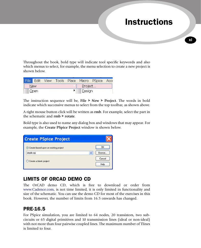
Instructions xi Throughout the book, bold type will indicate tool specific keywords and also which menus to select, for example, the menu selection to create a new project is shown below. The instruction sequence will be, File > New > Project. The words in bold indicate which successive menus to select from the top toolbar, as shown above. A right mouse button click will be written as rmb. For example, select the part in the schematic and rmb > rotate. Bold type is also used to name any dialog box and windows that may appear. For example, the Create PSpice Project window is shown below. LIMITS OF ORCAD DEMO CD The OrCAD demo CD, which is from www.Cadence.com, is not time limited, it is only limited in functionality and size of the schematic. You can use the demo CD for most of the exercises in this book. However, the number of limits from 16.5 onwards has changed. free to download or order PRE-16.5 For PSpice simulation, you are limited to 64 nodes, 20 transistors, two sub- circuits or 65 digital primitives and 10 transmission lines (ideal or non-ideal) with not more than four pairwise coupled lines. The maximum number of Tlines is limited to four.
xii Instructions The internal subcircuit nodes for opamps count towards the total node count. So use the uA741 from the eval library on the demo CD, which has 19 internal nodes. For digital circuits, the maximum number of nodes is limited to 250. In Capture you can create and view designs but cannot save designs that have more than 64 nets or 60 parts. The Capture CIS demo database is limited to 10 parts. You cannot create parts with more than 14 pins and you cannot save part libraries with more than 15 parts. The Model Editor is limited to diode models and the Model Import Wizard only supports two pin parts and models. The Stimulus Editor is limited to sine waves and digital clocks. Only simulation data created in the demo version can be displayed. The Magnetic Parts Editor can only be used to design power transformers. The Magnetic Parts Editor supplied database cannot be edited and only contains a single magnetic core. POST-16.5 From 16.5 onwards, for PSpice simulation, the number of nodes has increased to 75 nodes and there is no subcircuit limit. There is no limit to stimulus generation using the Stimulus Editor. In Capture you can create and view designs but cannot save designs that have more than 75 nets or 60 parts. You cannot have more than 1000 parts in the CIS database. You cannot create parts with more than 100 pins.
CHAPTER 1 Getting Started 1 Chapter Outline 1.1 Starting Capture 1 1.2 Creating a PSpice Project 2 1.3 Symbols and Parts 7 1.3.1 Symbols 7 1.3.2 Parts 8 1.4 Design Templates 10 1.5 Summary 12 1.6 Exercises 13 Exercise 1 13 Exercise 2 15 1.7 Extra Library Work 17 Those of you who are familiar with setting up projects and drawing schematics in Capture may want to skip this chapter, as it has been written for those of you who have little or no experience of using Capture. This chapter will describe how to start Capture and how to set up the project type and libraries for PSpice simulation. At the end of each chapter there are some exercises to do and as you go through the book, each chapter will build upon the exercises from previous chapters. 1.1 STARTING CAPTURE Circuit diagrams for PSpice simulation are drawn in either Capture or Capture CIS schematic editor. The CIS option, which stands for Component Information System, allows you to select and place components from a component database instead of selecting and placing components from a library. For this book, it does not matter whether the circuits are drawn in Capture or Capture CIS. If you have the OrCAD software installed, launch Capture or Capture CIS, by clicking on: Start > Program Files > OrCAD xx.x > Capture or Start > Program Files > OrCAD xx.x > Capture CIS Analog Design and Simulation using OrCAD Capture and PSpice. DOI: 10.1016/B978-0-08-097095-0.00001-5 Copyright Ó 2012 Elsevier Ltd. All rights reserved.
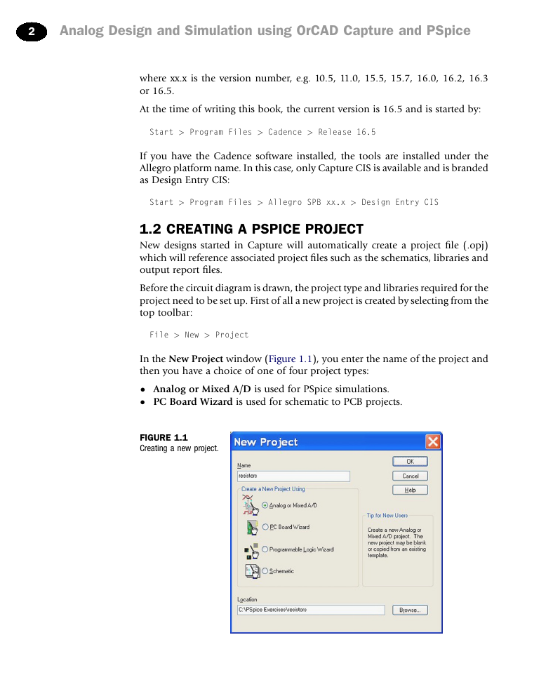
2 Analog Design and Simulation using OrCAD Capture and PSpice where xx.x is the version number, e.g. 10.5, 11.0, 15.5, 15.7, 16.0, 16.2, 16.3 or 16.5. At the time of writing this book, the current version is 16.5 and is started by: Start > Program Files > Cadence > Release 16.5 If you have the Cadence software installed, the tools are installed under the Allegro platform name. In this case, only Capture CIS is available and is branded as Design Entry CIS: Start > Program Files > Allegro SPB xx.x > Design Entry CIS 1.2 CREATING A PSPICE PROJECT New designs started in Capture will automatically create a project file (.opj) which will reference associated project files such as the schematics, libraries and output report files. Before the circuit diagram is drawn, the project type and libraries required for the project need to be set up. First of all a new project is created by selecting from the top toolbar: File > New > Project In the New Project window (Figure 1.1), you enter the name of the project and then you have a choice of one of four project types:  Analog or Mixed A/D is used for PSpice simulations.  PC Board Wizard is used for schematic to PCB projects. FIGURE 1.1 Creating a new project.
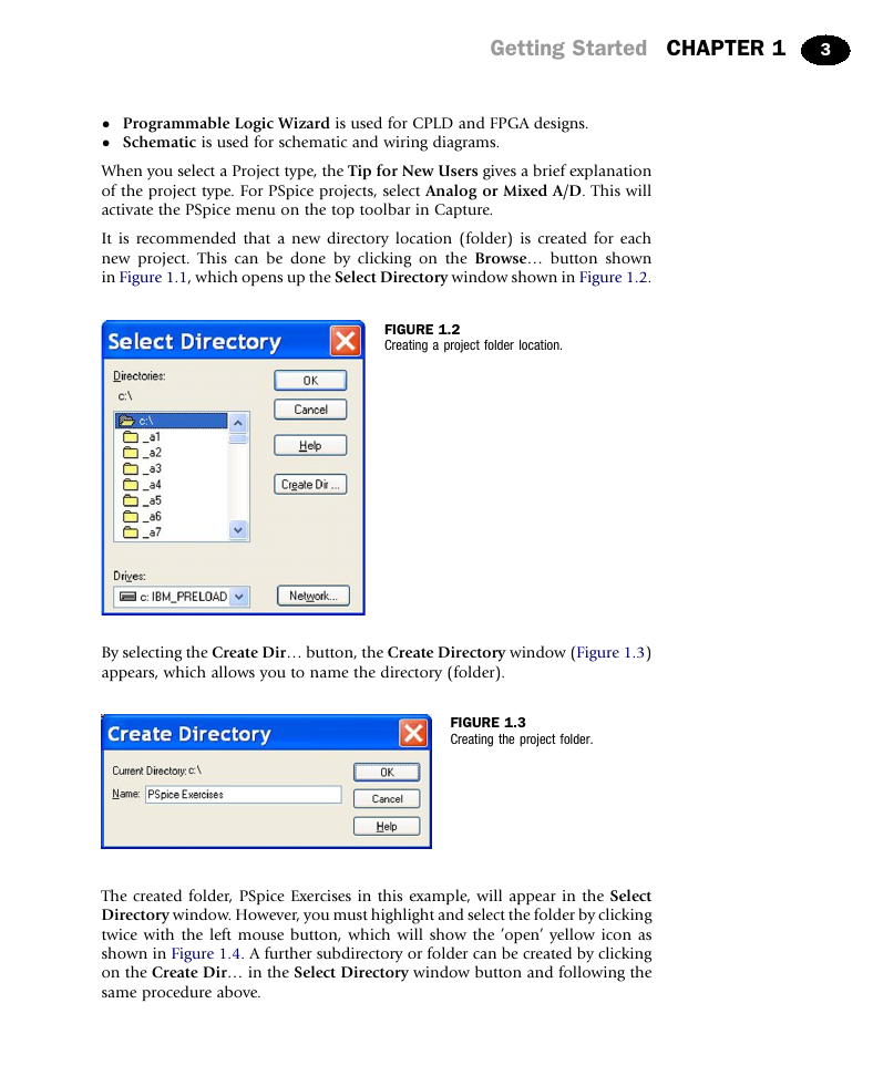
Getting Started CHAPTER 1 3  Programmable Logic Wizard is used for CPLD and FPGA designs.  Schematic is used for schematic and wiring diagrams. When you select a Project type, the Tip for New Users gives a brief explanation of the project type. For PSpice projects, select Analog or Mixed A/D. This will activate the PSpice menu on the top toolbar in Capture. It is recommended that a new directory location (folder) is created for each new project. This can be done by clicking on the Browse. button shown in Figure 1.1, which opens up the Select Directory window shown in Figure 1.2. FIGURE 1.2 Creating a project folder location. By selecting the Create Dir. button, the Create Directory window (Figure 1.3) appears, which allows you to name the directory (folder). FIGURE 1.3 Creating the project folder. The created folder, PSpice Exercises in this example, will appear in the Select Directory window. However, you must highlight and select the folder by clicking twice with the left mouse button, which will show the ’open’ yellow icon as shown in Figure 1.4. A further subdirectory or folder can be created by clicking on the Create Dir. in the Select Directory window button and following the same procedure above.
分享到:
收藏