Carbon-Nanotube Through-Silicon Via Interconnects for
Three-Dimensional Integration
Teng Wang , Kejll Jeppson , Lilei Ye , and Johan Liu *
Carbon Nanotubes
Continuous miniaturization and performance promotion of
electronics can be achieved by both the downscaling of on-
chip transistors and the progress of packaging technology.
High-density integration at the system level, supported by
advanced packaging solutions, is expected to be the main
driving force for the future shrinking of electronics. [ 1 ] One
recent focus in the fi eld of electronics packaging is the ver-
tical stacking of integrated circuits (ICs) to form three-
dimensional (3D) integration, [ 2 ] which offers some important
advantages. First, a much higher integration density can be
obtained by stacking multiple ICs on the footprint of only one
chip. Second, 3D integration signifi cantly shortens the lengths
of interconnects between different components, thus reducing
signal delays in a system. Furthermore, this technology allows
heterogeneous integration of various components onto a
system-on-package platform to achieve a complete functional
unit in a tiny space.
A central task in developing 3D integration is to build
reliable and effi cient electrical interconnects for signal
transfer and power distribution among the stacked layers.
Although conventional wire-bonding technology has already
been applied for this purpose, [ 3 ] a higher integration density
and input/output counts can only be achieved by through-
silicon via (TSV) interconnects. Besides 3D integration, the
TSV is also a favorable choice in some sensing applications
where a direct connection to the sensing side is needed. [ 4 , 5 ]
While there are a number of mature etching techniques
widely available to create high-aspect-ratio vias in silicon,
deep reactive-ion etching (DRIE) being the most prominent
example, the major diffi culty in TSV development lies in the
fi lling of a conductive material in deep vias, as well as their
interconnection and insulation.
T. Wang , Prof. K. Jeppson , Prof. J. Liu
Department of Microtechnology and Nanoscience (MC2)
Chalmers University of Technology
412 96 Göteborg, Sweden
E-mail: johan.liu@chalmers.se
Dr. L. Ye
SHT Smart High-Tech AB
Fysikgränd 3, 412 96 Göteborg, Sweden
Prof. J. Liu
Key Laboratory of New Displays and System Applications and SMIT Center
School of Mechanical Engineering and Automation
Shanghai University
Box 282, No. 149 Yanchang Road, 200072 Shanghai, China
DOI: 10.1002/smll.201100615
The most common method to fi ll TSVs is electroplating
of copper, [ 6 , 7 ] the reliability of which is, however, a serious
concern. [ 8 , 9 ] The manufacturability of Cu-fi lled TSVs is also
a barrier towards their successful application due to highly
demanding fabrication processes, such as seed and barrier
layer deposition in high-aspect-ratio vias. [ 10 ] Some other
materials, such as tungsten and polysilicon, [ 11 , 12 ] have also
been used as via fi lling materials but all have limitations in
reliability, manufacturability, and performance. Therefore
there is a strong need to fi nd alternative materials for TSV
fi lling.
Carbon nanotubes (CNTs) were proposed as a pro mising
material to build future interconnects due to their many
attractive properties. CNTs are mechanically fl exible and
resilient, [ 13 ] and have very low thermal expansion. [ 14 ] The
current-carrying capacity of CNTs can be up to 10 9 A cm − 2 ,
much higher than that of copper. [ 15 ] CNTs do not easily fail
due to electromigration and have very low Joule heating. [ 16 , 17 ]
Moreover, they are thermally conductive and stable. [ 18 , 19 ]
Whereas these advantages triggered intensive research on
developing CNT-based via interconnects, [ 20 ] the majority of
effort focuses on on-chip interconnection. Reports on CNT-
based TSVs, much deeper and normally with higher aspect
ratios, are comparatively limited. Two recent modeling works
predicted superior performance of CNT-based TSVs com-
pared to Cu-fi lled ones. [ 21 , 22 ] Experimental progress was
reported but still at a preliminary stage, without any assembly
processes after CNT growth. [ 23 , 24 ]
Herein, an easy-to-implement scheme for interconnecting
CNT-based TSVs in stacked structures for 3D integration is
demonstrated. There are two scenarios in interconnecting
TSVs, namely connecting one TSV to another and connecting
a TSV to a metal pad or line, both of which are addressed in
this work.
The vias were etched in Si by a standard DRIE process.
The CNT forests were directly grown by thermal chemical
vapor deposition (CVD) from a predeposited catalyst layer
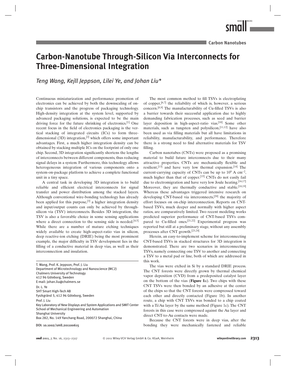
on the bottom of the vias ( Figure 1 a). Two chips with these
CNT TSVs were then bonded by an adhesive at the center
of the chips so that the CNT forests were compressed toward
each other and directly contacted (Figure 1 b). In another
route, a chip with CNT TSVs was bonded to a chip coated
with a Ti/Au layer by the same method (Figure 1 c). The CNT
forests in this case were compressed against the Au layer and
direct CNT-to-Au contacts were made.
Because the CNT forests were in deep vias, after the
bonding they were mechanically fastened and reliable
small 2011, 7, No. 16, 2313–2317
© 2011 Wiley-VCH Verlag GmbH & Co. KGaA, Weinheim
wileyonlinelibrary.com
2313
�
communications
(a)
(b)
(c)
CNTs Si
(d)
(e)
(f)
Configuration 1
Configuration 2
Configuration 3
Adhesive
Ti/Au
Figure 1 . Illustrations of the interconnection of CNT TSVs and the
fabricated test confi gurations. a) CNT forests were grown from the
bottom of deep vias in silicon. b) Two chips with CNT-fi lled TSVs
were stacked face-to-face by an adhesive applied at the center of the
chips. c) One chip with CNT-fi lled TSVs was bonded to a substrate
covered with a Ti/Au layer by an adhesive at the center of the chip.
d) Continued from the structure in (a) with the CNT forests controlled to
just reach the top Si surface during growth, a Ti/Au layer was sputtered
onto the top surface and the Si was dry etched from the back to expose
the bottom of the CNT forests. e) Continued from the structure in (b),
a similar process as in (d) was performed to expose the CNT forests.
f) Continued from the structure in (c), the Si was dry etched to expose
the CNT forests.
contacts were made. While macroscale direct CNT-to-CNT
and carbon nanofi ber (CNF)-to-CNF contacts for both
electrical and mechanical connections have already been
reported, [ 25 , 26 ] we realized such contacts on a microscale in
the present work.
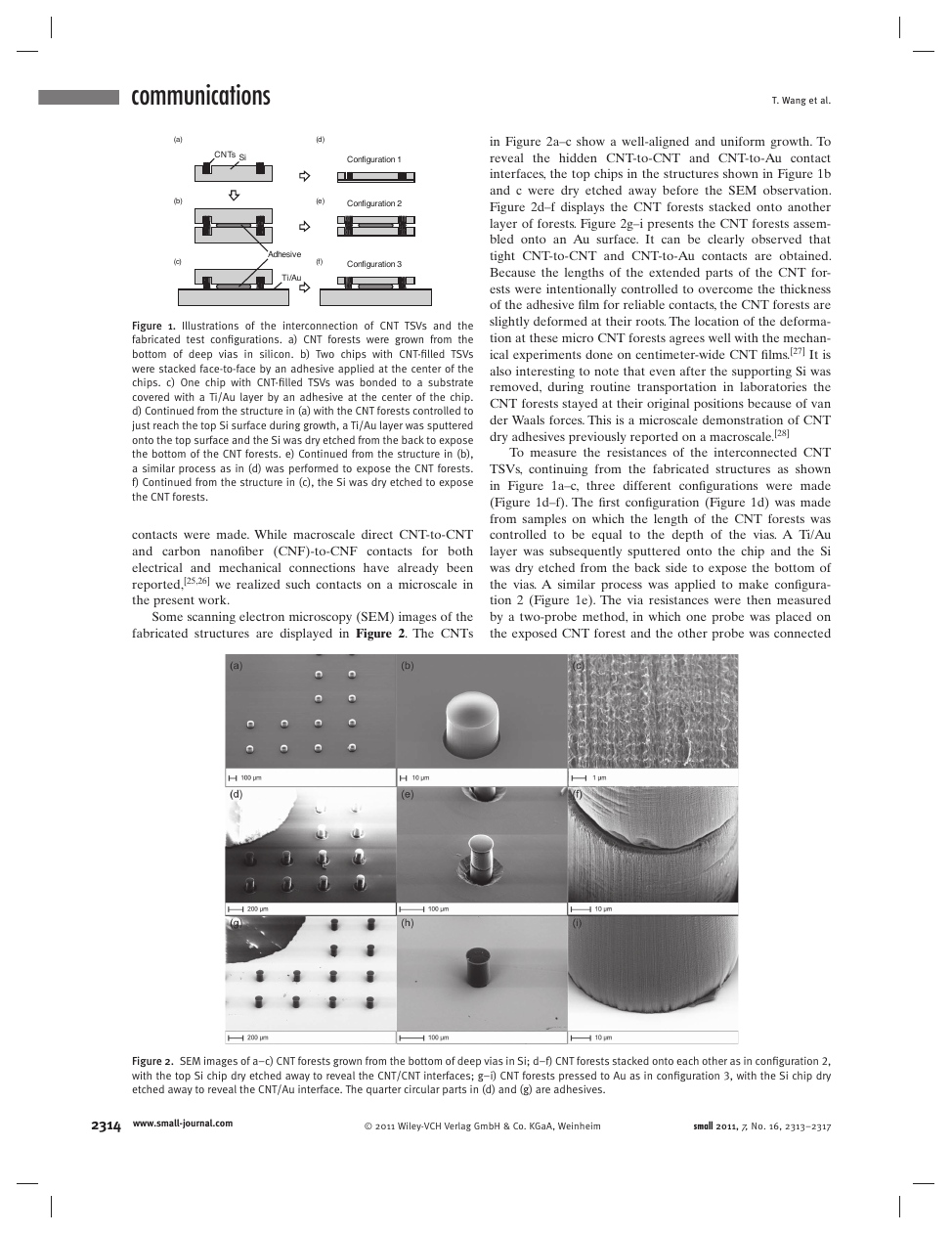
Some scanning electron microscopy (SEM) images of the
fabricated structures are displayed in Figure 2 . The CNTs
T. Wang et al.
in Figure 2 a–c show a well-aligned and uniform growth. To
reveal the hidden CNT-to-CNT and CNT-to-Au contact
interfaces, the top chips in the structures shown in Figure 1 b
and c were dry etched away before the SEM observation.
Figure 2 d–f displays the CNT forests stacked onto another
layer of forests. Figure 2 g–i presents the CNT forests assem-
bled onto an Au surface. It can be clearly observed that
tight CNT-to-CNT and CNT-to-Au contacts are obtained.
Because the lengths of the extended parts of the CNT for-
ests were intentionally controlled to overcome the thickness
of the adhesive fi lm for reliable contacts, the CNT forests are
slightly deformed at their roots. The location of the deforma-
tion at these micro CNT forests agrees well with the mechan-
ical experiments done on centimeter-wide CNT fi lms. [ 27 ] It is
also interesting to note that even after the supporting Si was
removed, during routine transportation in laboratories the
CNT forests stayed at their original positions because of van
der Waals forces. This is a microscale demonstration of CNT
dry adhesives previously reported on a macroscale. [ 28 ]
To measure the resistances of the interconnected CNT
TSVs, continuing from the fabricated structures as shown
in Figure 1 a–c, three different confi gurations were made
(Figure 1 d–f). The fi rst confi guration (Figure 1 d) was made
from samples on which the length of the CNT forests was
controlled to be equal to the depth of the vias. A Ti/Au
layer was subsequently sputtered onto the chip and the Si
was dry etched from the back side to expose the bottom of
the vias. A similar process was applied to make confi gura-
tion 2 (Figure 1 e). The via resistances were then measured
by a two-probe method, in which one probe was placed on
the exposed CNT forest and the other probe was connected
Figure 2 . SEM images of a–c) CNT forests grown from the bottom of deep vias in Si; d–f) CNT forests stacked onto each other as in confi guration 2,
with the top Si chip dry etched away to reveal the CNT/CNT interfaces; g–i) CNT forests pressed to Au as in confi guration 3, with the Si chip dry
etched away to reveal the CNT/Au interface. The quarter circular parts in (d) and (g) are adhesives.
2314 www.small-journal.com
© 2011 Wiley-VCH Verlag GmbH & Co. KGaA, Weinheim
small 2011, 7, No. 16, 2313–2317
�
Carbon-Nanotube Through-Silicon Via Interconnects for Three-Dimensional Integration
)
A
(
t
n
e
r
r
u
C
0.1
0.08
0.06
0.04
0.02
0
-0.02
-0.04
-0.06
-0.08
-0.1
-2
y = 0.0505*x + 9.82
25
20
)
Ω
(
15
e
c
n
a
i
t
s
s
e
R
10
5
-1.5
-1
-0.5
0
0.5
1
1.5
2
Voltage (V)
0
0
20
40
60
100
80
120
Via depth (μm)
140
160
180
200
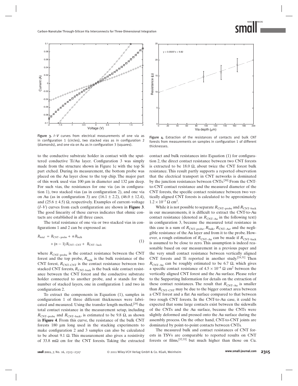
Figure 3 . I – V curves from electrical measurements of one via as
in confi guration 1 (circles), two stacked vias as in confi guration 2
(diamonds), and one via on Au as in confi guration 3 (squares).
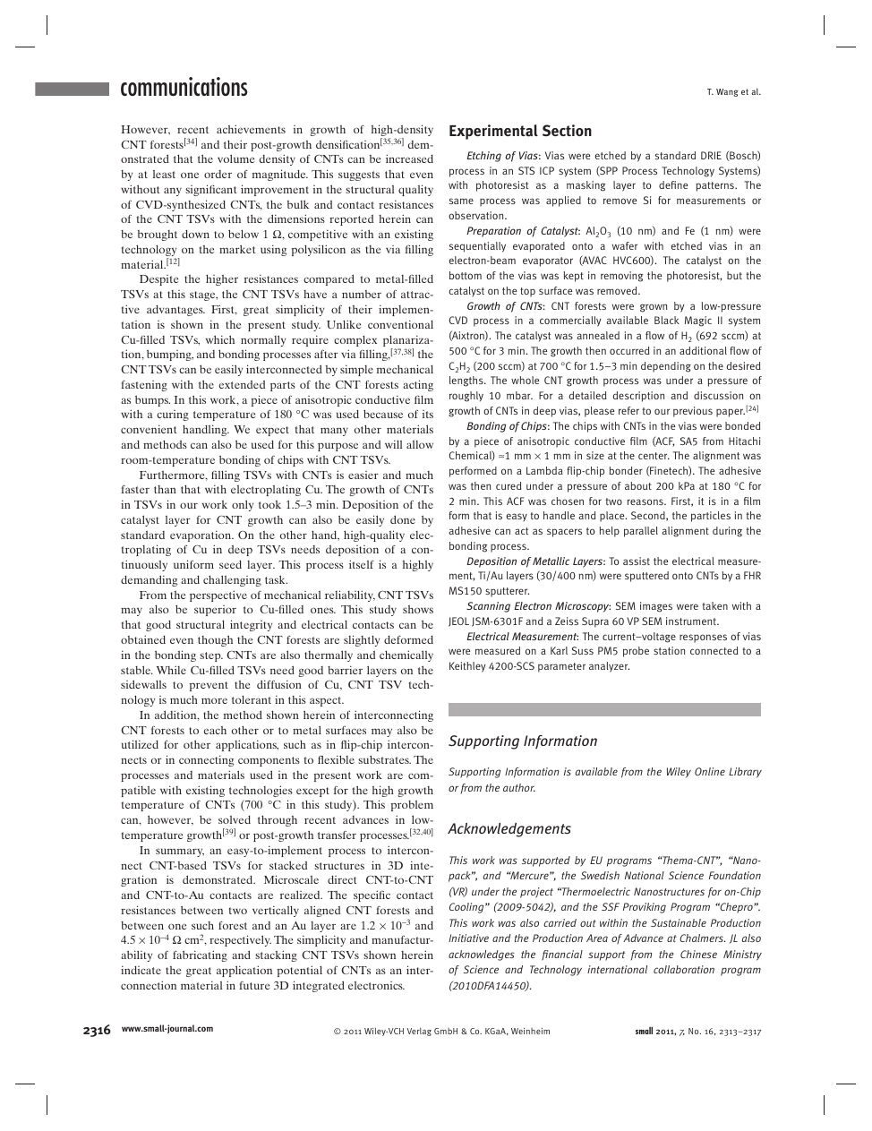
Figure 4 . Extraction of the resistances of contacts and bulk CNT
forests from measurements on samples in confi guration 1 of different
thicknesses.
to the conductive substrate holder in contact with the sput-
tered conductive Ti/Au layer. Confi guration 3 was simply
made from the structure shown in Figure 1 c with the top Si
part etched. During its measurement, the bottom probe was
placed on the Au layer close to the top chip. The major part
of this work used vias 100 μ
m deep.
For such vias, the resistances for one via (as in confi gura-
tion 1), two stacked vias (as in confi guration 2), and one via
on Au (as in confi guration 3) are (16.1 ± 2.2), (46.0 ± 12.4),
and (25.6 ± 4.5) Ω
, respectively. Examples of current–voltage
( I – V ) curves from each confi guration are shown in Figure 3 .
The good linearity of these curves indicates that ohmic con-
tacts are established in all three cases.
m in diameter and 132 μ
The total resistance of one via or two stacked vias in con-
fi gurations 1 and 2 can be expressed as:
Rtotal = RCNT−probe + nRbulk
+ (n − 1)RCNT−CNT + RCNT−back
(1)
where R CNT–probe is the contact resistance between the CNT
forest and the top probe, R bulk is the bulk resistance of the
CNT forest, R CNT–CNT is the contact resistance between two
stacked CNT forests, R CNT–back is the back side contact resist-
ance between the CNT forest and the conductive substrate
holder connected to another probe, and n stands for the
number of stacked layers, one in confi guration 1 and two in
confi guration 2.
To extract the components in Equation (1) , samples in
confi guration 1 of three different thicknesses were fabri-
cated and measured. Using the transfer length method, [ 29 ] the
total contact resistance in the measurement setup, including
R CNT–probe and R CNT–back , is estimated to be 9.8 Ω
, as shown
in Figure 4 . From this curve, the resistance of the bulk CNT
forests 180 μ
m long used in the stacking experiments to
make confi guration 2 and 3 samples can also be calculated
to be about 9.1 Ω
. This measurement also gives a resistivity
of 33.8 m Ω
cm for the CNT forests. Taking the extracted
contact and bulk resistances into Equation (1) for confi gura-
tion 2, the direct contact resistance between two CNT forests
is extracted to be 18.0 Ω
, about twice the CNT forest bulk
resistance. This result partly supports a reported observation
that the electrical transport in CNT networks is dominated
by the junction resistances between CNTs. [ 30 ] From the CNT-
to-CNT contact resistance and the measured diameter of the
CNT forests, the specifi c contact resistance between two ver-
tically aligned CNT forests is calculated to be approximately
1.2 × 10 − 3 Ω
cm 2 .
While it is not possible to separate R CNT–probe and R CNT–back
in our measurements, it is diffi cult to extract the CNT-to-Au
contact resistance (denoted as R CNT–Au in the following text)
in confi guration 3, because the measured total resistance in
this case is a sum of R CNT–probe , R bulk , R CNT–Au , and the negli-
gible resistance of the Au layer and from it to the probe. How-
ever, a rough estimation of R CNT–Au can be made if R CNT–back
is assumed to be close to zero. This assumption is indeed rea-
sonable based on our measurement in a previous paper and
the very small contact resistance between vertically aligned
CNT forests and Ti reported in another study. [ 24 , 31 ] Then
R CNT–Au can be roughly estimated to be 6.7 Ω
, which gives
a specifi c contact resistance of 4.5 × 10 − 4 Ω
cm 2 between the
vertically aligned CNT forest and the Au surface. Please refer
to the Supporting Information for details on the extraction of
these contact resistances. The result that R CNT–Au is smaller
than R CNT–CNT may be due to the bigger contact area between
a CNT forest and a fl at Au surface compared to that between
two rough CNT forests. In the CNT-to-Au case, it could be
expected that some large contacts exist between the sidewalls
of the CNTs and the Au surface, because the CNTs were
slightly deformed and pressed onto the Au surface during the
assembly process. On the other hand, CNT-to-CNT joints are
dominated by point-to-point contacts between CNTs.
The measured bulk and contact resistances of CNT for-
ests in TSVs are comparable to reported results on CNT
forests or fi lms, [ 32 , 33 ] but much higher than those on Cu.
small 2011, 7, No. 16, 2313–2317
© 2011 Wiley-VCH Verlag GmbH & Co. KGaA, Weinheim
www.small-journal.com
2315
�
communications
However, recent achievements in growth of high-density
CNT forests [ 34 ] and their post-growth densifi cation [ 35 , 36 ] dem-
onstrated that the volume density of CNTs can be increased
by at least one order of magnitude. This suggests that even
without any signifi cant improvement in the structural quality
of CVD-synthesized CNTs, the bulk and contact resistances
of the CNT TSVs with the dimensions reported herein can
be brought down to below 1 Ω
, competitive with an existing
technology on the market using polysilicon as the via fi lling
material. [ 12 ]
Despite the higher resistances compared to metal-fi lled
TSVs at this stage, the CNT TSVs have a number of attrac-
tive advantages. First, great simplicity of their implemen-
tation is shown in the present study. Unlike conventional
Cu-fi lled TSVs, which normally require complex planariza-
tion, bumping, and bonding processes after via fi lling, [ 37 , 38 ] the
CNT TSVs can be easily interconnected by simple mechanical
fastening with the extended parts of the CNT forests acting
as bumps. In this work, a piece of anisotropic conductive fi lm
with a curing temperature of 180 ° C was used because of its
convenient handling. We expect that many other materials
and methods can also be used for this purpose and will allow
room-temperature bonding of chips with CNT TSVs.
Furthermore, fi lling TSVs with CNTs is easier and much
faster than that with electroplating Cu. The growth of CNTs
in TSVs in our work only took 1.5–3 min. Deposition of the
catalyst layer for CNT growth can also be easily done by
standard evaporation. On the other hand, high-quality elec-
troplating of Cu in deep TSVs needs deposition of a con-
tinuously uniform seed layer. This process itself is a highly
demanding and challenging task.
From the perspective of mechanical reliability, CNT TSVs
may also be superior to Cu-fi lled ones. This study shows
that good structural integrity and electrical contacts can be
obtained even though the CNT forests are slightly deformed
in the bonding step. CNTs are also thermally and chemically
stable. While Cu-fi lled TSVs need good barrier layers on the
sidewalls to prevent the diffusion of Cu, CNT TSV tech-
nology is much more tolerant in this aspect.
In addition, the method shown herein of interconnecting
CNT forests to each other or to metal surfaces may also be
utilized for other applications, such as in fl ip-chip intercon-
nects or in connecting components to fl exible substrates. The
processes and materials used in the present work are com-
patible with existing technologies except for the high growth
temperature of CNTs (700 ° C in this study). This problem
can, however, be solved through recent advances in low-
temperature growth [ 39 ] or post-growth transfer processes. [ 32 , 40 ]
In summary, an easy-to-implement process to intercon-
nect CNT-based TSVs for stacked structures in 3D inte-
gration is demonstrated. Microscale direct CNT-to-CNT
and CNT-to-Au contacts are realized. The specifi c contact
resistances between two vertically aligned CNT forests and
between one such forest and an Au layer are 1.2 × 10 − 3 and
4.5 × 10 − 4 Ω
cm 2 , respectively. The simplicity and manufactur-
ability of fabricating and stacking CNT TSVs shown herein
indicate the great application potential of CNTs as an inter-
connection material in future 3D integrated electronics.
T. Wang et al.
Experimental Section
Etching of Vias : Vias were etched by a standard DRIE (Bosch)
process in an STS ICP system (SPP Process Technology Systems)
with photoresist as a masking layer to defi ne patterns. The
same process was applied to remove Si for measurements or
observation.
Preparation of Catalyst : Al 2 O 3 (10 nm) and Fe (1 nm) were
sequentially evaporated onto a wafer with etched vias in an
electron-beam evaporator (AVAC HVC600). The catalyst on the
bottom of the vias was kept in removing the photoresist, but the
catalyst on the top surface was removed.
Growth of CNTs : CNT forests were grown by a low-pressure
CVD process in a commercially available Black Magic II system
(Aixtron). The catalyst was annealed in a fl ow of H 2 (692 sccm) at
500 ° C for 3 min. The growth then occurred in an additional fl ow of
C 2 H 2 (200 sccm) at 700 ° C for 1.5–3 min depending on the desired
lengths. The whole CNT growth process was under a pressure of
roughly 10 mbar. For a detailed description and discussion on
growth of CNTs in deep vias, please refer to our previous paper. [ 24 ]
Bonding of Chips : The chips with CNTs in the vias were bonded
by a piece of anisotropic conductive fi lm (ACF, SA5 from Hitachi
Chemical) ≈ 1 mm × 1 mm in size at the center. The alignment was
performed on a Lambda fl ip-chip bonder (Finetech). The adhesive
was then cured under a pressure of about 200 kPa at 180 ° C for
2 min. This ACF was chosen for two reasons. First, it is in a fi lm
form that is easy to handle and place. Second, the particles in the
adhesive can act as spacers to help parallel alignment during the
bonding process.
Deposition of Metallic Layers : To assist the electrical measure-
ment, Ti/Au layers (30/400 nm) were sputtered onto CNTs by a FHR
MS150 sputterer.
Scanning Electron Microscopy : SEM images were taken with a
JEOL JSM-6301F and a Zeiss Supra 60 VP SEM instrument.
Electrical Measurement : The current–voltage responses of vias
were measured on a Karl Suss PM5 probe station connected to a
Keithley 4200-SCS parameter analyzer.
Supporting Information
Supporting Information is available from the Wiley Online Library
or from the author.
Acknowledgements
This work was supported by EU programs “Thema-CNT”, “Nano-
pack”, and “Mercure”, the Swedish National Science Foundation
(VR) under the project “Thermoelectric Nanostructures for on-Chip
Cooling” (2009-5042), and the SSF Proviking Program “Chepro”.
This work was also carried out within the Sustainable Production
Initiative and the Production Area of Advance at Chalmers. JL also
acknowledges the fi nancial support from the Chinese Ministry
of Science and Technology international collaboration program
(2010DFA14450).
2316 www.small-journal.com
© 2011 Wiley-VCH Verlag GmbH & Co. KGaA, Weinheim
small 2011, 7, No. 16, 2313–2317
�
Carbon-Nanotube Through-Silicon Via Interconnects for Three-Dimensional Integration
[ 1 ] R. Tummala , IEEE Spectrum 2006 , 43 , 44 .
[ 2 ] P. Emma , E. Kursun , IBM J. Res. Dev. 2008 , 52 , 541 .
[ 3 ] N. Tanaka , Y. Yoshimira , T. Naito , C. Miyazaki , Y. Nemoto ,
M. Nakanishi , T. Akazawa , in Proceedings of the 55th Electronic
Components and Technology Conference, Lake Buena Vista, FL,
USA , May 2005 .
[ 4 ] M. Motoyoshi , M. Koyanagi , J. Instrum. 2009 , 4 , P03009 .
[ 5 ] Y. Fu , T. Wang , O. Jonsson , J. Liu , J. Micromech. Microeng. 2010 ,
20 , 025027 .
[ 6 ] L. Shen , W. Chien , J. Jaung , Y. Hung , W. Lo , C. Hsu , Y. Lee , H. Cheng ,
C. Lin , in Proceedings of the 58th Electronic Components and
Technology Conference, Lake Buena Vista, FL, USA , May 2008 .
[ 7 ] M. Newman , S. Muthukumar , M. Schuelein , T. Dambrauskas ,
P. Dunaway , J. Jordan , S. Kulkarni , C. Linde , T. Opheim , R. Stingel ,
W. Worwag , L. Topic , J. Swan , in Proceedings of the 56th Elec-
tronic Components and Technology Conference, San Diego, CA,
USA , May 2006 .
[ 20 ] Y. Awano , S. Sato , M. Nihei , T. Sakai , Y. Ohno , T. Mizutani , Proc.
IEEE 2010 , 98 , 2015 .
[ 21 ] B. C. Kim , S. Kannan , A. Gupta , F. Mohammed , B. Ahn , J. Nano-
technol. Eng. Med. 2010 , 1 , 021012 .
[ 22 ] C. Xu , H. Li , R. Suaya , K. Banerjee , IEEE Trans. Electron Devices
2010 , 57 , 3405 .
[ 23 ] T. Xu , Z. Wang , J. Miao , X. Chen , C. Tan , Appl. Phys. Lett. 2007 , 91 ,
042108 .
[ 24 ] T. Wang , K. Jeppson , N. Olofsson , E. Campbell , J. Liu , Nanotech-
nology 2009 , 20 , 485203 .
[ 25 ] K. Yung , J. Wei , B. Tay , Diamond Relat. Mater. 2009 , 18 , 1109 .
[ 26 ] H. Ko , Z. Zhang , J. C. Ho , K. Takei , R. Kapadia , Y. Chueh , W. Cao ,
B. A. Cruden , A. Javey , Small 2010 , 6 , 22 .
[ 27 ] A. Cao , P. L. Dickrell , W. G. Sawyer , M. N. Ghasemi-Nejhad ,
P. M. Ajayan , Science 2005 , 310 , 1307 .
[ 28 ] L. Qu , L. Dai , M. Stone , Z. Xia , Z. L. Wang , Science 2008 , 322 ,
238 .
[ 8 ] N. Ranganathan , K. Prasad , N. Balasubramanian , K. Pey , J. Micro-
[ 29 ] D. K. Schroder , Semiconductor Material and Device Characteriza-
mech. Microeng. 2008 , 18 , 075018 .
tion , Wiley , New York , 1998 , p. 156 .
[ 9 ] K. H. Lu , S. Ryu , Q. Zhao , X. Zhang , J. Im , R. Huang , P. S. Ho , in
Proceedings of the 60th Electronic Components and Technology
Conference, Las Vegas, NV, USA , June 2010 .
[ 10 ] S. Ramaswami , J. Dukovic , B. Eaton , S. Pamarthy , A. Bhatnagar ,
Z. Cao , K. Sapre , Y. Wang , A. Kumar , IEEE Trans. Device Mater.
Reliab. 2009 , 9 , 524 .
[ 30 ] P. N. Nirmalraj , P. E. Lyons , S. De , J. N. Coleman , J. J. Boland , Nano
Lett. 2009 , 9 , 3890 .
[ 31 ] S. C. Lim , J. H. Jang , D. J. Bae , G. H. Han , S. Lee , I. Yeo , Y. H. Lee ,
Appl. Phys. Lett. 2009 , 95 , 264103 .
[ 32 ] Y. Fu , Y. Qin , T. Wang , S. Chen , J. Liu , Adv. Mater. 2010 , 22 ,
5039 .
[ 11 ] H. Kikuchi , Y. Yamada , A. Ali , J. Liang , T. Fukushima , T. Tanaka ,
[ 33 ] H. Xu , L. Chen , L. Hu , N. Zhitenev , Appl. Phys. Lett. 2010 , 97 ,
M. Koyanagi , Jpn. J. Appl. Phys. 2008 , 47 , 2801 .
143116 .
[ 12 ] M. Rimskog , in Proceedings of the IEEE/CPMT International Elec-
tronics Manufacturing Technology Symposium, San Jose, CA,
USA , Oct 2007 .
[ 13 ] M. Falvo , G. Clary , R. Taylor II , V. Chi , F. Brooks , Jr. , S. Washburn ,
R. Superfi ne , Nature 1997 , 389 , 582 .
[ 14 ] H. Jiang , B. Liu , Y. Huang , K. C. Hwang , J. Eng. Mater. Technol.
2004 , 126 , 265 .
[ 15 ] B. Wei , R. Vajtai , P. Ajayan , Appl. Phys. Lett. 2001 , 79 , 1172 .
[ 16 ] P. G. Collins , M. Hersam , M. Arnold , R. Martel , P. Avouris , Phys.
Rev. Lett. 2001 , 86 , 3128 .
[ 17 ] T. Ragab , C. Basaran , J. Appl. Phys. 2009 , 106 , 063705 .
[ 18 ] J. Hone , M. Whitney , C. Piskoti , A. Zettl , Phys. Rev. B 1999 , 59 ,
R2514 .
[ 19 ] D. Bom , R. Andrews , D. Jacques , J. Anthony , B. Chen , M. S. Meier ,
J. P. Selegue , Nano Lett. 2002 , 2 , 615 .
[ 34 ] S. Esconjauregui , M. Fouquet , B. Bayer , C. Ducati , R. Smajda ,
S. Hofmann , J. Robertson , ACS Nano 2010 , 4 , 7431 .
[ 35 ] D. Futaba , K. Hata , T. Yamada , T. Hiraoka , Y. Hayamizu , Y. Kakudate ,
O. Tanaike , H. Hatori , M. Yumura , S. Iijima , Nat. Mater. 2006 , 5 ,
987 .
[ 36 ] T. Wang , K. Jeppson , J. Liu , Carbon 2010 , 48 , 3795 .
[ 37 ] J.-Q. Lu , Proc. IEEE 2009 , 97 , 18 – 30 .
[ 38 ] M. Koyanagi , T. Fukushima , T. Tanaka , Proc. IEEE 2009 , 97 , 49 .
[ 39 ] M. Cantoro , S. Hofmann , S. Pisana , V. Scardaci , A. Parvez ,
C. Ducati , A. C. Ferrari , A. M. Blackburn , K. Wang , J. Robertson ,
Nano Lett. 2006 , 6 , 1107 .
[ 40 ] T. Wang , B. Carlberg , M. Jönsson , G. Jeong , E. Campbell , J. Liu ,
Appl. Phys. Lett. 2007 , 91 , 093123 .
Received: March 31, 2011
Published online: June 21, 2011
small 2011, 7, No. 16, 2313–2317
© 2011 Wiley-VCH Verlag GmbH & Co. KGaA, Weinheim
www.small-journal.com
2317
�


 2023年江西萍乡中考道德与法治真题及答案.doc
 2012年重庆南川中考生物真题及答案.doc
 2013年江西师范大学地理学综合及文艺理论基础考研真题.doc
 2020年四川甘孜小升初语文真题及答案I卷.doc
 2020年注册岩土工程师专业基础考试真题及答案.doc
 2023-2024学年福建省厦门市九年级上学期数学月考试题及答案.doc
 2021-2022学年辽宁省沈阳市大东区九年级上学期语文期末试题及答案.doc
 2022-2023学年北京东城区初三第一学期物理期末试卷及答案.doc
 2018上半年江西教师资格初中地理学科知识与教学能力真题及答案.doc
 2012年河北国家公务员申论考试真题及答案-省级.doc
 2020-2021学年江苏省扬州市江都区邵樊片九年级上学期数学第一次质量检测试题及答案.doc
 2022下半年黑龙江教师资格证中学综合素质真题及答案.doc