Design of 56 Gb/s PAM4 Wire-line Receiver With Ring VCO Based CDR in a 65 nm
CMOS Technology
Fangxu Lv1,2, Jianye Wang1*, Dengjie Wang2, Yongcong Liu1, Ziqiang Wang2*
1
Air and Missile Defense College, Air Force Engineering University, xi’an 710051, China
2
The Institute of Microelectronics, Tsinghua University, Beijing 100084, China
E-mail: wangziq@mail.tsinghua.edu.cn; lvfangxu1988@163.com.cn;
Abstract
This paper presents a 56 Gb/s 4-level pulse amplitude
modulation (PAM4) wire-line receiver, which employs a
quarter rate architecture. By employing a ring voltage control
oscillator (VCO) based clock and data recovery (CDR) with
separate proportional path, the complexity, power consumption
and area can all be reduced. To reduce the noise of the detector
and improve the stability of the CDR, both the major and minor
transitions with the central crossover point are utilized to
extract the phase error. The receiver is designed in a 65nm
CMOS technology and supplied with 1.2V. The simulation
results show that the proposed PAM4 receiver can work at 56
Gb/s with 76 mW consumption.
1. Introduction
The rapid development of many applications, such as internet
of things (IoT), big data and cloud computing leads to
bandwidth exponential growth demand on computer systems,
communication networks, and the bulk of consumer electronics
[1]. This increasing bandwidth demand has pushed serial-link
towards data-rates of 40 Gb/s or beyond [2-3]. Nevertheless, as
data rate increases, the bandwidth constraints imposed by the
channel, package, and ESD become more severe, which
severely limits the development of the non-return-zero (NRZ)
signaling. The 4-level pulse amplitude modulation (PAM4) is
drawing widely attentions due to its two-fold bandwidth
efficiency than NRZ signaling[4].
However, the design of the PAM4 receiver is more difficult
than that of the NRZ receiver, especially when data rate reaches
56 Gb/s. Clock and data recovery (CDR) is the most
challenging part of the PAM4 receiver design, since it has to
deal with multi-level. All of the three slicer’s outputs have side
crossover point in transition, which inevitably introduces extra
noise of phase detector (PD) and leads to the CDR unstable. In
[4], the CDR only uses the middle slicer output’s signal to
extract the phase error, because it has more central crossover
point transitions than others. However, the middle slicer output
also has sidle crossover point transition. In this paper, by
employing a transition filter, all useful transitions generated by
the three slicers with central crossover point are utilized to
extract the phase error. In addition, to reduce the complexity,
power consumption and area, a ring VCO based CDR with a
separated proportional path is applied to provide local clock.
2. Architecture
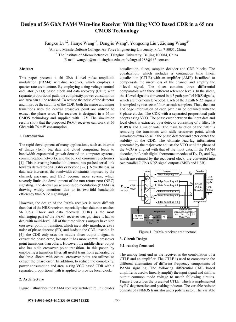
Figure 1 illustrates the PAM4 receiver architecture. It includes
time
includes a continuous
equalization, slicer, sampler, decoder and CDR blocks. The
equalization, which
linear
equalization (CTLE) with an amplifier (AMP), is utilized to
compensate the insert loss of the channel and amplify the
4-level signal. The slicer contains
three differential
comparators with three different reference levels. In the slicer,
the 4-level signal is converted into 3 path parallel NRZ signals,
which are thermometer-coded. Each of the 3 path NRZ signals
is sampled by two sets of four cascade samplers. Thus, the data
and edge information of each path can be obtained with the
8-phase clocks. The CDR with a separated proportional path
adopts a ring VCO. The phase error between the input data and
local clock is extracted by a detector consisting of a filter, 16
BBPDs and a major vote. The main function of the filter is
removing the transitions with sidle crossover point, which
introduces extra noise in the phase detector and deteriorates the
stability of the CDR. The ultimate lead-lag information
generated by the major vote adjusts the VCO until the phase of
the VCO is aligned with that of the input data. In the PAM4
decoder, the 3 path digital thermometer codes of DA, DB and DC,
which are retimed by the recovered clock, are converted into
two parallel 7 Gb/s NRZ signal outputs (MSB and LSB).
Figure 1. PAM4 receiver architecture.
3. Circuit Design
3.1. Analog front end
The analog front end in the receiver is the combination of a
CTLE and an amplifier. The CTLE is used to compensate the
different attenuation of different frequency components of
PAM4 signaling. The following differential CML based
amplifier is used to linearly amplify the input signal and shift its
output common mode voltage to match following circuits.
Figure 2 describes the presented CTLE, which is implemented
by RC degeneration and peaking inductor. The variable resistor
consists of a NMOS transistor and a poly resistor. The variable
PAM4 DigitalDecoderTransition filterMSB7 Gb/s4DADBDCCPRing VCO7 GHzProportional Integral 8 phase Clock Gen.8X4INDLSB7 Gb/s4CDRSlicerCTLE/AMPVASamplerVBVCDecoderData Sampling X 4Edge Sampling X 4Data Sampling X 4Edge Sampling X 4Edge Sampling X 4BBPDX 4BBPDX 4Data Sampling X 444BBPDX 4BBPDX 4Major Voter56 Gb/s978-1-5090-6625-4/17/$31.00 ©2017 IEEE 553 �
capacitance consists of two NMOS transistors. The boost gain
of the CTLE can be continuously changed through adjusting
the gate voltage of the transistors at low frequency. In addition,
the peaking inductor is utilized to extend the bandwidth and the
boost gain of the CTLE without increasing power consumption.
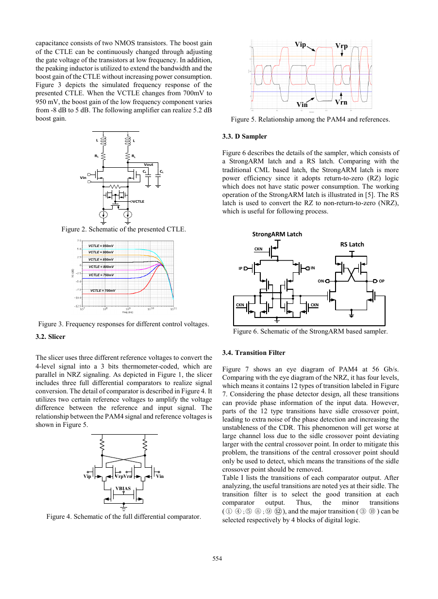
Figure 3 depicts the simulated frequency response of the
presented CTLE. When the VCTLE changes from 700mV to
950 mV, the boost gain of the low frequency component varies
from -8 dB to 5 dB. The following amplifier can realize 5.2 dB
boost gain.
Figure 2. Schematic of the presented CTLE.
Figure 3. Frequency responses for different control voltages.
3.2. Slicer
The slicer uses three different reference voltages to convert the
4-level signal into a 3 bits thermometer-coded, which are
parallel in NRZ signaling. As depicted in Figure 1, the slicer
includes three full differential comparators to realize signal
conversion. The detail of comparator is described in Figure 4. It
utilizes two certain reference voltages to amplify the voltage
difference between the reference and input signal. The
relationship between the PAM4 signal and reference voltages is
shown in Figure 5.
Figure 4. Schematic of the full differential comparator.
Figure 5. Relationship among the PAM4 and references.
3.3. D Sampler
Figure 6 describes the details of the sampler, which consists of
a StrongARM latch and a RS latch. Comparing with the
traditional CML based latch, the StrongARM latch is more
power efficiency since it adopts return-to-zero (RZ) logic
which does not have static power consumption. The working
operation of the StrongARM latch is illustrated in [5]. The RS
latch is used to convert the RZ to non-return-to-zero (NRZ),
which is useful for following process.
Figure 6. Schematic of the StrongARM based sampler.
3.4. Transition Filter
Figure 7 shows an eye diagram of PAM4 at 56 Gb/s.
Comparing with the eye diagram of the NRZ, it has four levels,
which means it contains 12 types of transition labeled in Figure
7. Considering the phase detector design, all these transitions
can provide phase information of the input data. However,
parts of the 12 type transitions have sidle crossover point,
leading to extra noise of the phase detection and increasing the
unstableness of the CDR. This phenomenon will get worse at
large channel loss due to the sidle crossover point deviating
larger with the central crossover point. In order to mitigate this
problem, the transitions of the central crossover point should
only be used to detect, which means the transitions of the sidle
crossover point should be removed.
Table I lists the transitions of each comparator output. After
analyzing, the useful transitions are noted yes at their sidle. The
transition filter is to select the good transition at each
transitions
comparator
(
) can be
selected respectively by 4 blocks of digital logic.
the minor
), and the major transition (
;
output.
Thus,
;
VinVoutRLCLRLLLCLVCTLEVCTLE = 700mVVCTLE = 800mVVCTLE = 850mVVCTLE = 950mVVCTLE = 900mVVCTLE = 750mVVipVinVrnVrpVBIASVipVinVrpVrnCKNONOPIPINRS LatchStrongARM LatchCKNCKN①④⑤⑧⑨⑫③⑩554 �
frequency step of the separated proportional path, Icp is the
charge pump current, Kvco is the turning gain of the VCO in
Hz/V, and
is the baud rate. In order to guarantee the
stability, the
should be designed largely [7]. In addition,
the jitter tolerance should also be analyzed and designed. Paper
[6], shows the analytic expression for the maximum input phase
jitter
that causes the onset of the slew rate limiting
(2)
,
is the input sinusoidal jitter frequency. The
Where
tolerable sinusoidal jitter amplitude should be greater than
0.1UI at
for most standards. Numerical
simulation result indicates that large
can get large jitter
tolerance but large
also leads to large self-generated
hunting jitter, which will deteriorate the recovered clock
performance.
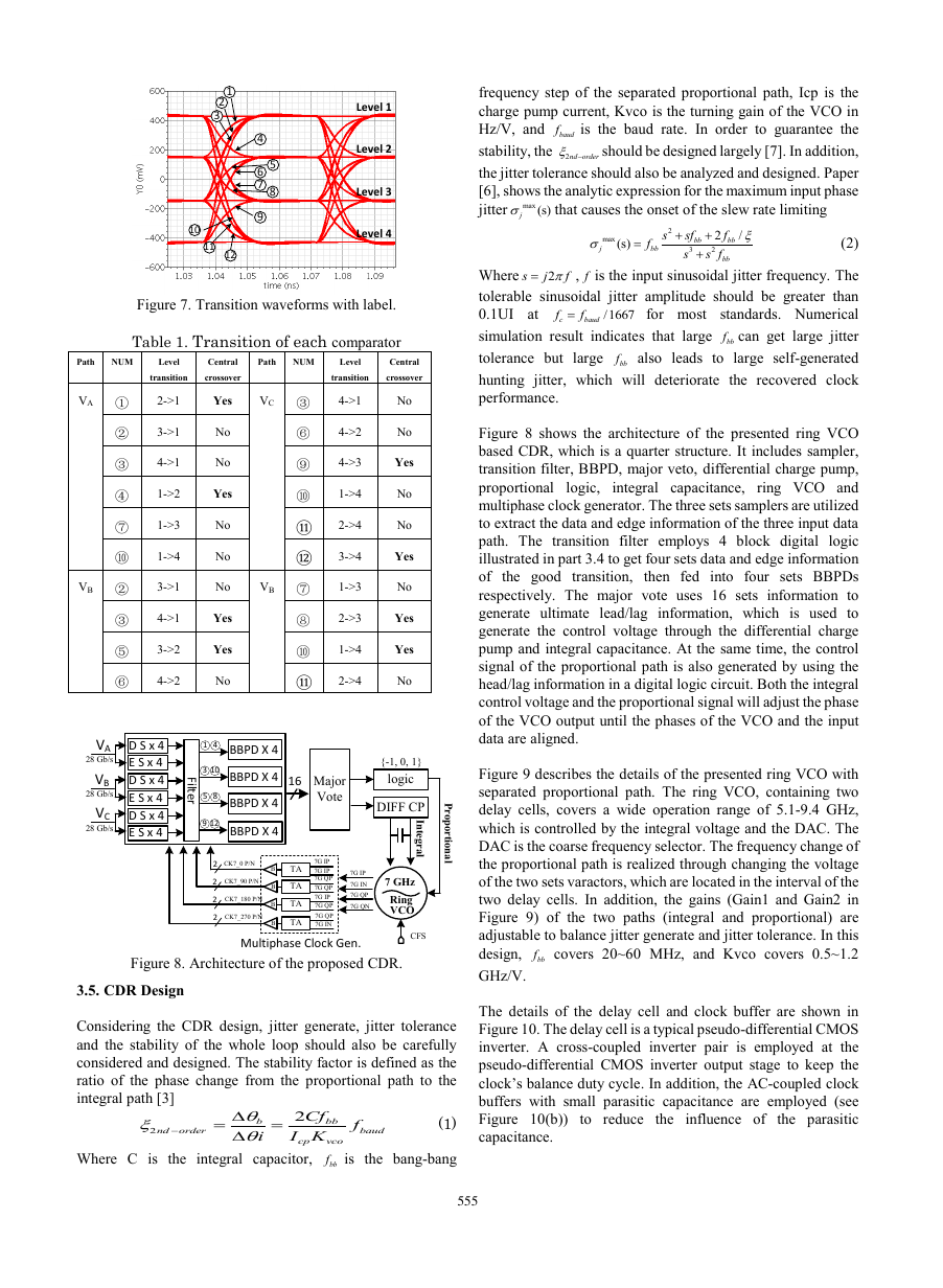
Figure 8 shows the architecture of the presented ring VCO
based CDR, which is a quarter structure. It includes sampler,
transition filter, BBPD, major veto, differential charge pump,
proportional logic, integral capacitance, ring VCO and
multiphase clock generator. The three sets samplers are utilized
to extract the data and edge information of the three input data
path. The transition filter employs 4 block digital logic
illustrated in part 3.4 to get four sets data and edge information
of the good transition, then fed into four sets BBPDs
respectively. The major vote uses 16 sets information to
generate ultimate lead/lag information, which is used to
generate the control voltage through the differential charge
pump and integral capacitance. At the same time, the control
signal of the proportional path is also generated by using the
head/lag information in a digital logic circuit. Both the integral
control voltage and the proportional signal will adjust the phase
of the VCO output until the phases of the VCO and the input
data are aligned.
Figure 9 describes the details of the presented ring VCO with
separated proportional path. The ring VCO, containing two
delay cells, covers a wide operation range of 5.1-9.4 GHz,
which is controlled by the integral voltage and the DAC. The
DAC is the coarse frequency selector. The frequency change of
the proportional path is realized through changing the voltage
of the two sets varactors, which are located in the interval of the
two delay cells. In addition, the gains (Gain1 and Gain2 in
Figure 9) of the two paths (integral and proportional) are
adjustable to balance jitter generate and jitter tolerance. In this
design,
covers 20~60 MHz, and Kvco covers 0.5~1.2
GHz/V.
The details of the delay cell and clock buffer are shown in
Figure 10. The delay cell is a typical pseudo-differential CMOS
inverter. A cross-coupled inverter pair is employed at the
pseudo-differential CMOS inverter output stage to keep the
clock’s balance duty cycle. In addition, the AC-coupled clock
buffers with small parasitic capacitance are employed (see
Figure 10(b)) to reduce the influence of the parasitic
capacitance.
Figure 7. Transition waveforms with label.
Table 1. Transition of each comparator
Path
NUM
Level
Central
Path
NUM
Level
Central
transition
crossover
transition
crossover
2->1
Yes
VC
3->1
No
4->1
No
1->2
Yes
1->3
No
1->4
No
3->1
No
VB
4->1
Yes
3->2
Yes
4->2
No
4->1
4->2
No
No
4->3
Yes
1->4
2->4
No
No
3->4
Yes
1->3
No
2->3
Yes
1->4
Yes
2->4
No
VA
VB
Figure 8. Architecture of the proposed CDR.
3.5. CDR Design
Considering the CDR design, jitter generate, jitter tolerance
and the stability of the whole loop should also be carefully
considered and designed. The stability factor is defined as the
ratio of the phase change from the proportional path to the
integral path [3]
(1)
Where C is the integral capacitor,
is the bang-bang
Level 1123456879101112Level 2Level 3Level 4①③②⑥③⑨④⑩⑦⑪⑩⑫②⑦③⑧⑤⑩⑥⑪MajorVoteBBPD X 4 DIFF CPlogicIntegral TA7G IP7G IN7G QP7G QN7G IPTATATA7G QP7G INCK7_0 P/NCK7_90 P/NCK7_180 P/NCK7_270 P/N{-1, 0, 1}162222E S x 428 Gb/s VB7 GHz 7G IP7G IP7G QP7G QP7G QPBBBBMultiphase Clock Gen.D S x 4E S x 4D S x 4E S x 4D S x 4FilterBBPD X 4 BBPD X 4 BBPD X 4 1431058912VAVCVCORingCFSProportional 28 Gb/s 28 Gb/s 22bbbndorderbaudcpvcoCffiIKbbfbaudf2ndordermax(s)j2max322/(s)bbbbjbbbbssfffssf2sjff/1667cbaudffbbfbbfbbf555 �
Figure 9. Ring VCO with separated proportional path.
(a) (b)
Figure 10. Details of (a) delay cell, (b) clock buffer
Figure 11. PAM4 receiver layout
4. Experimental results
The PAM4 receiver is design in a 65nm CMOS technology and
its layout is shown in Figure 11. The core circuit occupies area
of 0.375 mm2 and consumes 76 mW under 1.2 V supply. When
the receiver inputs PRBS7 based PAM4 data, parts of
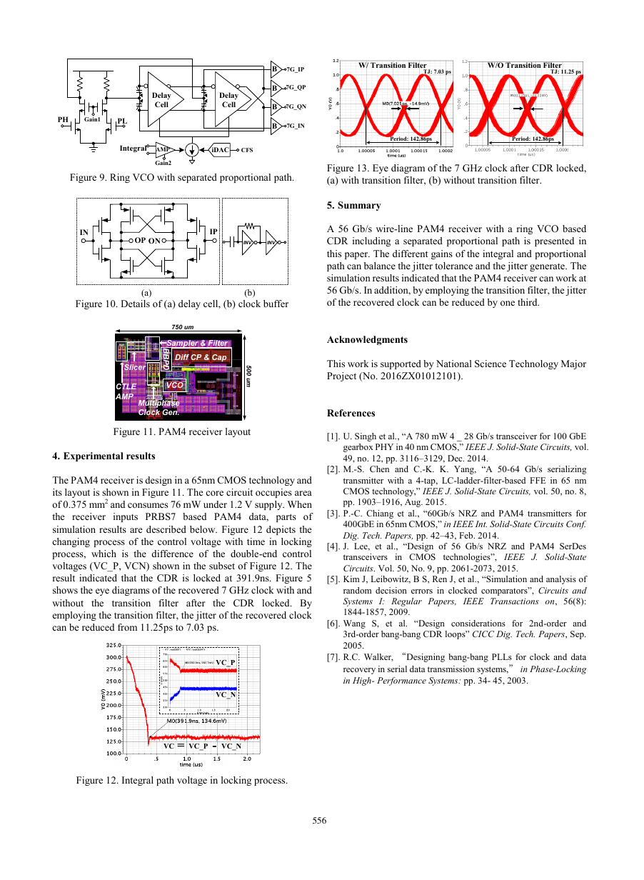
simulation results are described below. Figure 12 depicts the
changing process of the control voltage with time in locking
process, which is the difference of the double-end control
voltages (VC_P, VCN) shown in the subset of Figure 12. The
result indicated that the CDR is locked at 391.9ns. Figure 5
shows the eye diagrams of the recovered 7 GHz clock with and
without the transition filter after the CDR locked. By
employing the transition filter, the jitter of the recovered clock
can be reduced from 11.25ps to 7.03 ps.
Figure 13. Eye diagram of the 7 GHz clock after CDR locked,
(a) with transition filter, (b) without transition filter.
5. Summary
A 56 Gb/s wire-line PAM4 receiver with a ring VCO based
CDR including a separated proportional path is presented in
this paper. The different gains of the integral and proportional
path can balance the jitter tolerance and the jitter generate. The
simulation results indicated that the PAM4 receiver can work at
56 Gb/s. In addition, by employing the transition filter, the jitter
of the recovered clock can be reduced by one third.
Acknowledgments
This work is supported by National Science Technology Major
Project (No. 2016ZX01012101).
References
[1]. U. Singh et al., “A 780 mW 4 _ 28 Gb/s transceiver for 100 GbE
gearbox PHY in 40 nm CMOS,” IEEE J. Solid-State Circuits, vol.
49, no. 12, pp. 3116–3129, Dec. 2014.
[2]. M.-S. Chen and C.-K. K. Yang, “A 50-64 Gb/s serializing
transmitter with a 4-tap, LC-ladder-filter-based FFE in 65 nm
CMOS technology,” IEEE J. Solid-State Circuits, vol. 50, no. 8,
pp. 1903–1916, Aug. 2015.
[3]. P.-C. Chiang et al., “60Gb/s NRZ and PAM4 transmitters for
400GbE in 65nm CMOS,” in IEEE Int. Solid-State Circuits Conf.
Dig. Tech. Papers, pp. 42–43, Feb. 2014.
[4]. J. Lee, et al., “Design of 56 Gb/s NRZ and PAM4 SerDes
transceivers in CMOS technologies”, IEEE J. Solid-State
Circuits. Vol. 50, No. 9, pp. 2061-2073, 2015.
[5]. Kim J, Leibowitz, B S, Ren J, et al., “Simulation and analysis of
random decision errors in clocked comparators”, Circuits and
Systems I: Regular Papers, IEEE Transactions on, 56(8):
1844-1857, 2009.
[6]. Wang S, et al. “Design considerations for 2nd-order and
3rd-order bang-bang CDR loops” CICC Dig. Tech. Papers, Sep.
2005.
[7]. R.C. Walker, “Designing bang-bang PLLs for clock and data
recovery in serial data transmission systems,” in Phase-Locking
in High- Performance Systems: pp. 34- 45, 2003.
Figure 12. Integral path voltage in locking process.
DelayCellDelayCellPLBBBB7G_IPiDACIntegralCFSPHGain17G_IN7G_QP7G_QNAMPGain2INIPOPONINVINV750 umCTLEAMPSampler & FilterSlicerMultiphaseClock Gen.VCOBBPDDiff CP & Cap500 umVC_PVC_NVC_PVC_N-VC=TJ: 11.25 psPeriod: 142.86psPeriod: 142.86psTJ: 7.03 psW/ Transition FilterW/O Transition Filter556 �


 2023年江西萍乡中考道德与法治真题及答案.doc
 2012年重庆南川中考生物真题及答案.doc
 2013年江西师范大学地理学综合及文艺理论基础考研真题.doc
 2020年四川甘孜小升初语文真题及答案I卷.doc
 2020年注册岩土工程师专业基础考试真题及答案.doc
 2023-2024学年福建省厦门市九年级上学期数学月考试题及答案.doc
 2021-2022学年辽宁省沈阳市大东区九年级上学期语文期末试题及答案.doc
 2022-2023学年北京东城区初三第一学期物理期末试卷及答案.doc
 2018上半年江西教师资格初中地理学科知识与教学能力真题及答案.doc
 2012年河北国家公务员申论考试真题及答案-省级.doc
 2020-2021学年江苏省扬州市江都区邵樊片九年级上学期数学第一次质量检测试题及答案.doc
 2022下半年黑龙江教师资格证中学综合素质真题及答案.doc