Designing Control Loops for Linear and Switching Power Supplies: A Tutorial Guide
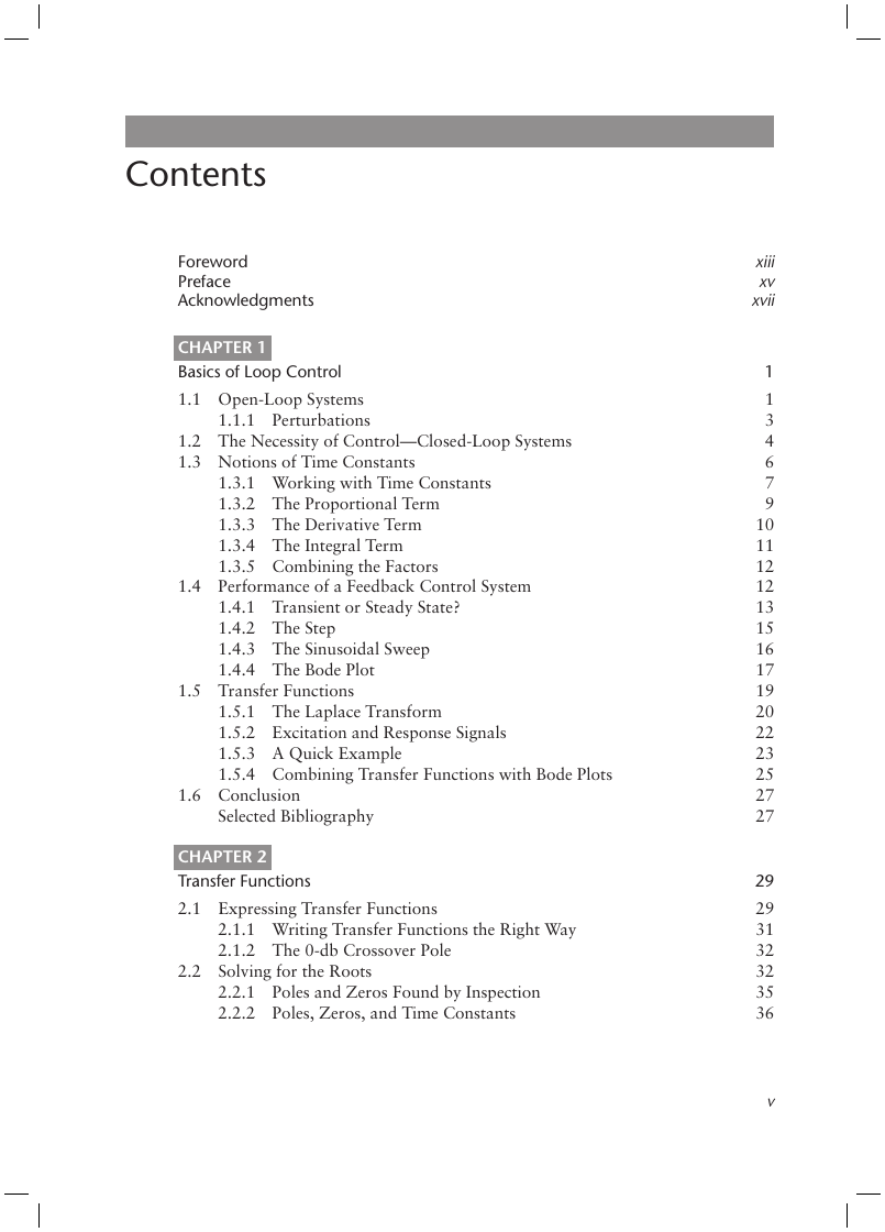
Contents
Foreword
Preface
Acknowledgments
Chapter 1 Basics of Loop Control
1.1 Open-Loop Systems
1.1.1 Perturbations
1.2 The Necessity of Control—Closed-Loop Systems
1.3 Notions of Time Constants
1.3.1 Working with Time Constants
1.3.2 The Proportional Term
1.3.3 The Derivative Term
1.3.4 The Integral Term
1.3.5 Combining the Factors
1.4 Performance of a Feedback Control System
1.4.1 Transient or Steady State?
1.4.2 The Step
1.4.3 The Sinusoidal Sweep
1.4.4 The Bode Plot
1.5 Transfer Functions
1.5.1 The Laplace Transform
1.5.2 Excitation and Response Signals
1.5.3 A Quick Example
1.5.4 Combining Transfer Functions with Bode Plots
1.6 Conclusion
Selected Bibliography
Chapter 2 Transfer Functions
2.1 Expressing Transfer Functions
2.1.1 Writing Transfer Functions the Right Way
2.1.2 The 0-db Crossover Pole
2.2 Solving for the Roots
2.2.1 Poles and Zeros Found by Inspection
2.2.2 Poles, Zeros, and Time Constants
2.3 Transient Response and Roots
2.3.1 When the Roots Are Moving
2.4 S-Plane and Transient Response
2.4.1 Roots Trajectories in the Complex Plane
2.5 Zeros in the Right Half Plane
2.5.1 A Two-Step Conversion Process
2.5.2 The Inductor Current Slew-Rate Is the Limit
2.5.3 An Average Model to Visualize RHP Zero Effects
2.5.4 The Right Half Plane Zero in the Boost Converter
2.6 Conclusion
References
Appendix 2A: Determining a Bridge Input Impedance
Reference
Appendix 2B: Plotting Evans Loci with Mathcad
Appendix 2C: Heaviside Expansion Formulas
Reference
Appendix 2D: Plotting a Right Half Plane Zero with SPICE
Chapter 3 Stability Criteria of a Control System
3.1 Building An Oscillator
3.1.1 Theory at Work
3.2 Stability Criteria
3.2.1 Gain Margin and Conditional Stability
3.2.2 Minimum Versus Nonminimum-Phase Functions
3.2.3 Nyquist Plots
3.2.4 Extracting the Basic Information from the Nyquist Plot
3.2.5 Modulus Margin
3.3 Transient Response, Quality Factor, and Phase Margin
3.3.1 A Second-Order System, the RLC Circuit
3.3.2 Transient Response of a Second-Order System
3.3.4 Opening the Loop to Measure the Phase Margin
3.3.5 The Phase Margin of a Switching Converter
3.3.6 Considering a Delay in the Conversion Process
3.3.7 The Delay in the Laplace Domain
3.3.8 Delay Margin versus Phase Margin
3.4 Selecting the Crossover Frequency
3.4.1 A Simplified Buck Converter
3.4.2 The Output Impedance in Closed-Loop Conditions
3.4.3 The Closed-Loop Output Impedance at Crossover
3.4.4 Scaling the Reference to Obtain the Desired Output
3.4.5 Increasing the Crossover Frequency Further
3.5 Conclusion
References
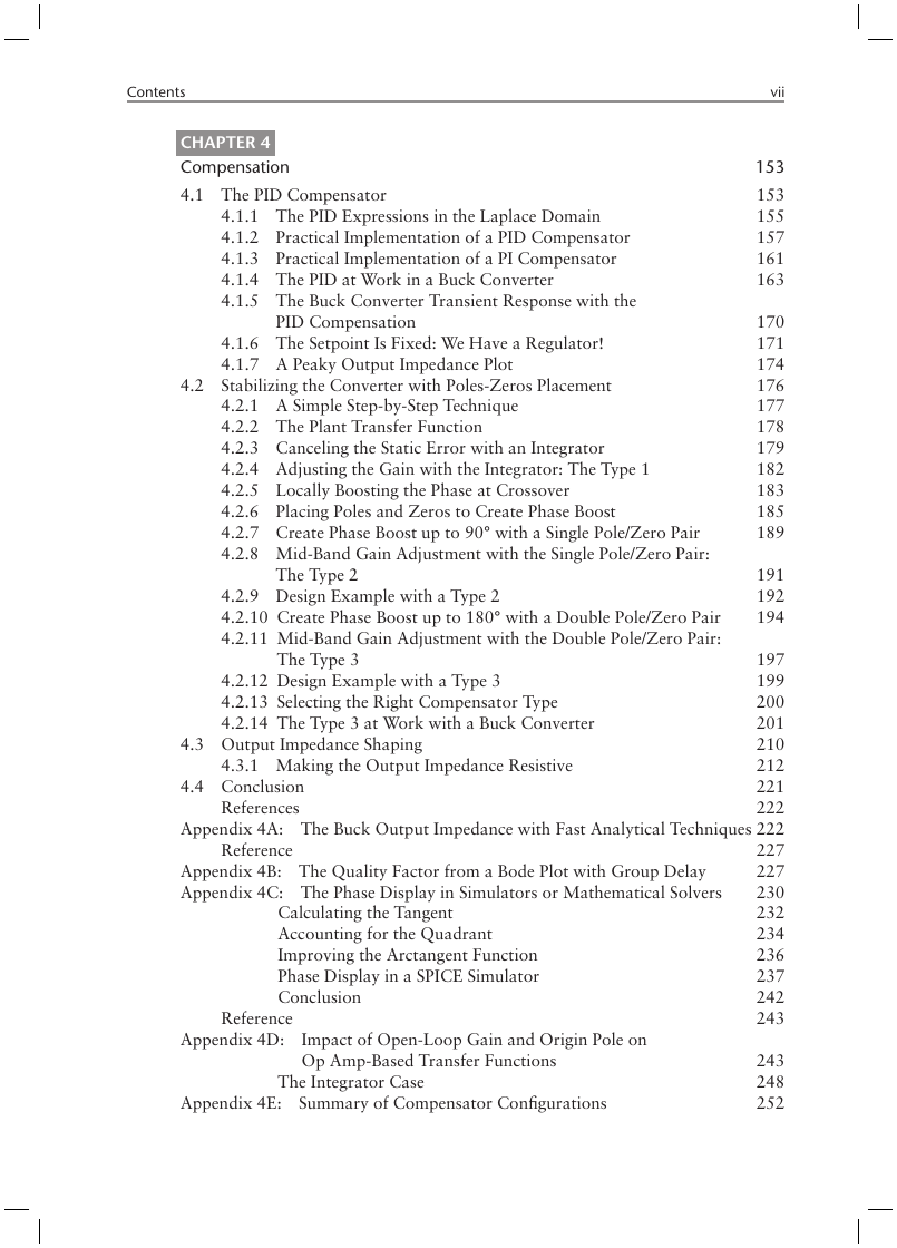
Chapter 4 Compensation
4.1 The PID Compensator
4.1.1 The PID Expressions in the Laplace Domain
4.1.2 Practical Implementation of a PID Compensator
4.1.3 Practical Implementation of a PI Compensator
4.1.4 The PID at Work in a Buck Converter
4.1.5 The Buck Converter Transient Response with the PID Compensation
4.1.6 The Setpoint Is Fixed: We Have a Regulator!
4.1.7 A Peaky Output Impedance Plot
4.2 Stabilizing the Converter with Poles-Zeros Placement
4.2.1 A Simple Step-by-Step Technique
4.2.2 The Plant Transfer Function
4.2.3 Canceling the Static Error with an Integrator
4.2.4 Adjusting the Gain with the Integrator: The Type 1
4.2.5 Locally Boosting the Phase at Crossover
4.2.6 Placing Poles and Zeros to Create Phase Boost
4.2.7 Create Phase Boost up to 90° with a Single Pole/Zero Pair
4.2.8 Mid-Band Gain Adjustment with the Single Pole/Zero Pair: The Type 2
4.2.9 Design Example with a Type 2
4.2.10 Create Phase Boost up to 180° with a Double Pole/Zero Pair
4.2.11 Mid-Band Gain Adjustment with the Double Pole/Zero Pair: The Type 3
4.2.12 Design Example with a Type 3
4.2.13 Selecting the Right Compensator Type
4.2.14 The Type 3 at Work with a Buck Converter
4.3 Output Impedance Shaping
4.3.1 Making the Output Impedance Resistive
4.4 Conclusion
Appendix 4A: The Buck Output Impedance with Fast AnalyticalTechniques
Reference
Appendix 4B: The Quality Factor from a Bode Plot with Group Delay
Appendix 4C: The Phase Display in Simulators or Mathematical Solvers
Reference
Appendix 4D: Impact of Open-Loop Gain and Origin Pole on OpAmp-Based Transfer Functions
Appendix 4E: Summary of Compensator Configurations
Chapter 5 Operational Amplifiers-Based
Compensators
5.1 Type 1: An Origin Pole
5.1.1 A Design Example
5.2 Type 2: An Origin Pole, plus a Pole/Zero Pair
5.2.1 A Design Example
5.3 Type 2a: An Origin Pole plus a Zero
5.3.1 A Design Example
5.4 Type 2b: Some Static Gain plus a Pole
5.4.1 A Design Example
5.5 Type 2: Isolation with an Optocoupler
5.5.1 Optocoupler and Op Amp: the Direct Connection, Common Emitter
5.5.2 A Design Example
5.5.3 Optocoupler and Op Amp: The Direct Connection, Common Collector
5.5.4 Optocoupler and Op Amp: The Direct Connection Common Emitterand UC384X
5.5.5 Optocoupler and Op Amp: Pull Down with Fast Lane
5.5.6 A Design Example
5.5.7 Optocoupler and Op Amp: Pull-Down with Fast Lane, Common Emitter, and UC384X
5.5.8 Optocoupler and Op Amp: Pull Down Without Fast Lane
5.5.9 A Design Example
5.5.10 Optocoupler and Op Amp: A Dual-Loop Approach in CC-CV Applications
5.5.11 A Design Example
5.6 The Type 2: Pole and Zero are Coincident to Createan Isolated Type 1
5.6.1 A Design Example
5.7 The Type 2: A Slightly Different Arrangement
5.8 The Type 3: An Origin Pole, a Pole/Zero Pair
5.8.1 A Design Example
5.9 The Type 3: Isolation with an Optocoupler
5.9.1 Optocoupler and Op Amp: The Direct Connection, Common Collector
5.9.2 A Design Example
5.9.3 Optocoupler and Op Amp: The Direct Connection, Common Emitter
5.9.4 Optocoupler and Op Amp: The Direct Connection, Common Emitter,and UC384X
5.9.5 Optocoupler and Op Amp: Pull-Down with Fast Lane
5.9.6 A Design Example
5.9.7 Optocoupler and Op Amp: Pull Down without Fast Lane
5.9.8 A Design Example
5.10 Conclusion
References
Appendix 5A: Summary Pictures
Appendix 5B: Automating Components Calculations with k Factor
Reference
Appendix 5C: The Optocoupler
References
Chapter 6
Operational Transconductance Amplifier–Based Compensators
6.1 The Type 1: An Origin Pole
6.1.1 A Design Example
6.2 The Type 2: An Origin Pole plus a Pole/Zero Pair
6.2.1 A Design Example
6.3 Optocoupler and OTA: A Buffered Connection
6.3.1 A Design Example
6.4 The Type 3: An Origin Pole and a Pole/Zero Pair
6.4.1 A Design Example
6.5 Conclusion
Appendix 6A: Summary Pictures
References
Chapter 7
TL431-Based Compensators
7.1 A Bandgap-Based Component
7.1.1 The Reference Voltage
7.1.2 The Need for Bias Current
7.2 Biasing the TL431: The Impact on the Gain
7.3 Biasing the TL431: A Different Arrangement
7.4 Biasing the TL431: Component Limits
7.5 The Fast Lane Is the Problem
7.6 Disabling the Fast Lane
7.7 The Type 1: An Origin Pole, Common-Emitter Configuration
7.7.1 A Design Example
7.8 The Type 1: Common-Collector Configuration
7.9 The Type 2: An Origin Pole plus a Pole/Zero Pair
7.9.1 A Design Example
7.10 The Type 2: Common-Emitter Configuration and UC384X
7.11 The Type 2: Common-Collector Configuration and UC384X
7.12 The Type 2: Disabling the Fast Lane
7.12.1 A Design Example
7.13 The Type 3: An Origin Pole plus a Double Pole/Zero Pair
7.13.1 A Design Example
7.14 The Type 3: An Origin Pole plus a Double Pole/Zero Pair—No Fast Lane
7.14.1 A Design Example
7.15 Testing the Ac Responses on a Bench
7.16 Isolated Zener-Based Compensator
7.16.1 A Design Example
7.17 Nonisolated Zener-Based Compensator
7.18 Nonisolated Zener-Based Compensator: A Lower Cost Version
7.19 Conclusion
References
Appendix 7A: Summary Pictures
Appendix 7B: Second Stage LC Filter
References
Chapter 8
Shunt Regulator–Based Compensators
8.1 The Type 2: An Origin Pole plus a Pole/Zero Pair
8.1.1 A Design Example
8.2 The Type 3: An Origin Pole plus a Double Pole/Zero Pair
8.2.1 A Design Example
8.3 The Type 3: An Origin Pole plus a Double Pole/Zero Pair—No Fast Lane
8.3.1 A Design Example
8.4 Isolated Zener-Based Compensator
8.4.1 A Design Example
8.5 Conclusion
References
Appendix 8A: Summary Pictures
Chapter 9
Measurements and Design Examples
9.1 Measuring the Control System Transfer Function
9.1.1 Opening the Loop with Bias Point Loss
9.1.2 Power Stage Transfer Function without Bias Point Loss
9.1.3 Opening the Loop in ac Only
9.1.4 Voltage Variations at the Injection Points
9.1.5 Impedances at the Injection Points
9.1.6 Buffering the Data
9.2 Design Example 1: A Forward dc-dc Converter
9.2.1 Moving Parameters
9.2.2 The Electrical Schematic
9.2.3 Extracting the Power Stage Transfer Response
9.2.4 Compensating the Converter
9.3 Design Example 2: A Linear Regulator
9.3.1 Extracting the Power Stage Transfer Function
9.3.2 Crossover Frequency Selection and Compensation
9.3.3 Testing the Transient Response
9.4 Design Example 3: A CCM Voltage-Mode Boost Converter
9.4.1 The Power Stage Transfer Function
9.4.2 Compensating the Converter
9.4.3 Plotting the Loop Gain
9.5 Design Example 4: A Primary-Regulated Flyback Converter
9.5.1 Deriving the Transfer Function
9.5.2 Verifying the Equations
9.5.3 Stabilizing the Converter
9.6 Design Example 5: Input Filter Compensation
9.6.1 A Negative Incremental Resistance
9.6.2 Building an Oscillator
9.6.3 Taming the Oscillations
9.7 Conclusion
References
Conclusion
Appendix
Numbers and Prefixes in Operations
About the Author
Index





 2023年江西萍乡中考道德与法治真题及答案.doc
 2012年重庆南川中考生物真题及答案.doc
 2013年江西师范大学地理学综合及文艺理论基础考研真题.doc
 2020年四川甘孜小升初语文真题及答案I卷.doc
 2020年注册岩土工程师专业基础考试真题及答案.doc
 2023-2024学年福建省厦门市九年级上学期数学月考试题及答案.doc
 2021-2022学年辽宁省沈阳市大东区九年级上学期语文期末试题及答案.doc
 2022-2023学年北京东城区初三第一学期物理期末试卷及答案.doc
 2018上半年江西教师资格初中地理学科知识与教学能力真题及答案.doc
 2012年河北国家公务员申论考试真题及答案-省级.doc
 2020-2021学年江苏省扬州市江都区邵樊片九年级上学期数学第一次质量检测试题及答案.doc
 2022下半年黑龙江教师资格证中学综合素质真题及答案.doc