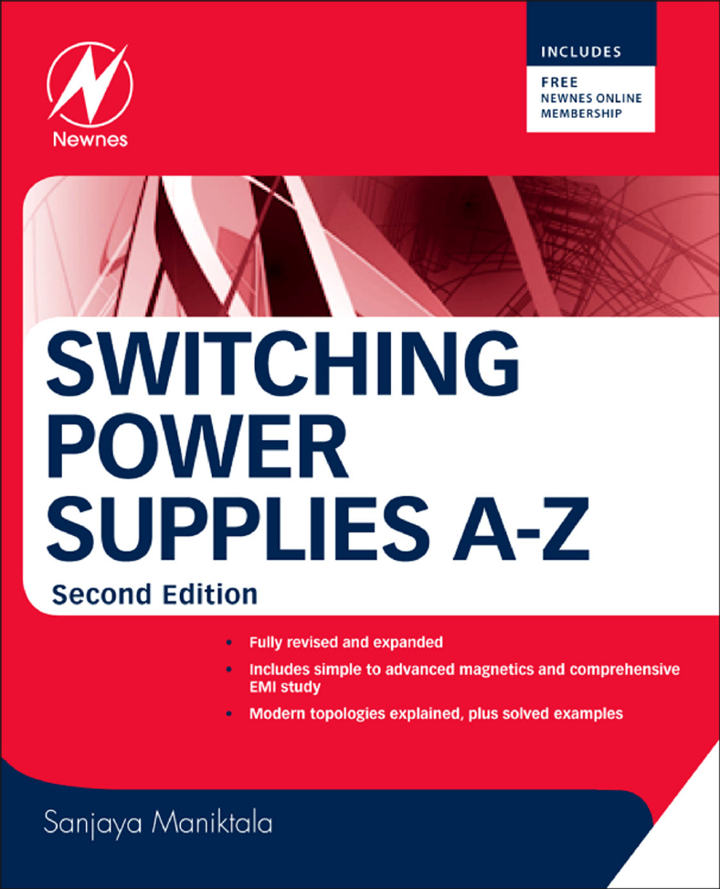
Front Cover
Switching Power Supplies A–Z
Copyright page
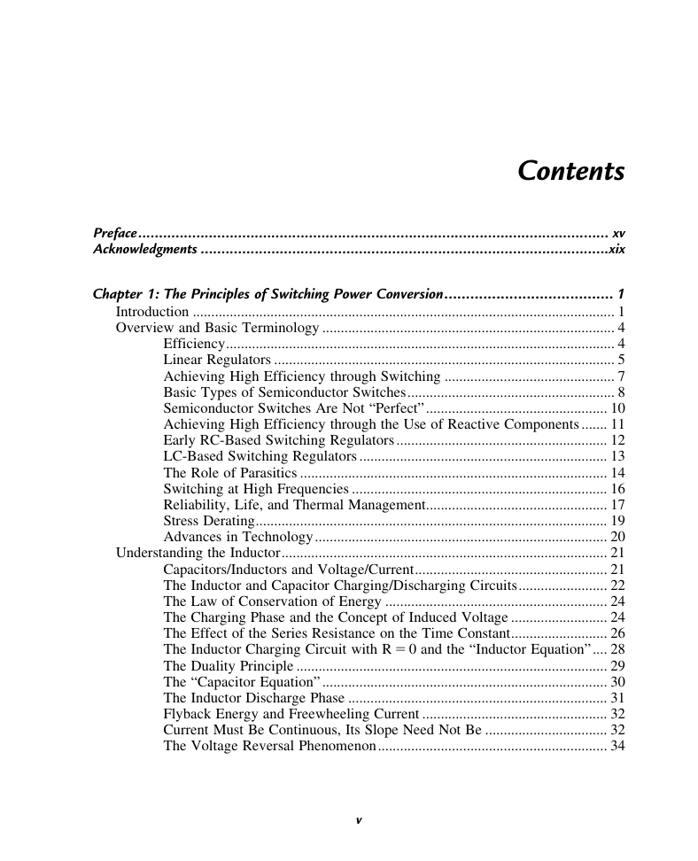
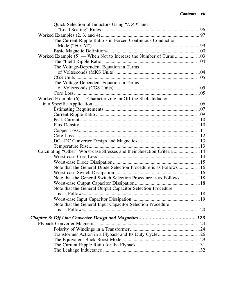
Contents
Preface
Acknowledgments
1 The Principles of Switching Power Conversion
Introduction
Overview and Basic Terminology
Efficiency
Linear Regulators
Achieving High Efficiency through Switching
Basic Types of Semiconductor Switches
Semiconductor Switches Are Not “Perfect”
Achieving High Efficiency through the Use of Reactive Components
Early RC-Based Switching Regulators
LC-Based Switching Regulators
The Role of Parasitics
Switching at High Frequencies
Reliability, Life, and Thermal Management
Stress Derating
Advances in Technology
Understanding the Inductor
Capacitors/Inductors and Voltage/Current
The Inductor and Capacitor Charging/Discharging Circuits
The Law of Conservation of Energy
The Charging Phase and the Concept of Induced Voltage
The Effect of the Series Resistance on the Time Constant
The Inductor Charging Circuit with R = 0 and the “Inductor Equation”
The Duality Principle
The “Capacitor Equation”
The Inductor Discharge Phase
Flyback Energy and Freewheeling Current
Current Must Be Continuous, Its Slope Need Not Be
The Voltage Reversal Phenomenon
A Steady State in Power Conversion and the Different Operating Modes
The Voltseconds Law, Inductor Reset and Converter Duty Cycle
Using and Protecting Semiconductor Switches
Evolution of Switching Topologies
Controlling the Induced Voltage Spike by Diversion through a Diode
Achieving a Steady State and Deriving Useful Energy
The Buck-Boost Converter
Ground-Referencing Our Circuits
The Buck-Boost Configurations
The Switching Node
Analyzing the Buck-Boost
Properties of the Buck-Boost
Why Three Basic Topologies Only?
The Boost Topology
The Buck Topology
Advanced Converter Design
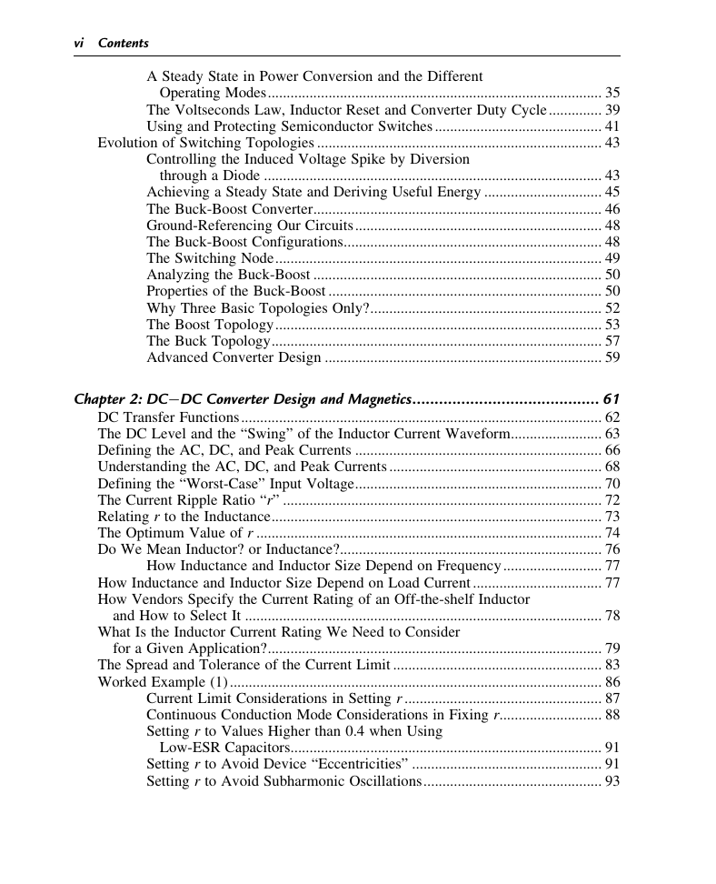
2 DC–DC Converter Design and Magnetics
DC Transfer Functions
The DC Level and the “Swing” of the Inductor Current Waveform
Defining the AC, DC, and Peak Currents
Understanding the AC, DC, and Peak Currents
Defining the “Worst-Case” Input Voltage
The Current Ripple Ratio “r”
Relating r to the Inductance
The Optimum Value of r
Do We Mean Inductor? or Inductance?
How Inductance and Inductor Size Depend on Frequency
How Inductance and Inductor Size Depend on Load Current
How Vendors Specify the Current Rating of an Off-the-shelf Inductor and How to Select It
What Is the Inductor Current Rating We Need to Consider for a Given Application?
The Spread and Tolerance of the Current Limit
Worked Example (1)
Current Limit Considerations in Setting r
Continuous Conduction Mode Considerations in Fixing r
Setting r to Values Higher than 0.4 when Using Low-ESR Capacitors
Setting r to Avoid Device “Eccentricities”
Setting r to Avoid Subharmonic Oscillations
Quick Selection of Inductors Using “L×I” and “Load Scaling” Rules
Worked Examples (2, 3, and 4)
The Current Ripple Ratio r in Forced Continuous Conduction Mode (“FCCM”)
Basic Magnetic Definitions
Worked Example (5) — When Not to Increase the Number of Turns
The “Field Ripple Ratio”
The Voltage-Dependent Equation in Terms of Voltseconds (MKS Units)
CGS Units
The Voltage-Dependent Equation in Terms of Voltseconds (CGS Units)
Core Loss
Worked Example (6) — Characterizing an Off-the-Shelf Inductor in a Specific Application
Estimating Requirements
Current Ripple Ratio
Peak Current
Flux Density
Copper Loss
Core Loss
DC–DC Converter Design and Magnetics
Temperature Rise
Calculating “Other” Worst-case Stresses and their Selection Criteria
Worst-case Core Loss
Worst-case Diode Dissipation
Note that the General Diode Selection Procedure is as Follows
Worst-case Switch Dissipation
Note that the General Switch Selection Procedure is as Follows
Worst-case Output Capacitor Dissipation
Note that the General Output Capacitor Selection Procedure is as Follows
Worst-case Input Capacitor Dissipation
Note that the General Input Capacitor Selection Procedure is as Follows
3 Off-Line Converter Design and Magnetics
Flyback Converter Magnetics
Polarity of Windings in a Transformer
Transformer Action in a Flyback and Its Duty Cycle
The Equivalent Buck-Boost Models
The Current Ripple Ratio for the Flyback
The Leakage Inductance
Zener Clamp Dissipation
Secondary-Side Leakages also Affect the Primary Side
Measuring the Effective Primary-side Leakage Inductance
Worked Example (7) — Designing the Flyback Transformer
Fixing the VOR and Vz
Turns Ratio
Maximum Duty Cycle (theoretical)
Effective Load Current on Primary and Secondary Sides
Duty Cycle
Actual Center of Primary and Secondary Current Ramps
Peak Switch Current
Voltseconds
Primary-Side Inductance
Selecting the Core
Number of Turns
Actual B-Field
Air Gap
Selecting the Wire Gauge and Foil Thickness
Forward Converter Magnetics
Duty Cycle
Worst-Case Input Voltage End
Window Utilization
Relating Core Size to Its Power Throughput
Worked Example (8) — Designing the Forward Transformer
Input Power
Selection of Core
Skin Depth
Thermal Resistance
Maximum B-Field
Voltµseconds
Number of Turns
Secondary Foil Thickness and Losses
Primary Winding and Losses
First Iteration
Second Iteration
Third Iteration
Fourth Iteration
Total Transformer Losses
4 The Topology FAQ
Questions and Answers
5 Advanced Magnetics: Optimal Core Selection
Part 1: Energy Transfer Principles
Overview of Topologies
The Energy Transfer Charts
Peak Energy Storage Requirements
Calculating Inductance Based on Desired Current Ripple
Part 2: Energy to Core Sizes
Magnetic Circuits and the Effective Length of Gapped Cores
Stored Energy in Gapped Cores and the z-Factor
Energy of a Gapped Core in Terms of the Volume of the Core
Part 3: Toroids to E-Cores
Part 4: More on AC–DC Flyback Transformer Design
Part 5: More on AC–DC Forward Converter Transformer Design
6 Component Ratings, Stresses, Reliability, and Life
Introduction
Stresses and Derating
Part 1: Ratings and Derating in Power Converter Applications
Operating Environments
Component Ratings and Stress Factors in Power Supplies
Diodes
MOSFETs
Capacitors
PCB
Mechanical Stresses
Part 2: MTBF, Failure Rate, Warranty Costs, and Life
MTBF
Warranty Costs
Life Expectancy and Failure Criteria
Reliability Prediction Methods
Demonstrated Reliability Testing (DRT)
Accelerated Life Testing
Part 3: Life Prediction of Aluminum Electrolytic Capacitors
7 Optimal Power Components Selection
Overview
The Key Stresses in Power Converters
Waveforms and Peak Voltage Stresses for Different Topologies
The Importance of RMS and Average Currents
Calculation of RMS and Average Currents for Diode, FET, and Inductor
Calculation of RMS and Average Currents for Capacitors
The Stress Spiders
Stress Reduction in AC–DC Converters
RCD Clamps versus RCD Snubbers
8 Conduction and Switching Losses
Switching a Resistive Load
Switching an Inductive Load
Switching Losses and Conduction Loss
A Simplified Model of the MOSFET for Studying Inductive Switching Losses
The Parasitic Capacitances Expressed in an Alternate System
Gate Threshold Voltage
The Turn-On Transition
The Turn-Off Transition
Gate Charge Factors
Worked Example
Turn-On
Turn-Off
Applying the Switching Loss Analysis to Switching Topologies
Worst-Case Input Voltage for Switching Losses
How Switching Losses Vary with the Parasitic Capacitances
Optimizing Driver Capability vis-à-vis MOSFET Characteristics
9 Discovering New Topologies
Part 1: Fixed-Frequency Synchronous Buck Topology
Using a FET (Safely) Instead of Diode
Birth of Dead Time
CdV/dt-Induced Turn-On
Counting on the Body-Diode
External (Paralleled) Schottky Diode
Synchronous (Complementary) Drive
Part 2: Fixed-Frequency Synchronous Boost Topology
Part 3: Current-Sensing Categories and General Techniques
DCR Sensing
The Inductorless Buck Cell
Lossless Droop Regulation and Dynamic Voltage Positioning
Part 4: The Four-Switch Buck-Boost
Part 5: Auxiliary Rails and Composite Topologies
Is It a Boost or Is It a Buck-Boost?
Understanding the Cuk, Sepic, and Zeta Topologies
Generating the Current Waveforms of the Cuk, Sepic, and Zeta Converters
Stresses in the Cuk, Sepic, and Zeta Topologies and Component Selection Criteria
Part 6: Configurations and “Topology Morphology”
Part 7: Other Topologies and Techniques
Hidden Auxiliary Rails and Symmetry
Multiple Outputs and the Floating Buck Regulator
Hysteretic Controllers
Pulse-Skipping Mode
Achieving Transformer Reset in Forward Converters
10 Printed Circuit Board Layout
Introduction
Trace Section Analysis
Some Points to Keep in Mind During Layout
Thermal Management Concerns
11 Thermal Management
Thermal Resistance and Board Construction
Historical Definitions
Empirical Equations for Natural Convection
Comparing the Two Standard Empirical Equations
“h” from Thermodynamic Theory
PCB Copper Area Estimate
Sizing Copper Traces
Natural Convection at an Altitude
Forced Air Cooling
Radiative Heat Transfer
Miscellaneous Issues
12 Feedback Loop Analysis and Stability
Transfer Functions, Time Constant, and the Forcing Function
Understanding “e” and Plotting Curves on Log Scales
Flashback: Complex Representation
Repetitive and Nonrepetitive Stimuli: Time Domain and Frequency Domain Analyses
The s-Plane
Laplace Transform Method
Disturbances and the Role of Feedback
Transfer Function of the RC Filter, Gain, and the Bode Plot
The Integrator Op-amp (“Pole-at-Zero” Filter)
Mathematics in the Log-Plane
Transfer Function of the Post-LC Filter
Summary of Transfer Functions of Passive Filters
Poles and Zeros
“Interactions” of Poles and Zeros
Closed and Open-Loop Gain
The Voltage Divider
Pulse-Width Modulator Transfer Function
Voltage (Line) Feedforward
Power Stage Transfer Function
Plant Transfer Functions of All the Topologies
Feedback-Stage Transfer Functions
Closing the Loop
Criteria and Strategy for Ensuring Loop Stability
Plotting the Open-Loop Gain for the Three Topologies
The ESR-Zero
High-Frequency Pole
Designing a Type 3 Op-Amp Compensation Network
Optimizing the Feedback Loop
Input Ripple Rejection
Load Transients
Type 1 and Type 2 Compensations
Transconductance Op-Amp Compensation
Simpler Transconductance Op-Amp Compensation
Compensating with Current-Mode Control
13 Advanced Topics: Paralleling, Interleaving, and Load Sharing
Part 1: Voltage Ripple of Converters
Buck Converter Input and Output Voltage Ripple
Part 2: Distributing and Reducing Stresses in Power Converters
Overview
Power Scaling Guidelines in Power Converters
Concept behind Paralleling and Interleaving of Buck Converters
Closed-Form Equations for RMS Stresses of Interleaved Buck Converter
Interleaved Boost PFC Converters
Interleaved Multioutput Converters
Part 3: Coupled Inductors in Interleaved Buck Converters
Overview
Part 4: Load Sharing in Paralleled Converters
Passive Sharing
Active Load Sharing
14 The Front End of AC–DC Power Supplies
Overview
Part 1: Low-Power Applications
The Charging and Discharging Phases
Increasing the Capacitance, Thereby Reducing tCOND, Causes High RMS Currents
The Capacitor Voltage Trajectory and the Basic Intervals
Tolerating High Input Voltage Ripple in AC–DC Switching Converters
How the Bulk Capacitor Voltage Ripple Impacts the Switching Converter Design
General Flyback Fault Protection Schemes
The Input Current Shape and the Capacitor Current
How to Interpret μF/W correctly
Worked Example using either Quick Lookup Numbers or the “Arctic Analogy”
Accounting for Capacitor Tolerances and Life
Holdup Time Considerations
Two Different Flyback Design Strategies for Meeting Holdup Requirements
Part 2: High-Power Applications and PFC
Overview
How to get a Boost Topology to exhibit a Sine-wave Input Current?
Anti-Synchronization Technique for PFC and PWM Stages
Capacitor RMS Current Calculations With and Without Anti-Synchronization
Interleaved Boost PFC Stages
Practical Issues in Designing PFC Stages
PFC Choke Design Guidelines
Core Losses in PFC Choke
Borderline Active PFC using Boost
15 EMI Standards and Measurements
Part 1: Overview and Limits
The Standards
EMI Limits
Some Cost-Related Rules-of-Thumb
EMI for Subassemblies
Electromagnetic Waves and Fields
Extrapolation
Quasi-Peak, Average, and Peak Measurements
Part 2: Measurements of Conducted EMI
Differential Mode and Common Mode Noise
Measuring Conducted EMI with a LISN
Simple Math for Estimating Maximum Conducted Noise Currents
Separating CM and DM Components for Conducted EMI Diagnostics
Near-Field Sniffers for Radiated EMI Diagnostics
16 Practical EMI Line Filters and Noise Sources in Power Supplies
Part 1: Practical Line Filters
Basic Safety Issues in EMI Filter Design
Safety Restrictions on the Total Y-Capacitance
Practical Line Filters
Examining the Equivalent DM and CM Circuits and Filter Design Hints
The Ground Choke
Some Notable Industry Experiences in EMI Filter Design
Part 2: DM and CM Noise in Switching Power Supplies
Main Source of DM Noise
The Main Source of CM Noise
Chassis-Mounting of Semiconductors
The CM Noise Source
The Road to Cost-Effective Filter Design
17 Fixing EMI Across the Board and Input Filter Instability
Part 1: Practical Techniques for EMI Mitigation
The Ground Plane
The Role of the Transformer in EMI
EMI from Diodes
Are We Going to Fail the Radiation Test?
Part 2: Modules and Input Instability
Practical Line Filters in DC–DC Converter Modules
18 The Math Behind the Electromagnetic Puzzle
Fourier Series in Power Supplies
The Rectangular Wave
The Sinc Function
The Envelope of the Fourier Amplitudes
Practical DM Filter Design
ESR Estimate
DM Calculations at High Line
DM Calculations at Low Line
Filter Safety Margin
Practical CM Filter Design
CM Calculations at High Line
19 Solved Examples
Part 1: FET Selection
Part 2: Conduction Losses in the FETs
Part 3: FET Switching Losses
Part 4: Inductor Loss
Part 5: Input Capacitor Selection and Loss
Part 6: Output Capacitor Selection and Loss
Part 7: Total Losses and Efficiency Estimate
Part 8: Junction Temperature Estimates
Part 9: Control Loop Design
Appendix
Further Reading
Index





 2023年江西萍乡中考道德与法治真题及答案.doc
 2012年重庆南川中考生物真题及答案.doc
 2013年江西师范大学地理学综合及文艺理论基础考研真题.doc
 2020年四川甘孜小升初语文真题及答案I卷.doc
 2020年注册岩土工程师专业基础考试真题及答案.doc
 2023-2024学年福建省厦门市九年级上学期数学月考试题及答案.doc
 2021-2022学年辽宁省沈阳市大东区九年级上学期语文期末试题及答案.doc
 2022-2023学年北京东城区初三第一学期物理期末试卷及答案.doc
 2018上半年江西教师资格初中地理学科知识与教学能力真题及答案.doc
 2012年河北国家公务员申论考试真题及答案-省级.doc
 2020-2021学年江苏省扬州市江都区邵樊片九年级上学期数学第一次质量检测试题及答案.doc
 2022下半年黑龙江教师资格证中学综合素质真题及答案.doc