JEDEC Standard No. 21-C
Page 4.1.2.12.2 – 1
Annex L: Serial Presence Detect (SPD) for DDR4 SDRAM Modules
DDR4 SPD Document Release 2
UDIMM Revision 1.0
RDIMM Revision 1.0
LRDIMM Revision 1.0
1.0 Introduction
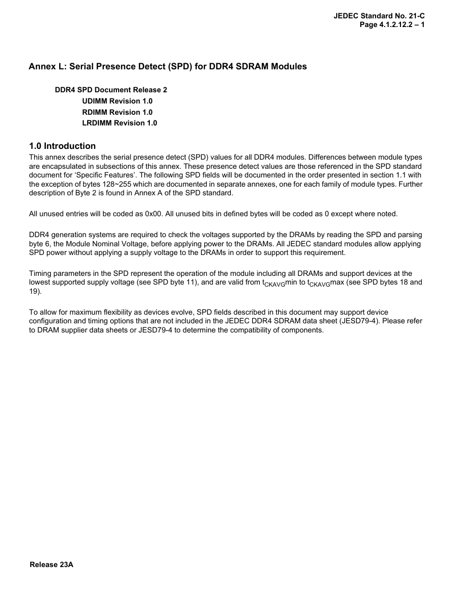
This annex describes the serial presence detect (SPD) values for all DDR4 modules. Differences between module types
are encapsulated in subsections of this annex. These presence detect values are those referenced in the SPD standard
document for ‘Specific Features’. The following SPD fields will be documented in the order presented in section 1.1 with
the exception of bytes 128~255 which are documented in separate annexes, one for each family of module types. Further
description of Byte 2 is found in Annex A of the SPD standard.
All unused entries will be coded as 0x00. All unused bits in defined bytes will be coded as 0 except where noted.
DDR4 generation systems are required to check the voltages supported by the DRAMs by reading the SPD and parsing
byte 6, the Module Nominal Voltage, before applying power to the DRAMs. All JEDEC standard modules allow applying
SPD power without applying a supply voltage to the DRAMs in order to support this requirement.
Timing parameters in the SPD represent the operation of the module including all DRAMs and support devices at the
lowest supported supply voltage (see SPD byte 11), and are valid from tCKAVGmin to tCKAVGmax (see SPD bytes 18 and
19).
To allow for maximum flexibility as devices evolve, SPD fields described in this document may support device
configuration and timing options that are not included in the JEDEC DDR4 SDRAM data sheet (JESD79-4). Please refer
to DRAM supplier data sheets or JESD79-4 to determine the compatibility of components.
Release 23A
�
JEDEC Standard No. 21-C
Page 4.1.2.12.2 – 2
1.1 Address map
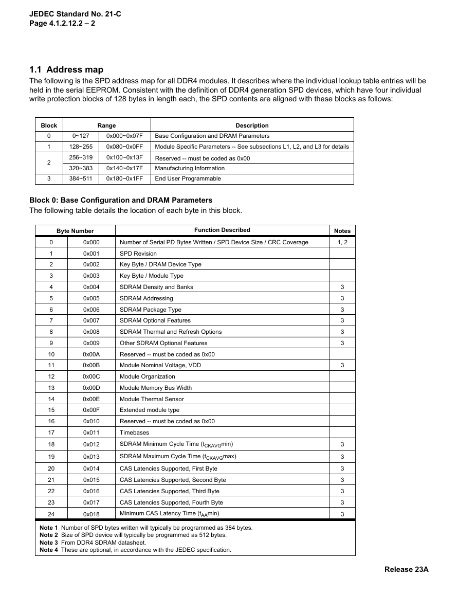
The following is the SPD address map for all DDR4 modules. It describes where the individual lookup table entries will be
held in the serial EEPROM. Consistent with the definition of DDR4 generation SPD devices, which have four individual
write protection blocks of 128 bytes in length each, the SPD contents are aligned with these blocks as follows:
Block
Range
0
1
2
3
0~127
128~255
256~319
320~383
384~511
0x000~0x07F
0x080~0x0FF
0x100~0x13F
0x140~0x17F
0x180~0x1FF
Description
Base Configuration and DRAM Parameters
Module Specific Parameters -- See subsections L1, L2, and L3 for details
Reserved -- must be coded as 0x00
Manufacturing Information
End User Programmable
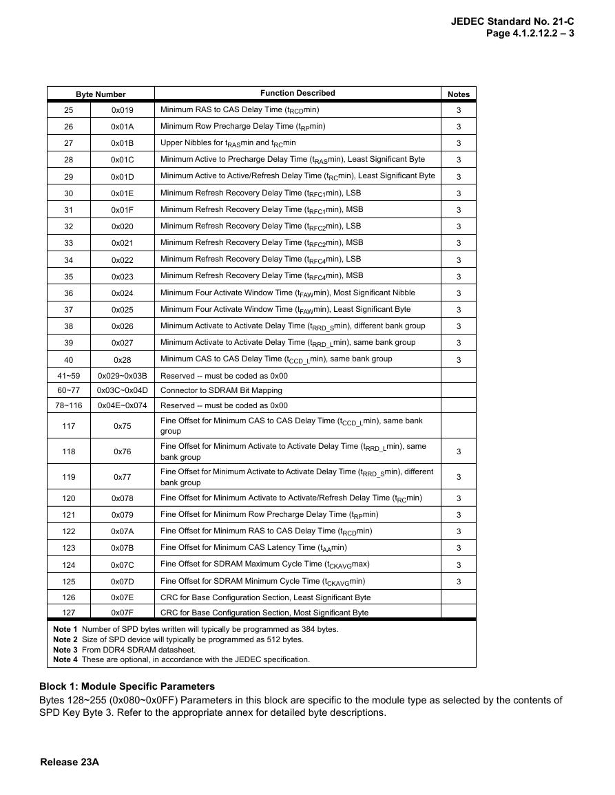
Block 0: Base Configuration and DRAM Parameters
The following table details the location of each byte in this block.
Byte Number
Function Described
0
1
2
3
4
5
6
7
8
9
10
11
12
13
14
15
16
17
18
19
20
21
22
23
24
0x000
0x001
0x002
0x003
0x004
0x005
0x006
0x007
0x008
0x009
0x00A
0x00B
0x00C
0x00D
0x00E
0x00F
0x010
0x011
0x012
0x013
0x014
0x015
0x016
0x017
0x018
Number of Serial PD Bytes Written / SPD Device Size / CRC Coverage
SPD Revision
Key Byte / DRAM Device Type
Key Byte / Module Type
SDRAM Density and Banks
SDRAM Addressing
SDRAM Package Type
SDRAM Optional Features
SDRAM Thermal and Refresh Options
Other SDRAM Optional Features
Reserved -- must be coded as 0x00
Module Nominal Voltage, VDD
Module Organization
Module Memory Bus Width
Module Thermal Sensor
Extended module type
Reserved -- must be coded as 0x00
Timebases
SDRAM Minimum Cycle Time (tCKAVGmin)
SDRAM Maximum Cycle Time (tCKAVGmax)
CAS Latencies Supported, First Byte
CAS Latencies Supported, Second Byte
CAS Latencies Supported, Third Byte
CAS Latencies Supported, Fourth Byte
Minimum CAS Latency Time (tAAmin)
Note 1 Number of SPD bytes written will typically be programmed as 384 bytes.
Note 2 Size of SPD device will typically be programmed as 512 bytes.
Note 3 From DDR4 SDRAM datasheet.
Note 4 These are optional, in accordance with the JEDEC specification.
Notes
1, 2
3
3
3
3
3
3
3
3
3
3
3
3
3
3
Release 23A
�
JEDEC Standard No. 21-C
Page 4.1.2.12.2 – 3
Byte Number
Function Described
Notes
25
26
27
28
29
30
31
32
33
34
35
36
37
38
39
40
0x019
0x01A
0x01B
0x01C
0x01D
0x01E
0x01F
0x020
0x021
0x022
0x023
0x024
0x025
0x026
0x027
0x28
41~59
60~77
78~116
0x029~0x03B
0x03C~0x04D
0x04E~0x074
117
118
119
120
121
122
123
124
125
126
127
0x75
0x76
0x77
0x078
0x079
0x07A
0x07B
0x07C
0x07D
0x07E
0x07F
Minimum RAS to CAS Delay Time (tRCDmin)
Minimum Row Precharge Delay Time (tRPmin)
Upper Nibbles for tRASmin and tRCmin
Minimum Active to Precharge Delay Time (tRASmin), Least Significant Byte
Minimum Active to Active/Refresh Delay Time (tRCmin), Least Significant Byte
Minimum Refresh Recovery Delay Time (tRFC1min), LSB
Minimum Refresh Recovery Delay Time (tRFC1min), MSB
Minimum Refresh Recovery Delay Time (tRFC2min), LSB
Minimum Refresh Recovery Delay Time (tRFC2min), MSB
Minimum Refresh Recovery Delay Time (tRFC4min), LSB
Minimum Refresh Recovery Delay Time (tRFC4min), MSB
Minimum Four Activate Window Time (tFAWmin), Most Significant Nibble
Minimum Four Activate Window Time (tFAWmin), Least Significant Byte
Minimum Activate to Activate Delay Time (tRRD_Smin), different bank group
Minimum Activate to Activate Delay Time (tRRD_Lmin), same bank group
Minimum CAS to CAS Delay Time (tCCD_Lmin), same bank group
Reserved -- must be coded as 0x00
Connector to SDRAM Bit Mapping
Reserved -- must be coded as 0x00
Fine Offset for Minimum CAS to CAS Delay Time (tCCD_Lmin), same bank
group
Fine Offset for Minimum Activate to Activate Delay Time (tRRD_Lmin), same
bank group
Fine Offset for Minimum Activate to Activate Delay Time (tRRD_Smin), different
bank group
Fine Offset for Minimum Activate to Activate/Refresh Delay Time (tRCmin)
Fine Offset for Minimum Row Precharge Delay Time (tRPmin)
Fine Offset for Minimum RAS to CAS Delay Time (tRCDmin)
Fine Offset for Minimum CAS Latency Time (tAAmin)
Fine Offset for SDRAM Maximum Cycle Time (tCKAVGmax)
Fine Offset for SDRAM Minimum Cycle Time (tCKAVGmin)
CRC for Base Configuration Section, Least Significant Byte
CRC for Base Configuration Section, Most Significant Byte
Note 1 Number of SPD bytes written will typically be programmed as 384 bytes.
Note 2 Size of SPD device will typically be programmed as 512 bytes.
Note 3 From DDR4 SDRAM datasheet.
Note 4 These are optional, in accordance with the JEDEC specification.
3
3
3
3
3
3
3
3
3
3
3
3
3
3
3
3
3
3
3
3
3
3
3
3
Block 1: Module Specific Parameters
Bytes 128~255 (0x080~0x0FF) Parameters in this block are specific to the module type as selected by the contents of
SPD Key Byte 3. Refer to the appropriate annex for detailed byte descriptions.
Release 23A
�
JEDEC Standard No. 21-C
Page 4.1.2.12.2 – 4
Block 2, lower half: Reserved
Bytes 256~319 (0x100~0x13F) Reserved -- must be coded as 0x00.
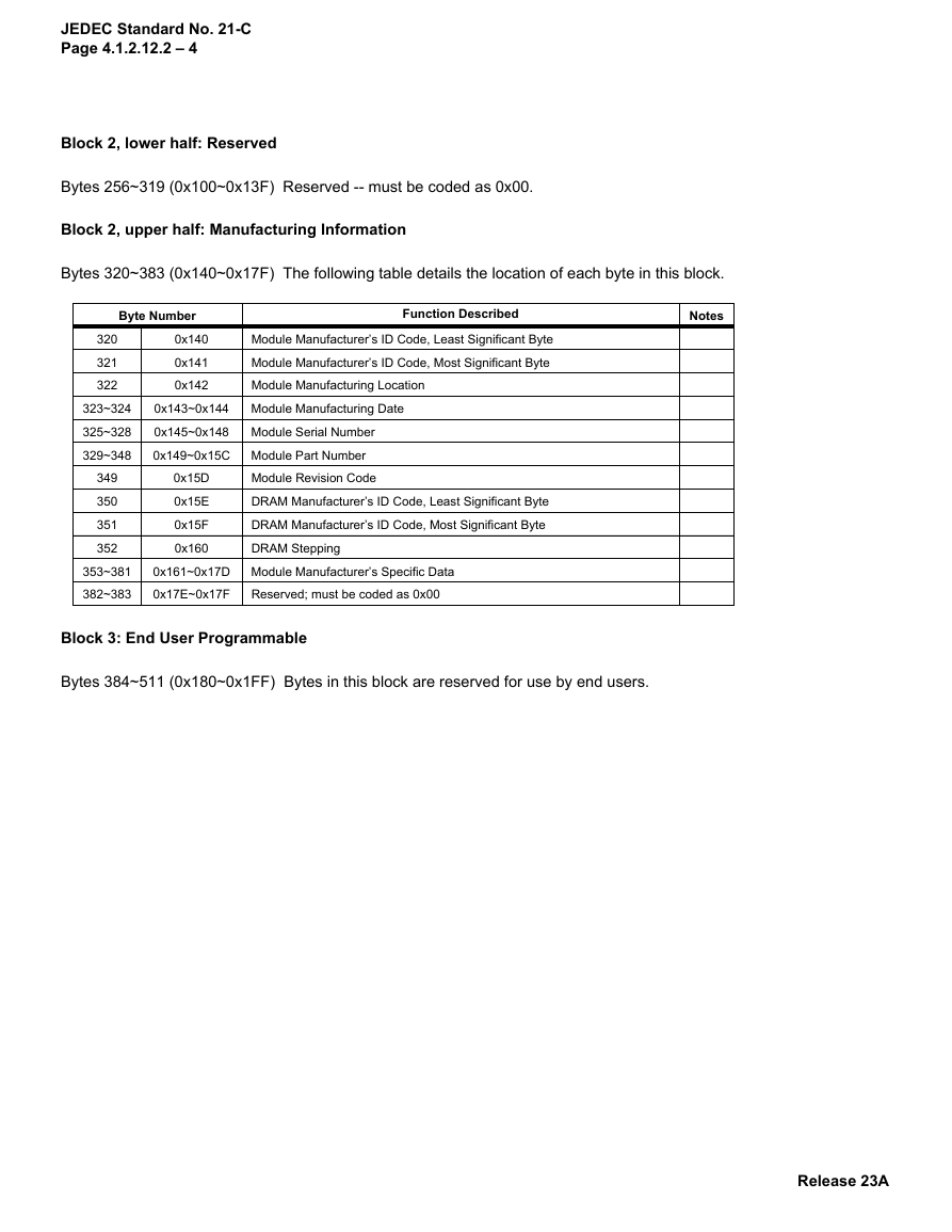
Block 2, upper half: Manufacturing Information
Bytes 320~383 (0x140~0x17F) The following table details the location of each byte in this block.
Byte Number
320
321
322
0x140
0x141
0x142
323~324
325~328
329~348
0x143~0x144
0x145~0x148
0x149~0x15C
349
350
351
352
0x15D
0x15E
0x15F
0x160
353~381
382~383
0x161~0x17D
0x17E~0x17F
Function Described
Notes
Module Manufacturer’s ID Code, Least Significant Byte
Module Manufacturer’s ID Code, Most Significant Byte
Module Manufacturing Location
Module Manufacturing Date
Module Serial Number
Module Part Number
Module Revision Code
DRAM Manufacturer’s ID Code, Least Significant Byte
DRAM Manufacturer’s ID Code, Most Significant Byte
DRAM Stepping
Module Manufacturer’s Specific Data
Reserved; must be coded as 0x00
Block 3: End User Programmable
Bytes 384~511 (0x180~0x1FF) Bytes in this block are reserved for use by end users.
Release 23A
�
JEDEC Standard No. 21-C
Page 4.1.2.12.2 – 5
2.0 Details of each byte
2.1 General Configuration Section: Bytes 0~127 (0x000~0x07F)
This section contains defines parameters that are common to all DDR4 module types.
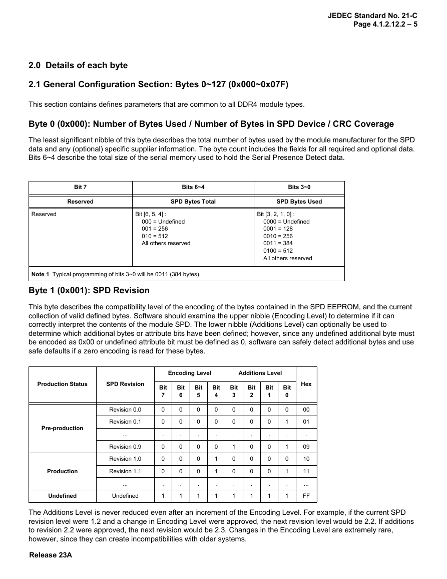
Byte 0 (0x000): Number of Bytes Used / Number of Bytes in SPD Device / CRC Coverage
The least significant nibble of this byte describes the total number of bytes used by the module manufacturer for the SPD
data and any (optional) specific supplier information. The byte count includes the fields for all required and optional data.
Bits 6~4 describe the total size of the serial memory used to hold the Serial Presence Detect data.
Bit 7
Reserved
Bits 6~4
SPD Bytes Total
Reserved
Bit [6, 5, 4] :
000 = Undefined
001 = 256
010 = 512
All others reserved
Bits 3~0
SPD Bytes Used
Bit [3, 2, 1, 0] :
0000 = Undefined
0001 = 128
0010 = 256
0011 = 384
0100 = 512
All others reserved
Note 1 Typical programming of bits 3~0 will be 0011 (384 bytes).
Byte 1 (0x001): SPD Revision
This byte describes the compatibility level of the encoding of the bytes contained in the SPD EEPROM, and the current
collection of valid defined bytes. Software should examine the upper nibble (Encoding Level) to determine if it can
correctly interpret the contents of the module SPD. The lower nibble (Additions Level) can optionally be used to
determine which additional bytes or attribute bits have been defined; however, since any undefined additional byte must
be encoded as 0x00 or undefined attribute bit must be defined as 0, software can safely detect additional bytes and use
safe defaults if a zero encoding is read for these bytes.
Production Status
SPD Revision
Pre-production
Production
Undefined
Revision 0.0
Revision 0.1
...
Revision 0.9
Revision 1.0
Revision 1.1
...
Undefined
Encoding Level
Additions Level
Bit
7
Bit
6
Bit
5
Bit
4
Bit
3
Bit
2
Bit
1
Bit
0
0
0
.
0
0
0
.
1
0
0
.
0
0
0
.
1
0
0
.
0
0
0
.
1
0
0
.
0
1
1
.
1
0
0
.
1
0
0
.
1
0
0
.
0
0
0
.
1
0
0
.
0
0
0
.
1
0
1
.
1
0
1
.
1
Hex
00
01
.
09
10
11
...
FF
The Additions Level is never reduced even after an increment of the Encoding Level. For example, if the current SPD
revision level were 1.2 and a change in Encoding Level were approved, the next revision level would be 2.2. If additions
to revision 2.2 were approved, the next revision would be 2.3. Changes in the Encoding Level are extremely rare,
however, since they can create incompatibilities with older systems.
Release 23A
�
JEDEC Standard No. 21-C
Page 4.1.2.12.2 – 6
The exceptions to the above rule are the SPD revision levels used during development prior to the Revision 1.0 release.
Revisions 0.0 through 0.9 are used to indicate sequential pre-production SPD revision levels, however the first production
release will be Revision 1.0.
This document defines the SPD contents for multiple families of DDR4 memory modules, with a separate subsection of
this Annex for each family that defines the bytes in SPD locations 128~255 (0x080~0x0FF). These module families and
their respective subsections are:
• Annex L.1: Unbuffered Memory Modules
• Annex L.2: Registered Memory Modules
• Annex L.3: Load Reduced Memory Modules
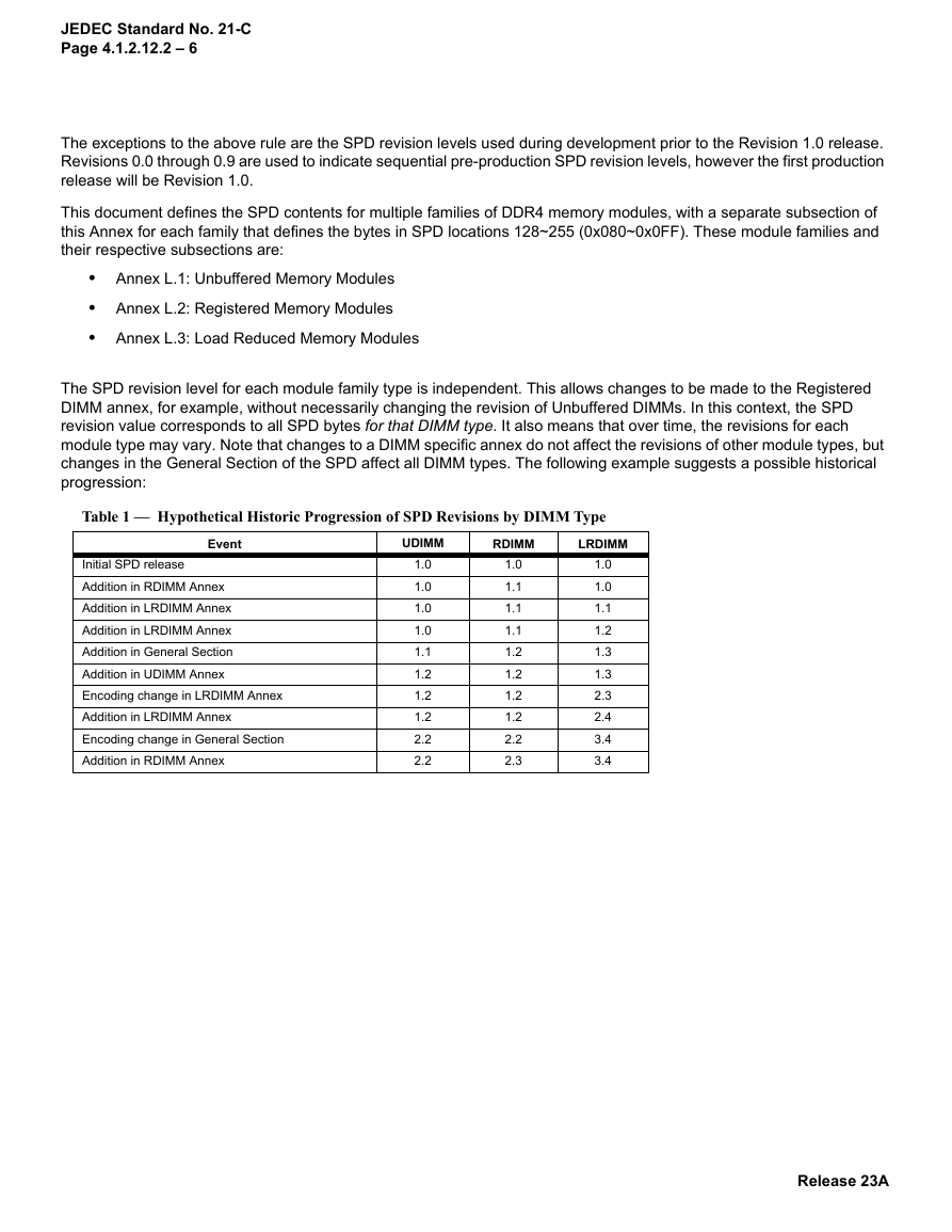
The SPD revision level for each module family type is independent. This allows changes to be made to the Registered
DIMM annex, for example, without necessarily changing the revision of Unbuffered DIMMs. In this context, the SPD
revision value corresponds to all SPD bytes for that DIMM type. It also means that over time, the revisions for each
module type may vary. Note that changes to a DIMM specific annex do not affect the revisions of other module types, but
changes in the General Section of the SPD affect all DIMM types. The following example suggests a possible historical
progression:
Table 1 — Hypothetical Historic Progression of SPD Revisions by DIMM Type
Event
UDIMM
RDIMM
LRDIMM
Initial SPD release
Addition in RDIMM Annex
Addition in LRDIMM Annex
Addition in LRDIMM Annex
Addition in General Section
Addition in UDIMM Annex
Encoding change in LRDIMM Annex
Addition in LRDIMM Annex
Encoding change in General Section
Addition in RDIMM Annex
1.0
1.0
1.0
1.0
1.1
1.2
1.2
1.2
2.2
2.2
1.0
1.1
1.1
1.1
1.2
1.2
1.2
1.2
2.2
2.3
1.0
1.0
1.1
1.2
1.3
1.3
2.3
2.4
3.4
3.4
Release 23A
�
JEDEC Standard No. 21-C
Page 4.1.2.12.2 – 7
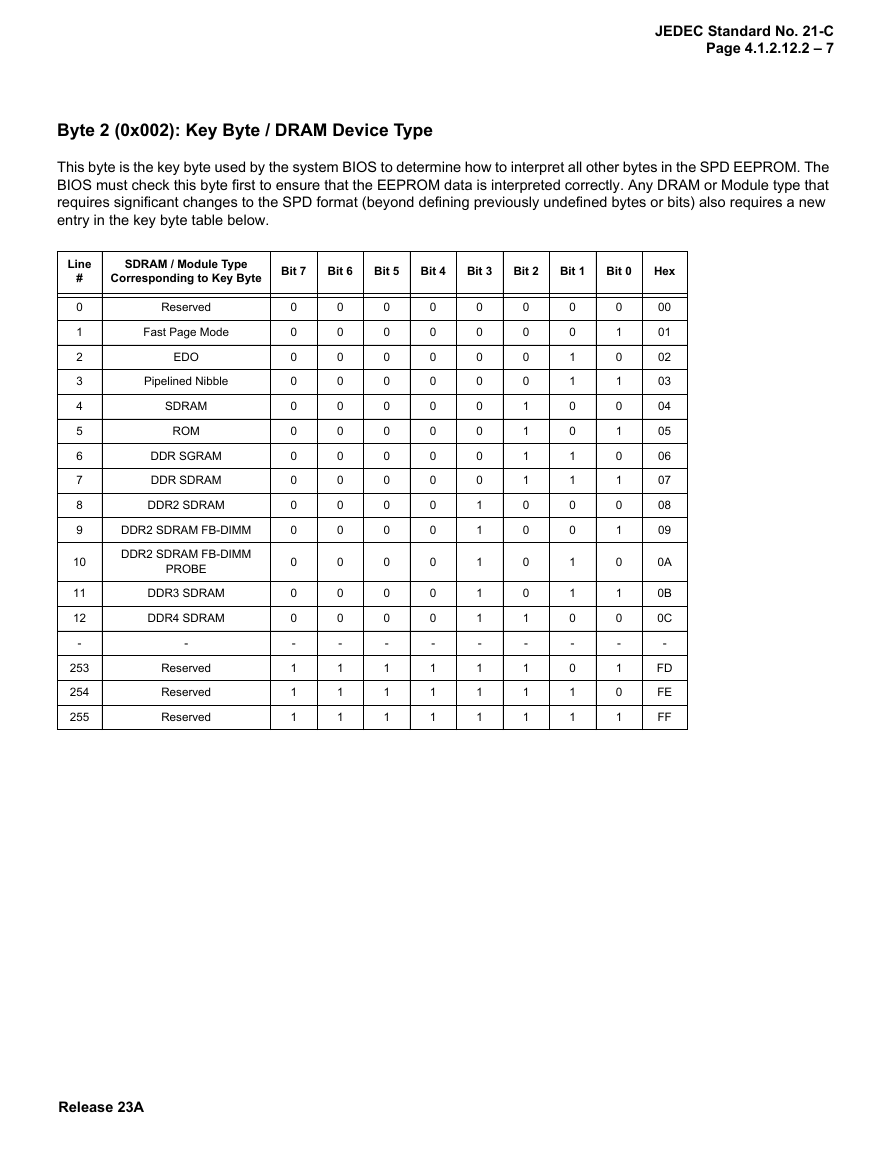
Byte 2 (0x002): Key Byte / DRAM Device Type
This byte is the key byte used by the system BIOS to determine how to interpret all other bytes in the SPD EEPROM. The
BIOS must check this byte first to ensure that the EEPROM data is interpreted correctly. Any DRAM or Module type that
requires significant changes to the SPD format (beyond defining previously undefined bytes or bits) also requires a new
entry in the key byte table below.
Line
#
SDRAM / Module Type
Corresponding to Key Byte
Bit 7
Bit 6
Bit 5
Bit 4
Bit 3
Bit 2
Bit 1
Bit 0
Hex
0
1
2
3
4
5
6
7
8
9
10
11
12
-
253
254
255
Reserved
Fast Page Mode
EDO
Pipelined Nibble
SDRAM
ROM
DDR SGRAM
DDR SDRAM
DDR2 SDRAM
DDR2 SDRAM FB-DIMM
DDR2 SDRAM FB-DIMM
PROBE
DDR3 SDRAM
DDR4 SDRAM
-
Reserved
Reserved
Reserved
0
0
0
0
0
0
0
0
0
0
0
0
0
-
1
1
1
0
0
0
0
0
0
0
0
0
0
0
0
0
-
1
1
1
0
0
0
0
0
0
0
0
0
0
0
0
0
-
1
1
1
0
0
0
0
0
0
0
0
0
0
0
0
0
-
1
1
1
0
0
0
0
0
0
0
0
1
1
1
1
1
-
1
1
1
0
0
0
0
1
1
1
1
0
0
0
0
1
-
1
1
1
0
0
1
1
0
0
1
1
0
0
1
1
0
-
0
1
1
0
1
0
1
0
1
0
1
0
1
0
1
0
-
1
0
1
00
01
02
03
04
05
06
07
08
09
0A
0B
0C
-
FD
FE
FF
Release 23A
�
JEDEC Standard No. 21-C
Page 4.1.2.12.2 – 8
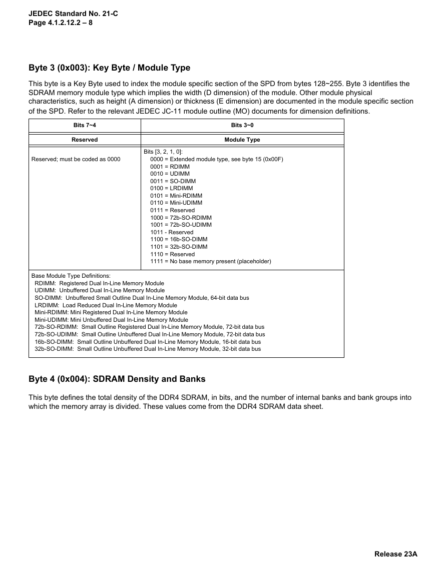
Byte 3 (0x003): Key Byte / Module Type
This byte is a Key Byte used to index the module specific section of the SPD from bytes 128~255. Byte 3 identifies the
SDRAM memory module type which implies the width (D dimension) of the module. Other module physical
characteristics, such as height (A dimension) or thickness (E dimension) are documented in the module specific section
of the SPD. Refer to the relevant JEDEC JC-11 module outline (MO) documents for dimension definitions.
Bits 7~4
Reserved
Bits 3~0
Module Type
Reserved; must be coded as 0000
Bits [3, 2, 1, 0]:
0000 = Extended module type, see byte 15 (0x00F)
0001 = RDIMM
0010 = UDIMM
0011 = SO-DIMM
0100 = LRDIMM
0101 = Mini-RDIMM
0110 = Mini-UDIMM
0111 = Reserved
1000 = 72b-SO-RDIMM
1001 = 72b-SO-UDIMM
1011 - Reserved
1100 = 16b-SO-DIMM
1101 = 32b-SO-DIMM
1110 = Reserved
1111 = No base memory present (placeholder)
Base Module Type Definitions:
RDIMM: Registered Dual In-Line Memory Module
UDIMM: Unbuffered Dual In-Line Memory Module
SO-DIMM: Unbuffered Small Outline Dual In-Line Memory Module, 64-bit data bus
LRDIMM: Load Reduced Dual In-Line Memory Module
Mini-RDIMM: Mini Registered Dual In-Line Memory Module
Mini-UDIMM: Mini Unbuffered Dual In-Line Memory Module
72b-SO-RDIMM: Small Outline Registered Dual In-Line Memory Module, 72-bit data bus
72b-SO-UDIMM: Small Outline Unbuffered Dual In-Line Memory Module, 72-bit data bus
16b-SO-DIMM: Small Outline Unbuffered Dual In-Line Memory Module, 16-bit data bus
32b-SO-DIMM: Small Outline Unbuffered Dual In-Line Memory Module, 32-bit data bus
Byte 4 (0x004): SDRAM Density and Banks
This byte defines the total density of the DDR4 SDRAM, in bits, and the number of internal banks and bank groups into
which the memory array is divided. These values come from the DDR4 SDRAM data sheet.
Release 23A
�


 2023年江西萍乡中考道德与法治真题及答案.doc
 2012年重庆南川中考生物真题及答案.doc
 2013年江西师范大学地理学综合及文艺理论基础考研真题.doc
 2020年四川甘孜小升初语文真题及答案I卷.doc
 2020年注册岩土工程师专业基础考试真题及答案.doc
 2023-2024学年福建省厦门市九年级上学期数学月考试题及答案.doc
 2021-2022学年辽宁省沈阳市大东区九年级上学期语文期末试题及答案.doc
 2022-2023学年北京东城区初三第一学期物理期末试卷及答案.doc
 2018上半年江西教师资格初中地理学科知识与教学能力真题及答案.doc
 2012年河北国家公务员申论考试真题及答案-省级.doc
 2020-2021学年江苏省扬州市江都区邵樊片九年级上学期数学第一次质量检测试题及答案.doc
 2022下半年黑龙江教师资格证中学综合素质真题及答案.doc