Essential Electronic Design Automation
(EDA)
By Mark D. Birnbaum
of
Publisher
Pub Date
ISBN
Pages
Slots
: Prentice Hall PTR
: October 01, 2003
: 0-13-182829-0
: 256
:
1.0
• Table
Contents
• Index
Essential Electronic Design Automation (EDA) demystifies this highly technical industry for
anyone with a "need-to-know" about EDA. A friendly, informal introduction to EDA business
and technology, clear enough for laypeople yet detailed enough for technical readers. The
book also makes an excellent complementary text for cross-disciplinary engineering,
business and marketing courses on VLSI Design.
Simply and clearly, veteran industry leader Mark Birnbaum introduces the design problems
EDA is intended to solve, the tools that exist to solve them, the designers who use them,
and what makes EDA crucial to electronic product and chip design.
•
• Explains how EDA fits into the electronic product and semiconductor industries
• Examines the EDA industry from both the tool user and EDA software vendor
perspectives, including business models, return on investment, and tool evaluation
Includes electronic system-level tools for defining what ICs will do, front -end
functional chip-level tools for design how the IC will behave, and back-end design
tools for implementing the IC physical layout
• Discusses EDA industry trends and IC design issues, including deep submicron
challenges, intellectual property (IP), and system-on-chip (SoC)
Includes EDA standards organizations and publications
•
Industry newcomers will appreciate the book's extensive set of appendices, including
primers on electricity, semiconductor manufacturing, computing, and common dimensions,
reference sources and a complete glossary with acronym pronunciation.
1
�
Preface
Purpose of This Book
Purpose of This Book
The tremendous increase in the use of tiny electronic devices is common knowledge. We find
them everywhere today, in cars, household appliances, telephones, music, and business
equipment. The typical car or house uses dozens of them.
These devices are called microchips or integrated circuits (ICs). Today a single IC can do
more than an entire roomful of equipment just a decade ago. Integrated circuits are small
enough to hold in your hand, yet contain millions of tiny electronic components.
Engineers create detailed design plans to make ICs, similar to an architect's building plans.
Architects use computer tools to design a building and predict the structure's response to
storms or earthquakes. Similarly, IC designers use computer program tools to design an IC,
test its performance, and verify its behavior. We refer to the tools as electronic design
automation (EDA) .
An entire industry has evolved to provide these tools to aid the IC designers. This book
introduces readers to the EDA industry. It discusses both the technical and business aspects
of EDA in clear non-technical language without equations. The text briefly describes the
related semiconductor industry issues and evolving chip design problems addressed by the
EDA tools. A unique, dialog format presents the technical material in an easy-to-read
manner.
The book focuses solely on EDA for IC design, intentionally excluding other design
automation areas (e.g., printed circuit boards and mechanical design). The text gives
generic tool descriptions since company and product names change rapidly.
Intended Audience
The electronic product industry consists of electronic system manufacturers, semiconductor
companies, and chip design houses. Semiconductor equipment providers, test equipment
manufacturers, and EDA companies are also part of the industry.
In most of these firms, over half the employees are non-technical or "semi-technical."
These semi-technical people are involved in the EDA or related industries. Experienced
e mployees will have picked up some jargon and knowledge, but both they and most new
employees lack an overall introduction to this highly technical field.
Sales and marketing, communications, legal, or finance personnel will find the book useful.
Others in financial analysis, public relations, or publications firms also need to know about
the EDA industry. Some readers will be interested only in the overview, business, or industry
sections, while others will focus on particular technical EDA chapters.
2
�
Along with the semi-technical people, many people with technical backgrounds will find
the book very beneficial. The technical backgrounds include computer engineering,
programming, electronic testing, mechanical engineering, packaging, or academic fields.
These readers may not have EDA backgrounds and so seek a simple introduction to EDA.
The book is thus helpful to new employees, both technical and non-technical. Some readers
may be familiar with a portion of EDA and want to see "the big picture." Others may focus
on technical areas relevant to their own work.
Faculty and students in universities, colleges, community colleges, and technical institutes
can use the book as an introduction to the IC and EDA industries. The book will fit well in
cross-discipline business/engineering courses. Technical students will find the full coverage
useful and complementary to an academic course on ICs or EDA.
Non-technical readers include:
Within the organization:
Marketing communications, sales, and marketing personnel
Human relations, administrative personnel, and new hires
Manufacturing, purchasing, and operations personnel
Finance, accounting, and legal personnel
Outside the organization:
Financial analysts, law firms
Public relations, publications, or media representatives
Manufacturing representatives, personnel recruiters, or technical writers
Technical readers include:
Electrical engineers new to EDA
Mechanical, packaging, and quality assurance engineers
Programmers (software engineers)
Technical marketing and support personnel
Academic fields include:
Electrical, Mechanical, Systems, and Computer Engineering
Physics
Computer Science and Programming
3
�
Business, Marketing, and Management
Organization
The book's successive chapters build on each other, forming a logical sequence. However,
most chapters can be read independently. The book may also serve as a reference source,
using the several appendixes.
Chapter 1 gives an overview of EDA tools, the people who use them, and the design tasks
they support. (EDA tools address specific design issues, so one has to understand those
problems.)
Chapter 2 describes the EDA business itself. Chapter 3 provides a user perspective on EDA
technical and business issues. Chapter 4 discusses the range of EDA tools and introduces
some essential concepts.
Chapters 5, 6, and 7 focus on the three major EDA design tool areas: electronic system-level,
functional chip-level, and physical. System-level tools help decide what the IC will do and
how it will be made. Chip-level tools help design how the IC will operate (function). Physical
design tools help implement the actual IC physical layout.
Chapter 8 discusses EDA industry trends and related IC design issues.
Since readers have a wide range of backgrounds, several appendixes fill in the technology
basics. Appendixes A, B, and C introduce (in simple English) elementary electricity,
semiconductor manufacture, and computer basics.
Many technical EDA and semiconductor terms are confusing. Most terms are metrics—each
with different units of measure (such as inches, mils, or microns). Some are in English units,
some are in metric units, and some are in both, depending on the context. Appendix D
describes and compares these metrics.
Appendix E has pointers to other EDA reference sourc es for the reader to explore further.
These include organizations, conferences, magazines, the Internet, and universities.
Appendix F provides more depth in several areas that affect the EDA business. These include
deep submicron issues, intellectual property, and system-on-chip.
Every human enterprise (such as medicine, law, or academia) has its own jargon. EDA is no
exception. There is a myriad of strange terms. Many come fro m the semiconductor world
addressed by the EDA tools. In addition, there are all sorts of abbreviations and acronyms.
The text defines many terms in context, and Appendix G provides an extensive
glossary/acronym list with acronym pronunciation.
In summary, readers will be introduced to both the business and technical aspects of the
EDA industry. They will learn about EDA tools, the designers who use them, and their design
problems. In addition, they will gain insight into the current and future role of EDA in the
electronics industries.
4
�
Chapter 1. Introduction to EDA
In this chapter...
Introduction
•
• EDA Party—Users and Tools
• EDA Benefits
• Summary
Introduction
Electronic Products
Engineers use Electronic Design Automation (EDA) tools to design electronic products.
Electronic products include just about anything that plugs into the wall or uses a battery for
electric power, such as computers, cell phones, digital cameras, and communications
equipment. Electronics are used in houses, automobiles, aerospace products, and all kinds of
industrial products.
To understand EDA we have to look more closely at electronic products. Like any technical
area, electronics and EDA use lots of jargon. Let us begin with a little vocabulary so
everyone can start with the same basic terms.
Printed Circuit (PC) Boards
Look inside a stereo, personal computer, or cellular phone, and you will see thin plastic
(often green) printed circuit boards (PC boards).
Did You Know?
Printed Circuit (PC) boards are NOT the same as Personal Computers (PCs), and
are NOT Politically Correct (PC). Unfo rtunately, the same abbreviation is used (PC).
However, Personal Computers do contain PC boards.
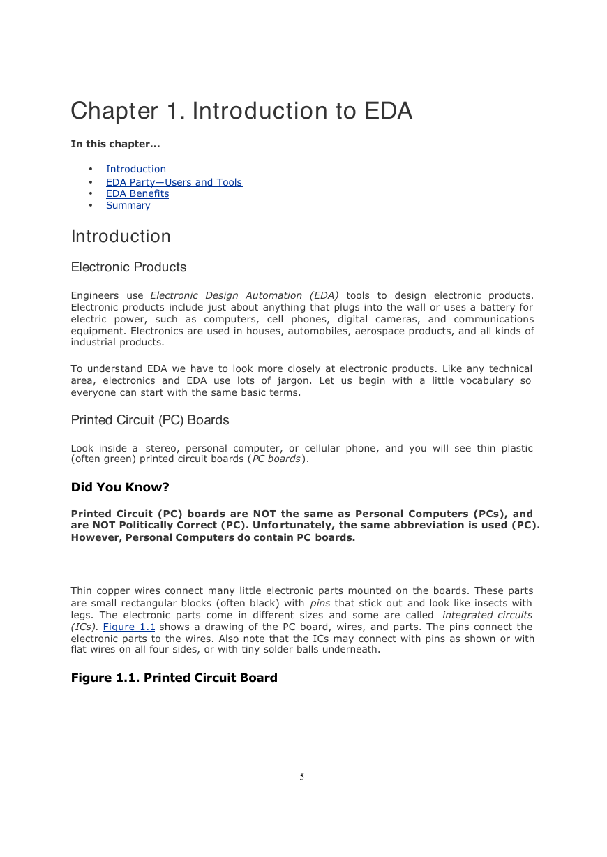
Thin copper wires connect many little electronic parts mounted on the boards. These parts
are small rectangular blocks (often black) with pins that stick out and look like insects with
legs. The electronic parts come in different sizes and some are called integrated circuits
(ICs). Figure 1.1 shows a drawing of the PC board, wires, and parts. The pins connect the
electronic parts to the wires. Also note that the ICs may connect with pins as shown or with
flat wires on all four sides, or with tiny solder balls underneath.
Figure 1.1. Printed Circuit Board
5
�
Note that the PC board wires are printed or deposited, and so are flat, not round. The PC
board also has printed copper fingers or connectors at the edge for electrical connections off
the board.
Integrated Circuits
Integrated circuits (ICs) use printed wiring very similar to that on the PC boards. The
"board," however, is now a thin silicon chip, with much smaller devices and wiring. Both the
devices and the wiring are fabricated in the silicon surface.
Did You Know?
The silicon (silly-con) here is a silver, brittle, metallic substance. It is a major
element in ordinary sand. Do not confuse it with silicone (silly-cone), which is the
rubbery material used in caulking and car waxes.
Semiconductor companies make ICs. These are also called chips, microchips, or silicon chips.
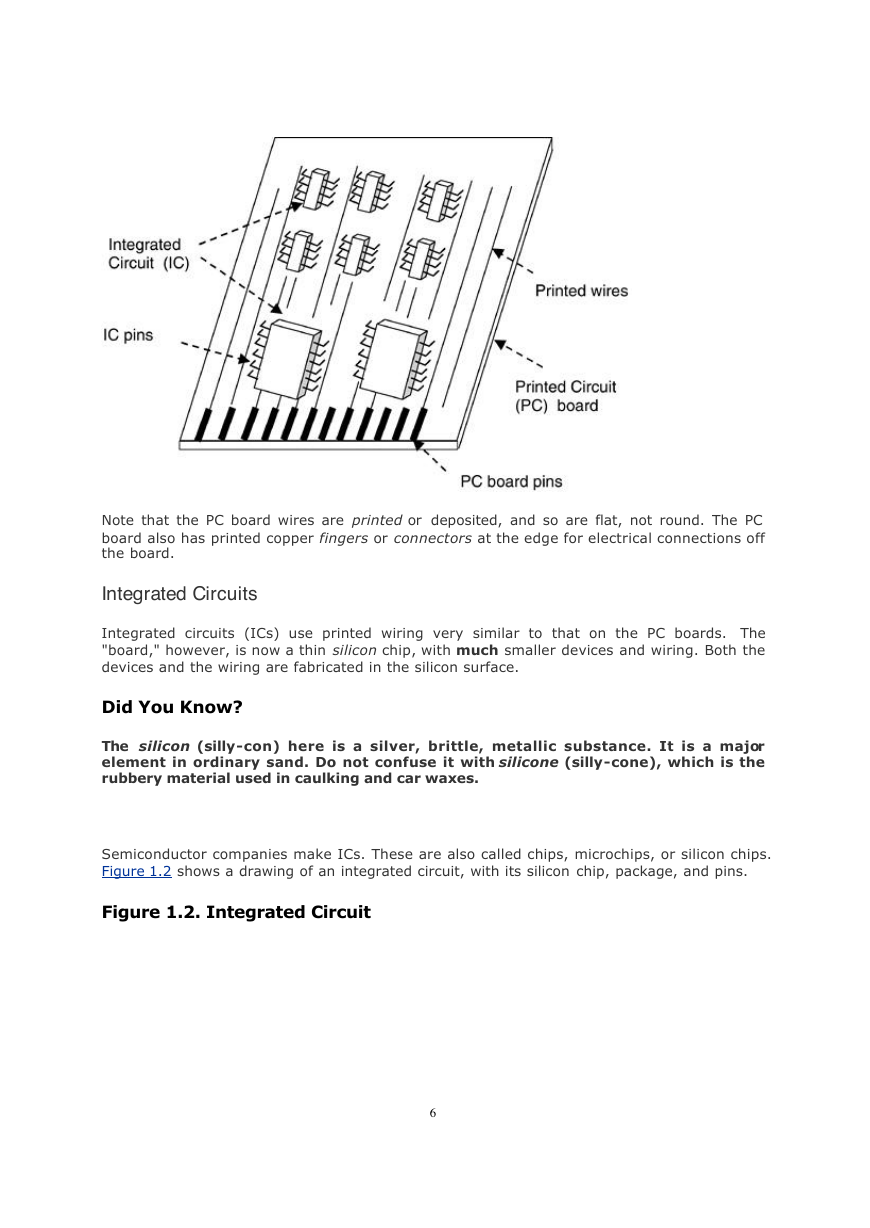
Figure 1.2 shows a drawing of an integrated circuit, with its silicon chip, package, and pins.
Figure 1.2. Integrated Circuit
6
�
The figure shows the fine gold bonding wires which connect the chip pads to the package
pins. The wires are thinner than a human hair. The IC package takes up much more room
than the tiny chip. There are many other styles of IC packages besides the example shown.
Some chips are encased in smaller chip scale packages. Some ICs (called flip chips) can
connect directly to PC boards, without package, wires, or pins. This allows those boards to
hold more chips.
The ICs hold millions of tiny electrical switches called transistors. Thread-like printed wires
on the IC connect transistors (and other devic es) to form electrical circuits. These circuits
are the heart of all electronic products. They can make small electrical signals larger
(amplify) or make logical decisions (e.g., does number A = number B?). Basic logic circuits
are called gates.
CAD, CAM, CAE, and EDA
Arranging the ICs and wire routes on the PC board is called layout. Programmers developed
Computer Aided Design (CAD) software tools to help with the tedious PC board layout.
Engineers later adapted PC board CAD tools for similar use on ICs.
Programmers continued to develop many other software tools to help design the IC and
verify its behavior. Some are called Computer Aided Engineering (CAE). Others are called
Computer Aided Manufacturing (CAM). Electronic Design Automation (EDA) is an umbrella
term for all these tools.
Data, Signals, and Input/Output
The information that is transferred between electronic products and ICs is called data. Data
consists of numbers, letters, voice, video, etc. When electricity is sent from one IC to
another, it is called a signal. Signals going into a product or IC are inputs, and those coming
out are called outputs. Input and output together are referred to as input/output or I/O.
(You can read more about silicon, semiconductors, and computers in Appendices A, B, and
C.)
7
�
Electronic Product Development
Neither the electronic products nor the ICs could be made without the use of EDA tools. EDA
is intimately bound to the semiconductor IC and electronic product design industries.
Engineers use EDA tools to design electronic systems and ICs. To learn about EDA, we have
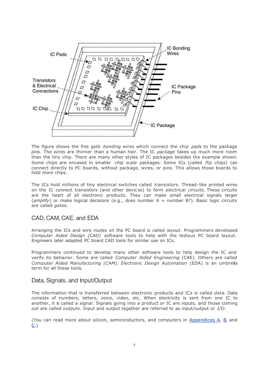
to understand what the engineers are trying to do. Figure 1.3 gives an overall view from
electronic product to IC.
Figure 1.3. Electronic Product Development
In Figure 1.3, we see the system engineers discussing the idea for a new cellular telephone
product. They create a set of IC requirements for the electronics which they need in the
product. The requirements are similar to an architect's drawings.
8
�


 2023年江西萍乡中考道德与法治真题及答案.doc
 2012年重庆南川中考生物真题及答案.doc
 2013年江西师范大学地理学综合及文艺理论基础考研真题.doc
 2020年四川甘孜小升初语文真题及答案I卷.doc
 2020年注册岩土工程师专业基础考试真题及答案.doc
 2023-2024学年福建省厦门市九年级上学期数学月考试题及答案.doc
 2021-2022学年辽宁省沈阳市大东区九年级上学期语文期末试题及答案.doc
 2022-2023学年北京东城区初三第一学期物理期末试卷及答案.doc
 2018上半年江西教师资格初中地理学科知识与教学能力真题及答案.doc
 2012年河北国家公务员申论考试真题及答案-省级.doc
 2020-2021学年江苏省扬州市江都区邵樊片九年级上学期数学第一次质量检测试题及答案.doc
 2022下半年黑龙江教师资格证中学综合素质真题及答案.doc