IC1114-F48LQ
1. FEATURES
− High speed 8-bit micro-controller with 4 system clocks
per machine cycle
Instruction-set compatible with MCS-51
−
− Embedded 32K-byte program FLASH ROM for
product quick delivery. In System Programming, ISP is
supported by either USB or I2C port.
− Built in fixed address 256 bytes data RAM.
− Built in floating address 4608 bytes data RAM
− Extra 1K bytes CPU data RAM space available by
disable central control block function.
− System power saving mode ready, idle & power down
modes.
endpoints. (Including control, interrupt, bulk in and
bulk out endpoints)
− Built in ICSI in-house bi-directional parallel port for
quick data transfer. Both master and slave modes are
supported.
− Master/Slave IIC and UART/RS-232 interface for
external device communication.
− Smart Media Card/NAND type flash chip interface
complies with Smart Media Specification Rev.1.1 and
Smart Media Identify Number Specification Version
1.1
− Built-in hardware ECC (Error Correction Code) check
− Three programmable 16-bit timer/counter and
for Smart Media Card/NAND type flash chip.
watchdog timer.
− Compliant with USB Specification Rev.1.1 supports
full speed (12Mbits/sec), one device address and four
− 3.0~3.6V supply.
− 48LQFP packages is available.
Integrated Circuit Solution Inc.
1
Version 1.0
�
IC1114-F48LQ
2.
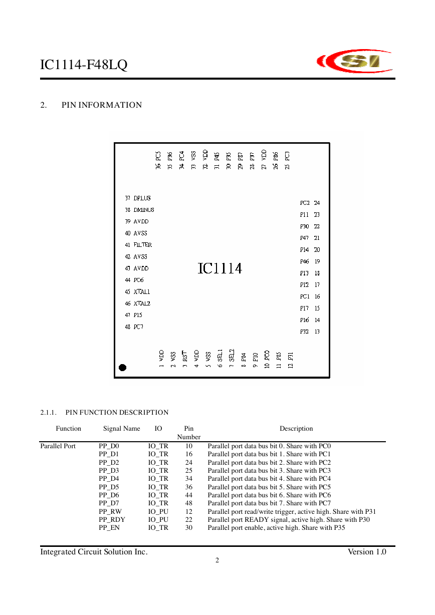
PIN INFORMATION
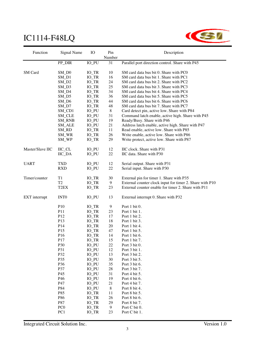
2.1.1. PIN FUNCTION DESCRIPTION
Function
Signal Name
IO
Parallel Port
PP_D0
PP_D1
PP_D2
PP_D3
PP_D4
PP_D5
PP_D6
PP_D7
PP_RW
PP_RDY
PP_EN
IO_TR
IO_TR
IO_TR
IO_TR
IO_TR
IO_TR
IO_TR
IO_TR
IO_PU
IO_PU
IO_TR
Pin
Number
10
16
24
25
34
36
44
48
12
22
30
Description
Parallel port data bus bit 0. Share with PC0
Parallel port data bus bit 1. Share with PC1
Parallel port data bus bit 2. Share with PC2
Parallel port data bus bit 3. Share with PC3
Parallel port data bus bit 4. Share with PC4
Parallel port data bus bit 5. Share with PC5
Parallel port data bus bit 6. Share with PC6
Parallel port data bus bit 7. Share with PC7
Parallel port read/write trigger, active high. Share with P31
Parallel port READY signal, active high. Share with P30
Parallel port enable, active high. Share with P35
Integrated Circuit Solution Inc.
2
Version 1.0
�
IC1114-F48LQ
Function
SM Card
Master/Slave IIC
UART
Timer/counter
EXT interrupt
Signal Name
IO
PP_DIR
SM_D0
SM_D1
SM_D2
SM_D3
SM_D4
SM_D5
SM_D6
SM_D7
SM_CD1
SM_CLE
SM_RNB
SM_ALE
SM_RD
SM_WR
SM_WP
IIC_CL
IIC_DA
TXD
RXD
T1
T2
T2EX
INT0
P10
P11
P12
P13
P14
P15
P16
P17
P30
P31
P32
P35
P36
P37
P45
P46
P47
P84
P85
P86
P87
PC0
PC1
IO_PU
IO_TR
IO_TR
IO_TR
IO_TR
IO_TR
IO_TR
IO_TR
IO_TR
IO_PU
IO_PU
IO_PU
IO_PU
IO_TR
IO_TR
IO_TR
IO_PU
IO_PU
IO_PU
IO_PU
IO_TR
IO_TR
IO_TR
IO_PU
IO_TR
IO_TR
IO_TR
IO_TR
IO_TR
IO_TR
IO_TR
IO_TR
IO_PU
IO_PU
IO_PU
IO_PU
IO_PU
IO_PU
IO_PU
IO_PU
IO_PU
IO_PU
IO_TR
IO_TR
IO_TR
IO_TR
IO_TR
Description
Parallel port direction control. Share with P45
SM card data bus bit 0. Share with PC0
SM card data bus bit 1. Share with PC1
SM card data bus bit 2. Share with PC2
SM card data bus bit 3. Share with PC3
SM card data bus bit 4. Share with PC4
SM card data bus bit 5. Share with PC5
SM card data bus bit 6. Share with PC6
SM card data bus bit 7. Share with PC7
Card detect pin, active low. Share with P84
Command latch enable, active high. Share with P45
Ready/Busy. Share with P46
Address latch enable, active high. Share with P47
Read enable, active low. Share with P85
Write enable, active low. Share with P86
Write protect, active low. Share with P87
IIC clock. Share with P31
IIC data. Share with P30
Serial output. Share with P31
Serial input. Share with P30
External pin for timer 1. Share with P35
External counter clock input for timer 2. Share with P10
External counter enable for timer 2. Share with P11
External interrupt 0. Share with P32
Port 1 bit 0.
Port 1 bit 1.
Port 1 bit 2.
Port 1 bit 3.
Port 1 bit 4.
Port 1 bit 5.
Port 1 bit 6.
Port 1 bit 7.
Port 3 bit 0.
Port 3 bit 1.
Port 3 bit 2.
Port 3 bit 5.
Port 3 bit 6.
Port 3 bit 7.
Port 4 bit 5.
Port 4 bit 6.
Port 4 bit 7.
Port 8 bit 4.
Port 8 bit 5.
Port 8 bit 6.
Port 8 bit 7.
Port C bit 0.
Port C bit 1.
Pin
Number
31
10
16
24
25
34
36
44
48
8
31
19
21
11
26
29
12
22
12
22
30
9
23
13
9
23
17
18
20
47
14
15
22
12
13
30
35
28
31
19
21
8
11
26
29
9
23
Integrated Circuit Solution Inc.
3
Version 1.0
�
Description
Port C bit 2.
Port C bit 3.
Port C bit 4.
Port C bit 5.
Port C bit 6.
Port C bit 7.
External loop filter pin, a capacitor is connected between this
pin and analog ground
USB DPLUS pin
USB DMINUS pin
XTAL oscillator input pin
XTAL oscillator output pin
Pin
Number
17
18
20
47
14
15
41
37
38
45
46
3
6
7
IC1114-F48LQ
Function
Signal Name
IO
PLL
PC2
PC3
PC4
PC5
PC6
PC7
FILTER
IO_TR
IO_TR
IO_TR
IO_TR
IO_TR
IO_TR
O
DPLUS
DMINUS
XTAL1
XTAL2
AVDD
AVSS
VSS
VDD
RST
SEL1
SEL2
USB
XTAL
Power
Power
SELCLK
Note :
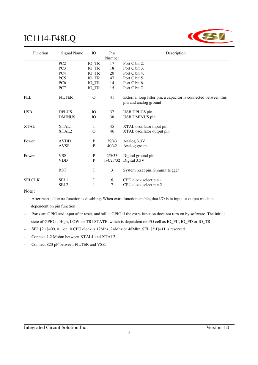
− After reset, all extra function is disabling. When extra function enable, that I/O is in input or output mode is
System reset pin, Shmmit trigger
CPU clock select pin 1
CPU clock select pin 2
2/5/33 Digital ground pin
1/4/27/32 Digital 3.3V
IO
IO
I
O
P
P
P
P
I
I
I
39/43 Analog 3.3V
40/42 Analog ground
dependent on pin function.
− Ports are GPIO and input after reset, and still a GPIO if the extra function does not turn on by software. The initial
state of GPIO is High, LOW, or TRI-STATE, which is dependent on I/O cell as IO_PU, IO_PD or IO_TR.
− SEL [2:1]=00, 01, or 10 CPU clock is 12Mhz, 24Mhz or 48Mhz. SEL [2:1]=11 is reserved.
− Connect 1.2 Mohm between XTAL1 and XTAL2.
− Connect 820 pF between FILTER and VSS.
Integrated Circuit Solution Inc.
4
Version 1.0
�
IC1114-F48LQ
3. FUNCTION DESCRIPTION
IC1114 includes a turbo 80T32 CPU core, 32K-byte internal program Flash-ROM, 5.5-bytes SRAM and many
interface blocks. Including USB function, SM flash card interface, UART, NAND type flash chip interface,
I2C master & slave blocks and high speed parallel port master & slave interface.
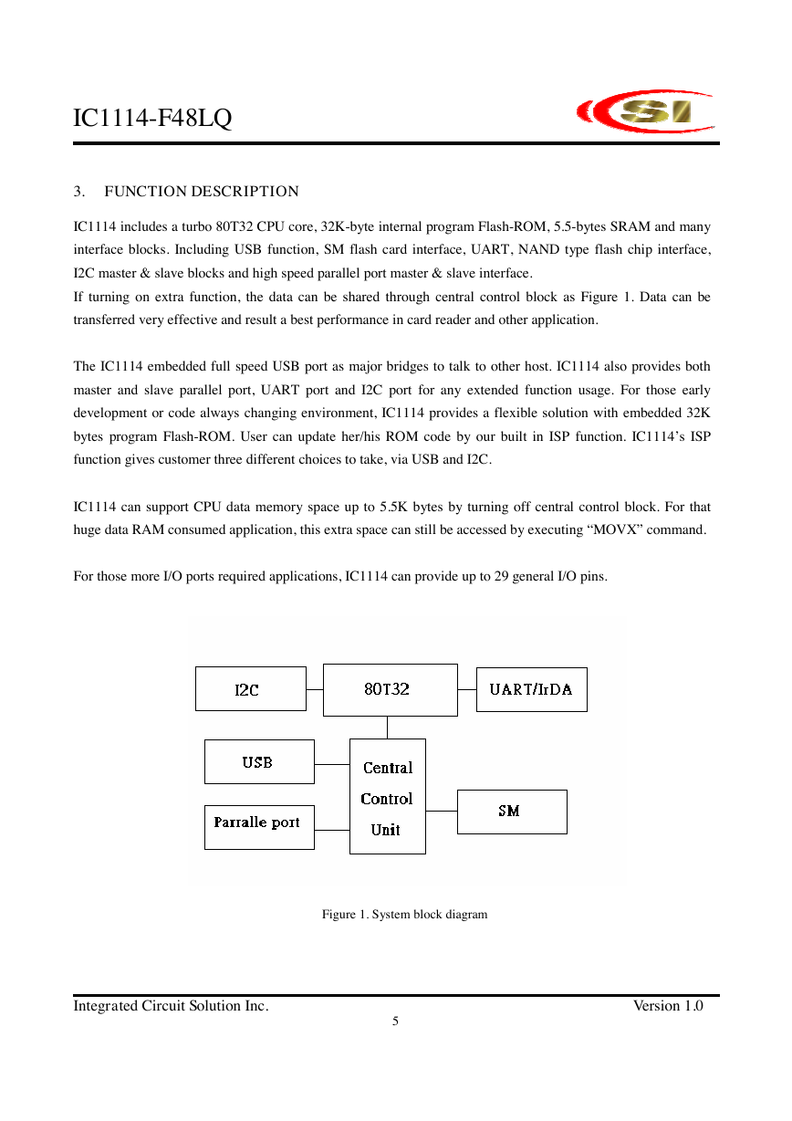
If turning on extra function, the data can be shared through central control block as Figure 1. Data can be
transferred very effective and result a best performance in card reader and other application.
The IC1114 embedded full speed USB port as major bridges to talk to other host. IC1114 also provides both
master and slave parallel port, UART port and I2C port for any extended function usage. For those early
development or code always changing environment, IC1114 provides a flexible solution with embedded 32K
bytes program Flash-ROM. User can update her/his ROM code by our built in ISP function. IC1114’s ISP
function gives customer three different choices to take, via USB and I2C.
IC1114 can support CPU data memory space up to 5.5K bytes by turning off central control block. For that
huge data RAM consumed application, this extra space can still be accessed by executing “MOVX” command.
For those more I/O ports required applications, IC1114 can provide up to 29 general I/O pins.
Figure 1. System block diagram
Integrated Circuit Solution Inc.
5
Version 1.0
�
IC1114-F48LQ
4. ABSOLUTE MAXIMUM RATINGS
Parameter
Operating temperature under bias
Storage temperature range
Voltage on I/O port
Voltage on any other pin to VSS
Rating
0 to +70
-65 to +125
5.5
3.8
Unit
℃
℃
V
V
Stressing the device beyond the "Absolute Maximum Rating" may cause permanent damage. This is stress
rating only. Operation beyond the "operating conditions" is not recommended and extended exposure beyond
the "operating conditions" may affect device reliability.
OPERATING RANGES
Commercial devices case temperature
VCC supply voltage
Input capacitor
Input Voltage of I/O port
Input Voltage of other pin
Oscillator frequency
0 to +70 ℃
+3.0 to 3.6V
5 pF
Vss-0.3, 5.5V
Vss-0.3, VDD+0.3
12 MHz
Minimum D.C. input voltage is -0.5 V. During transitions, inputs may undershoot ,to -2.0 V for periods less
than 20 ns. Maximum D.C. voltage on output pins is VCC+0.5 V, which may overshoot to VCC + 2.0 V for
periods less than 20 ns.
Integrated Circuit Solution Inc.
6
Version 1.0
�
IC1114-F48LQ
5. DC ELECTRICAL CHARACTERISTICS
(VDD-VSS= 3.6V to 3.0V)
Symbol
Vil
Vih
Vil1
Input low voltage of GPIO
Input high voltage of GPIO
Input low voltage (XTAL1)
Parameter
Min
-0.5
2.0
-0.5
Input high voltage (XTAL1)
Vih1
Vsch+ RST positive Schmidt-trigger threshold voltage
Vsch- RST negative Schmidt-trigger threshold voltage
Vol
Output low voltage of USB
Max Unit Test conditions
0.8
5.5
0.2Vcc
- 0.3
V
V Vcc=3.0V
V
0.7Vcc Vcc+0.5 V
Vcc+0.5 V
V
V Iol=4.0mA,
Vcc=3.0V
2.0
0
0.8
0.4
2.4
V Ioh=4.0mA,
V
V
Vcc=3.0V
Iol=4.0mA,
Vcc=3.0V
Ioh=4.0mA
Vcc=3.0V
Vcc=3.6V, no load
uA Vin=0Vor 3.6V
ohm
mA
mA
mA
mA
mA
mA
uA Vcc=3.6V
V
Vcc=3.6V, no load
Voh
Vol
Output high voltage of USB
Output low voltage of I/O port, RST
Voh
Output high voltage of I/O port, RST
Ili
Ru
Icc
active
mode
Icci idle
mode
Input leakage current
IO_PU pull up resister
12 MHz
24 MHz
48 MHz
12 MHz
24 MHz
48 MHz
Current in power down mode
Minimum voltage to keep RAM data
Ipd
Vdr
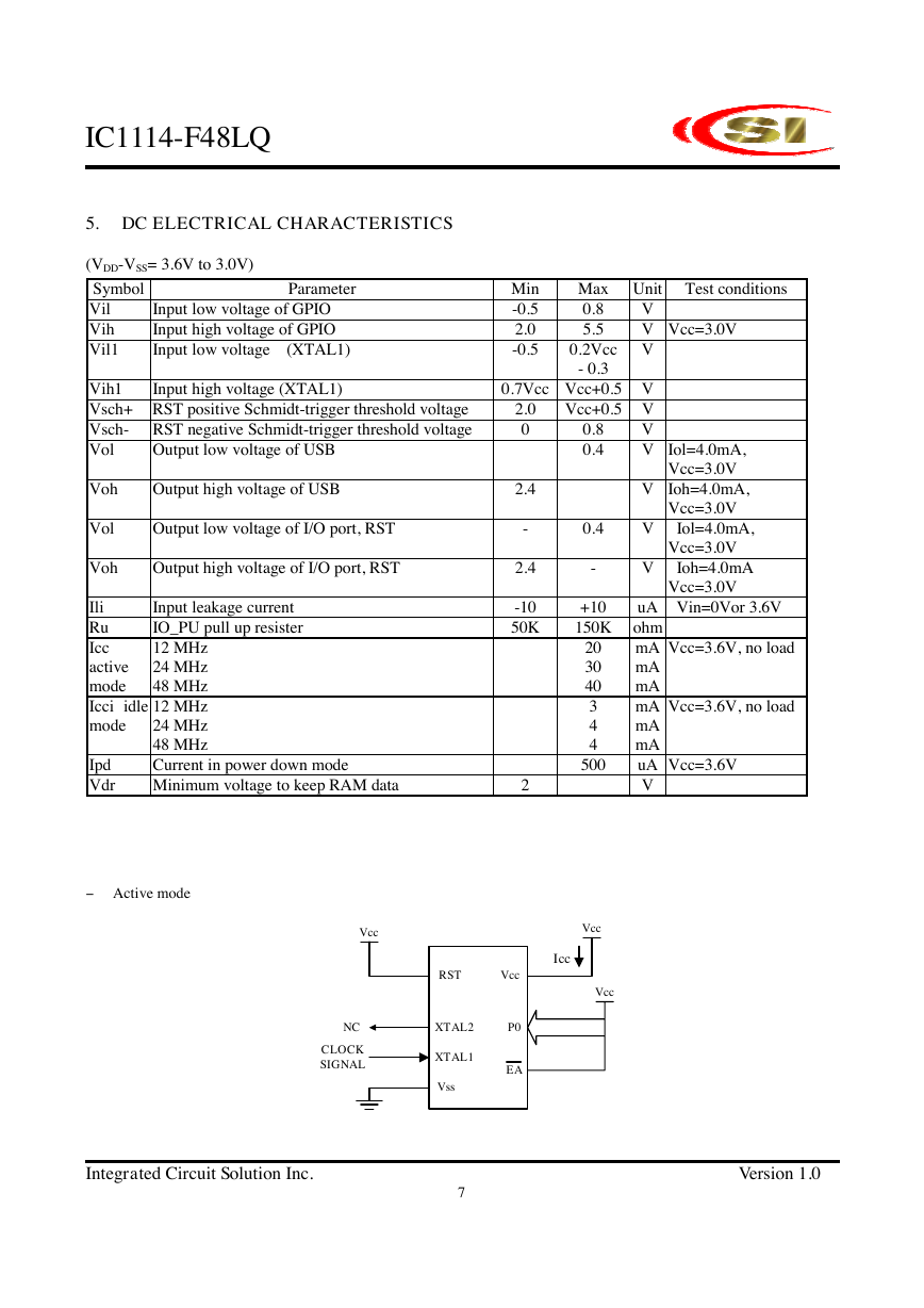
− Active mode
Vcc
NC
CLOCK
SIGNAL
Integrated Circuit Solution Inc.
-
2.4
-10
50K
2
0.4
-
+10
150K
20
30
40
3
4
4
500
Vcc
Icc
Vcc
RST
Vcc
XTAL2
XTAL1
Vss
P0
EA
7
Version 1.0
�
Vcc
Icc
Vcc
IC1114-F48LQ
−
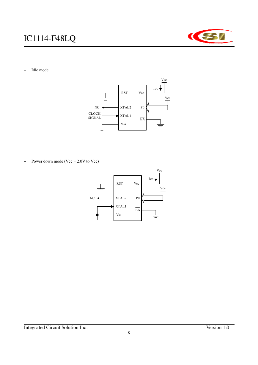
Idle mode
NC
CLOCK
SIGNAL
RST
Vcc
P0
EA
XTAL2
XTAL1
Vss
− Power down mode (Vcc = 2.0V to Vcc)
Vcc
Icc
Vcc
NC
RST
Vcc
XTAL2
XTAL1
Vss
P0
EA
Integrated Circuit Solution Inc.
8
Version 1.0
�



 2023年江西萍乡中考道德与法治真题及答案.doc
 2012年重庆南川中考生物真题及答案.doc
 2013年江西师范大学地理学综合及文艺理论基础考研真题.doc
 2020年四川甘孜小升初语文真题及答案I卷.doc
 2020年注册岩土工程师专业基础考试真题及答案.doc
 2023-2024学年福建省厦门市九年级上学期数学月考试题及答案.doc
 2021-2022学年辽宁省沈阳市大东区九年级上学期语文期末试题及答案.doc
 2022-2023学年北京东城区初三第一学期物理期末试卷及答案.doc
 2018上半年江西教师资格初中地理学科知识与教学能力真题及答案.doc
 2012年河北国家公务员申论考试真题及答案-省级.doc
 2020-2021学年江苏省扬州市江都区邵樊片九年级上学期数学第一次质量检测试题及答案.doc
 2022下半年黑龙江教师资格证中学综合素质真题及答案.doc