www.ti.com
5-A, WIDE INPUT RANGE, STEP-DOWN SWIFT™ CONVERTER
TPS5450
SLVS757–MARCH 2007
1FEATURES
2• Wide Input Voltage Range: 5.5 V to 36 V
• Up to 5-A Continuous (6-A Peak) Output
Current
• High Efficiency Greater than 90% Enabled by
110-mΩ Integrated MOSFET Switch
• Wide Output Voltage Range: Adjustable Down
•
to 1.22 V with 1.5% Initial Accuracy
Internal Compensation Minimizes External
Parts Count
• Fixed 500 kHz Switching Frequency for Small
Filter Size
• 18 μA Shut Down Supply Current
•
Improved Line Regulation and Transient
Response by Input Voltage Feed Forward
• System Protected by Overcurrent Limiting,
Overvoltage Protection and Thermal Shutdown
• –40 C to 125 C Operating Junction
Temperature Range
• Available in Small Thermally Enhanced 8-Pin
SOIC PowerPAD™ Package
• For SWIFT™ Documentation, Application
Notes and Design Software, See the TI Website
at www.ti.com/swift
APPLICATIONS
• High Density Point-of-Load Regulators
• LCD Displays, Plasma Displays
• Battery Chargers
• 12-V/24-V Distributed Power Systems
DESCRIPTION
As a member of
the SWIFT™ family of DC/DC
regulators,
the TPS5450 is a high-output-current
PWM converter that integrates a low resistance high
side N-channel MOSFET. Included on the substrate
with the listed features are a high performance
voltage error amplifier
that provides tight voltage
regulation accuracy under transient conditions; an
undervoltage-lockout circuit to prevent start-up until
the input voltage reaches 5.5 V; an internally set
slow-start circuit to limit inrush currents; and a voltage
feed-forward
transient
response. Using the ENA pin, shutdown supply
current is reduced to 18 μA typically. Other features
include an active-high enable, overcurrent
limiting,
overvoltage protection and thermal shutdown. To
reduce design complexity and external component
count,
the TPS5450 feedback loop is internally
compensated.
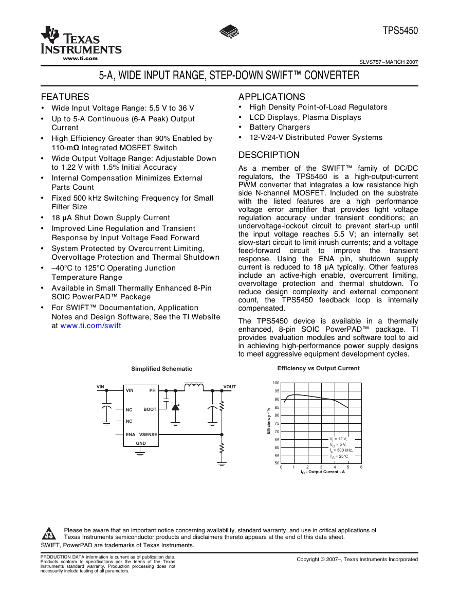
The TPS5450 device is available in a thermally
enhanced, 8-pin SOIC PowerPAD™ package. TI
provides evaluation modules and software tool to aid
in achieving high-performance power supply designs
to meet aggressive equipment development cycles.
improve
the
circuit
to
1
Please be aware that an important notice concerning availability, standard warranty, and use in critical applications of
Texas Instruments semiconductor products and disclaimers thereto appears at the end of this data sheet.
2SWIFT, PowerPAD are trademarks of Texas Instruments.
PRODUCTION DATA information is current as of publication date.
Products conform to specifications per the terms of
the Texas
Instruments standard warranty. Production processing does not
necessarily include testing of all parameters.
Copyright © 2007–, Texas Instruments Incorporated
VINNCNCENAGNDVSENSEBOOTPHVINVOUTSimplified SchematicEfficiency vs Output Current50556065707580859095100I-OutputCurrent-AOEfficiency - %0123456V= 12 V,V= 5 V,f= 500 kHz,T= 25°CIOsA�
TPS5450
SLVS757–MARCH 2007
These devices have limited built-in ESD protection. The leads should be shorted together or the device placed in conductive foam
during storage or handling to prevent electrostatic damage to the MOS gates.
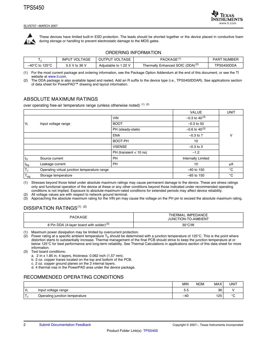
TJ
–40 C to 125 C
INPUT VOLTAGE
5.5 V to 36 V
OUTPUT VOLTAGE
Adjustable to 1.22 V
PACKAGE(1)
Thermally Enhanced SOIC (DDA)(2)
PART NUMBER
TPS5450DDA
ORDERING INFORMATION
(1) For the most current package and ordering information, see the Package Option Addendum at the end of this document, or see the TI
website at www.ti.com.
(2) The DDA package is also available taped and reeled. Add an R suffix to the device type (i.e., TPS5450DDAR). See applications section
of data sheet for PowerPAD™ drawing and layout information.
ABSOLUTE MAXIMUM RATINGS
over operating free-air temperature range (unless otherwise noted) (1) (2)
VI
Input voltage range
VIN
BOOT
PH (steady-state)
ENA
BOOT-PH
VSENSE
PH (transient < 10 ns)
PH
PH
UNIT
V
VALUE
–0.3 to 40(3)
–0.3 to 50
–0.6 to 40(3)
–0.3 to 7
10
–0.3 to 3
–1.2
Source current
Leakage current
Operating virtual junction temperature range
Storage temperature
IO
Ilkg
TJ
Tstg
(1) Stresses beyond those listed under absolute maximum ratings may cause permanent damage to the device. These are stress ratings
–40 to 150
–65 to 150
μA
C
C
Internally Limited
10
only and functional operation of the device at these or any other conditions beyond those indicated under recommended operating
conditions is not implied. Exposure to absolute-maximum-rated conditions for extended periods may affect device reliability.
(2) All voltage values are with respect to network ground terminal.
(3) Approaching the absolute maximum rating for the VIN pin may cause the voltage on the PH pin to exceed the absolute maximum rating.
DISSIPATION RATINGS(1) (2)
PACKAGE
8 Pin DDA (4-layer board with solder)(3)
THERMAL IMPEDANCE
JUNCTION-TO-AMBIENT
30 C/W
(1) Maximum power dissipation may be limited by overcurrent protection.
(2) Power rating at a specific ambient temperature TA should be determined with a junction temperature of 125 C. This is the point where
distortion starts to substantially increase. Thermal management of the final PCB should strive to keep the junction temperature at or
below 125 C for best performance and long-term reliability. See Thermal Calculations in applications section of this data sheet for more
information.
(3) Test board conditions:
a. 2 in x 1.85 in, 4 layers, thickness: 0.062 inch (1,57 mm).
b. 2 oz. copper traces located on the top and bottom of the PCB.
c. 2 oz. copper ground planes on the 2 internal layers.
d. 4 thermal vias in the PowerPAD area under the device package.
RECOMMENDED OPERATING CONDITIONS
VI
TJ
Input voltage range
Operating junction temperature
NOM
MIN
5.5
–40
MAX
36
125
UNIT
V
C
2
Submit Documentation Feedback
Copyright © 2007–, Texas Instruments Incorporated
Product Folder Link(s): TPS5450
www.ti.com�
ELECTRICAL CHARACTERISTICS
TJ = –40 C to 125 C, VIN = 5.5 V - 36 V (unless otherwise noted)
TPS5450
SLVS757–MARCH 2007
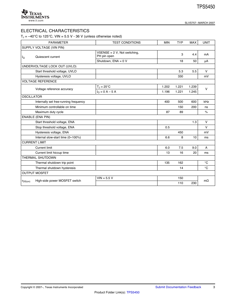
PARAMETER
SUPPLY VOLTAGE (VIN PIN)
IQ
Quiescent current
UNDERVOLTAGE LOCK OUT (UVLO)
Start threshold voltage, UVLO
Hysteresis voltage, UVLO
VOLTAGE REFERENCE
Voltage reference accuracy
OSCILLATOR
Internally set free-running frequency
Minimum controllable on time
Maximum duty cycle
ENABLE (ENA PIN)
Start threshold voltage, ENA
Stop threshold voltage, ENA
Hysteresis voltage, ENA
Internal slow-start time (0~100%)
CURRENT LIMIT
Current limit
Current limit hiccup time
THERMAL SHUTDOWN
Thermal shutdown trip point
Thermal shutdown hysteresis
OUTPUT MOSFET
rDS(on)
High-side power MOSFET switch
VIN = 5.5 V
TEST CONDITIONS
MIN
TYP
MAX
UNIT
VSENSE = 2 V, Not switching,
PH pin open
Shutdown, ENA = 0 V
4.4
50
5.5
3
18
5.3
330
TJ = 25 C
IO = 0 A – 5 A
1.202
1.196
1.221
1.221
1.239
1.245
mA
μA
V
mV
V
kHz
ns
%
V
V
mV
ms
A
ms
C
C
mΩ
400
87
0.5
6.6
6.0
13
135
500
150
89
450
8
7.5
16
162
14
150
110
600
200
1.3
10
9.0
20
230
Copyright © 2007–, Texas Instruments Incorporated
Submit Documentation Feedback
3
Product Folder Link(s): TPS5450
www.ti.com�
TPS5450
SLVS757–MARCH 2007
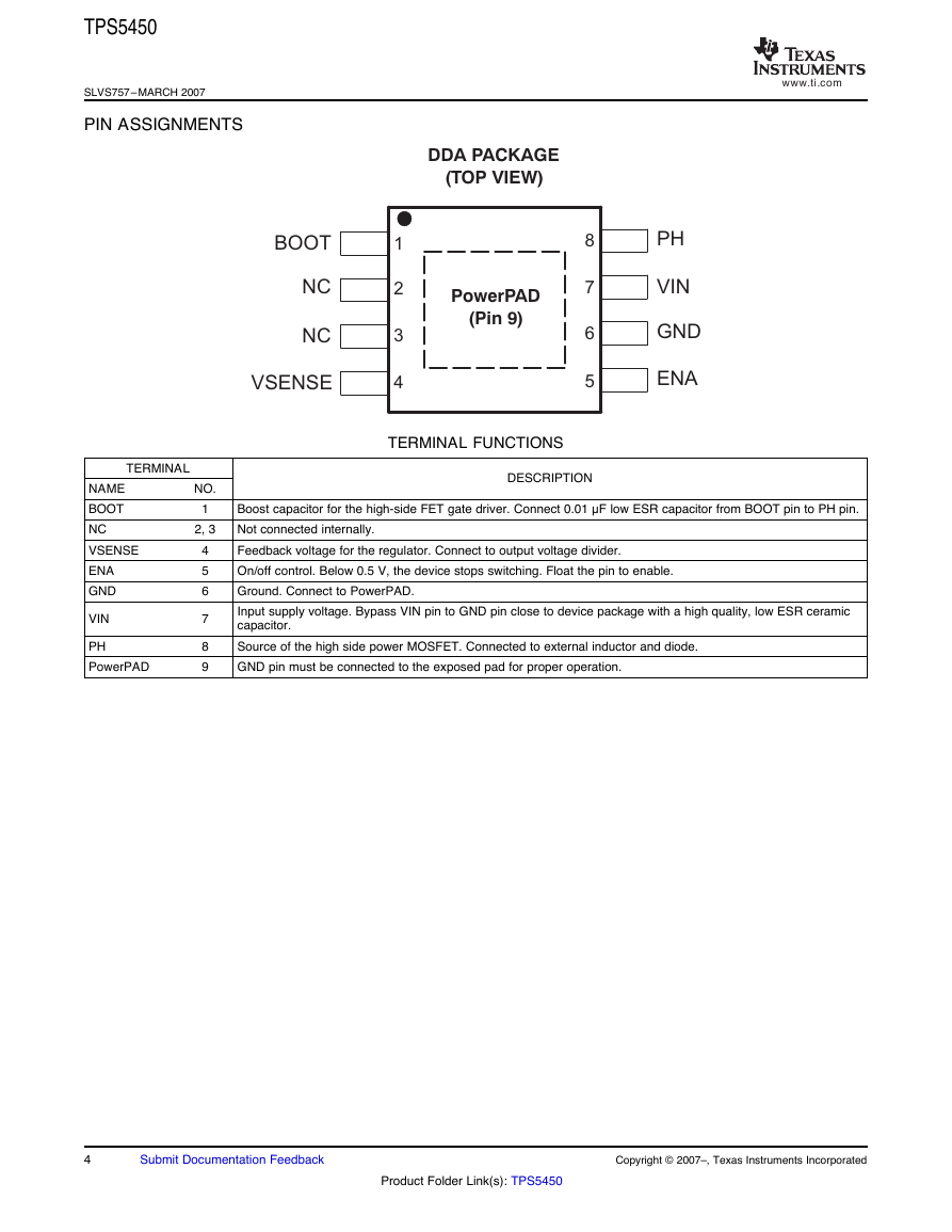
PIN ASSIGNMENTS
TERMINAL
NAME
BOOT
NC
VSENSE
ENA
GND
VIN
PH
PowerPAD
NO.
1
2, 3
4
5
6
7
8
9
TERMINAL FUNCTIONS
DESCRIPTION
Boost capacitor for the high-side FET gate driver. Connect 0.01 μF low ESR capacitor from BOOT pin to PH pin.
Not connected internally.
Feedback voltage for the regulator. Connect to output voltage divider.
On/off control. Below 0.5 V, the device stops switching. Float the pin to enable.
Ground. Connect to PowerPAD.
Input supply voltage. Bypass VIN pin to GND pin close to device package with a high quality, low ESR ceramic
capacitor.
Source of the high side power MOSFET. Connected to external inductor and diode.
GND pin must be connected to the exposed pad for proper operation.
4
Submit Documentation Feedback
Copyright © 2007–, Texas Instruments Incorporated
Product Folder Link(s): TPS5450
www.ti.com12348765PowerPAD(Pin 9)BOOTNCNCVSENSEPHVINGNDENADDA PACKAGE(TOP VIEW)�
TPS5450
SLVS757–MARCH 2007
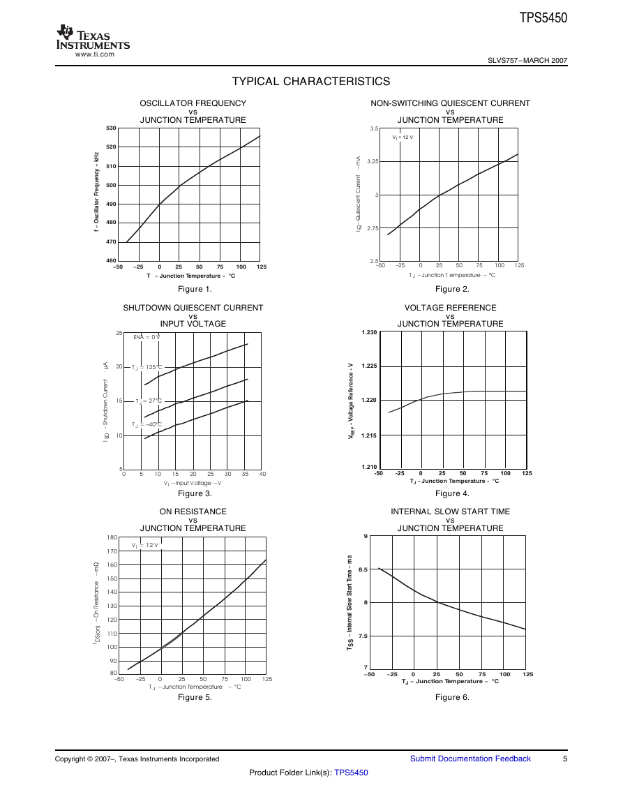
TYPICAL CHARACTERISTICS
OSCILLATOR FREQUENCY
JUNCTION TEMPERATURE
vs
NON-SWITCHING QUIESCENT CURRENT
vs
JUNCTION TEMPERATURE
Figure 1.
Figure 2.
SHUTDOWN QUIESCENT CURRENT
vs
INPUT VOLTAGE
VOLTAGE REFERENCE
vs
JUNCTION TEMPERATURE
Figure 3.
Figure 4.
ON RESISTANCE
vs
JUNCTION TEMPERATURE
INTERNAL SLOW START TIME
JUNCTION TEMPERATURE
vs
Figure 5.
Figure 6.
Copyright © 2007–, Texas Instruments Incorporated
Submit Documentation Feedback
5
Product Folder Link(s): TPS5450
www.ti.com2.52.7533.253.5−50−250255075100125TJ−Junction Temperature−°CIQ−Quiescent Current−mAV= 12 VI460470480490500510520530−50−250255075100125f−Oscillator Frequency−kHzT−Junction Temperature−°C1.2101.2151.2201.2251.230-50-250255075100125T- Junction Temperature - °CJV- Voltage Reference - VREF5101520250510152025303540TJ= 125°CTJ= 27°CTJ=–°40CENA = 0 VVI−Input Voltage−VISD−Shutdown Current−Aµ77.588.59−50−250255075100125TJ−Junction Temperature−°CTSS−Internal Slow Start Time−ms8090100110120130140150160170180−50−250255075100125mΩ−On Resistance−rDS(on)TJ−Junction Temperature−°CVI= 12 V�
TPS5450
SLVS757–MARCH 2007
TYPICAL CHARACTERISTICS (continued)
MINIMUM CONTROLLABLE ON TIME
vs
JUNCTION TEMPERATURE
MINIMUM CONTROLLABLE DUTY RATIO
vs
JUNCTION TEMPERATURE
Figure 7.
Figure 8.
6
Submit Documentation Feedback
Copyright © 2007–, Texas Instruments Incorporated
Product Folder Link(s): TPS5450
www.ti.com77.257.507.758-50-250255075100125T- Junction Temperature - °CJMinimum Duty Ratio - %120130140150160170180−50−250255075100125TJ−Junction Temperature−°CMinimum Controllable On Time−ns�
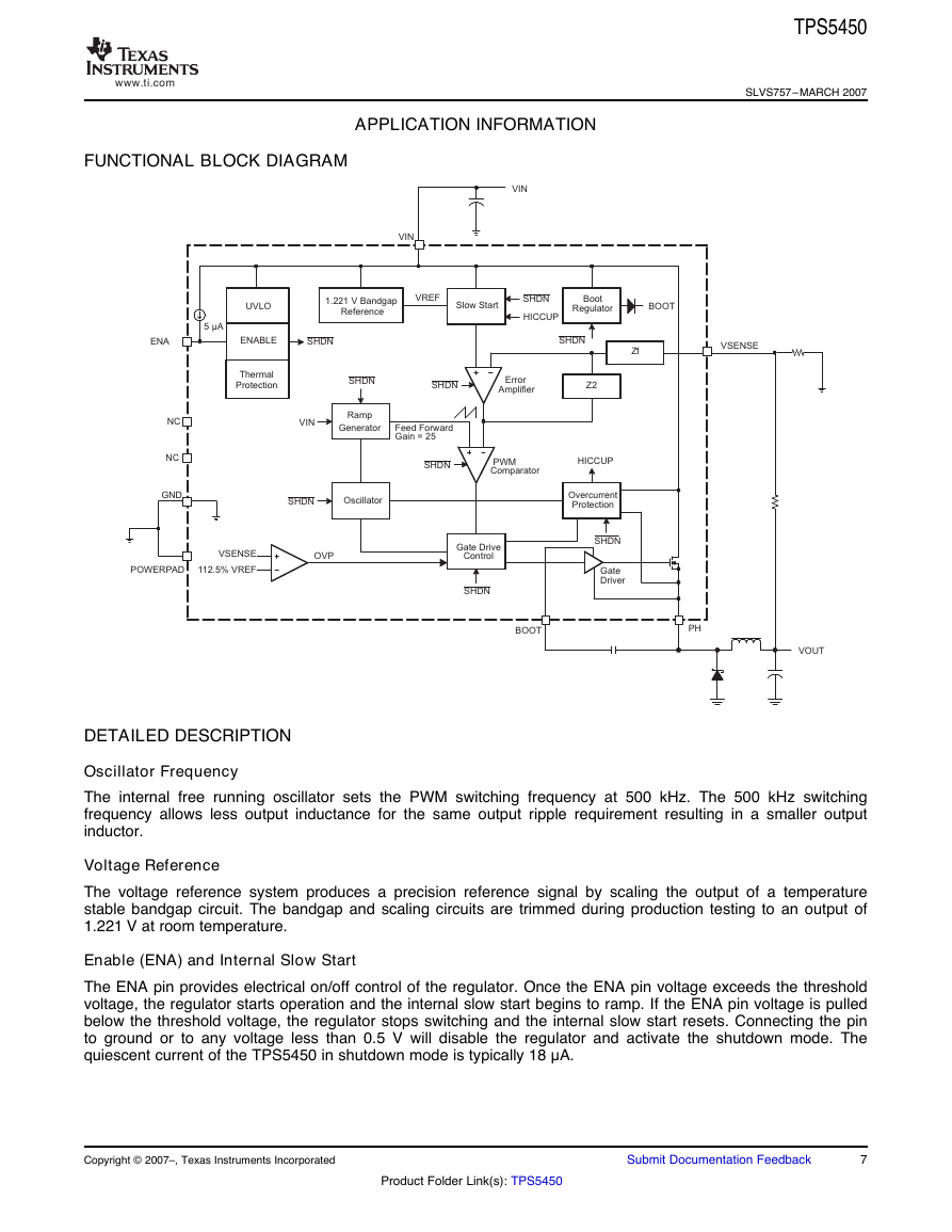
FUNCTIONAL BLOCK DIAGRAM
APPLICATION INFORMATION
TPS5450
SLVS757–MARCH 2007
DETAILED DESCRIPTION
Oscillator Frequency
The internal free running oscillator sets the PWM switching frequency at 500 kHz. The 500 kHz switching
frequency allows less output inductance for the same output ripple requirement resulting in a smaller output
inductor.
Voltage Reference
The voltage reference system produces a precision reference signal by scaling the output of a temperature
stable bandgap circuit. The bandgap and scaling circuits are trimmed during production testing to an output of
1.221 V at room temperature.
Enable (ENA) and Internal Slow Start
The ENA pin provides electrical on/off control of the regulator. Once the ENA pin voltage exceeds the threshold
voltage, the regulator starts operation and the internal slow start begins to ramp. If the ENA pin voltage is pulled
below the threshold voltage, the regulator stops switching and the internal slow start resets. Connecting the pin
to ground or to any voltage less than 0.5 V will disable the regulator and activate the shutdown mode. The
quiescent current of the TPS5450 in shutdown mode is typically 18 μA.
Copyright © 2007–, Texas Instruments Incorporated
Submit Documentation Feedback
7
Product Folder Link(s): TPS5450
www.ti.comVINUVLOENABLEThermalProtectionReferenceOvercurrentGate DriveOscillatorRampGeneratorVREFPHENAGNDBOOTZ1Z2SHDNSHDNSHDNSHDNSHDNSHDNSHDNSHDNVIN112.5% VREFVSENSEOVPHICCUPHICCUPSHDNNCFeed ForwardBOOTNCPOWERPADVINVOUT5µA1.221 V BandgapSlow StartBootRegulatorErrorAmplifierGain = 25PWMComparatorProtectionGateDriverControlVSENSE�
TPS5450
SLVS757–MARCH 2007
The ENA pin has an internal pullup current source, allowing the user to float the ENA pin. If an application
requires controlling the ENA pin, use open drain or open collector output logic to interface with the pin. To limit
the start-up inrush current, an internal slow-start circuit is used to ramp up the reference voltage from 0 V to its
final value, linearly. The internal slow start time is 8 ms typically.
Undervoltage Lockout (UVLO)
The TPS5450 incorporates an undervoltage lockout circuit to keep the device disabled when VIN (the input
voltage) is below the UVLO start voltage threshold. During power up, internal circuits are held inactive and the
internal slow start is grounded until VIN exceeds the UVLO start
threshold voltage. Once the UVLO start
threshold voltage is reached, the internal slow start is released and device start-up begins. The device operates
until VIN falls below the UVLO stop threshold voltage. The typical hysteresis in the UVLO comparator is 330 mV.
Boost Capacitor (BOOT)
Connect a 0.01 μF low-ESR ceramic capacitor between the BOOT pin and PH pin. This capacitor provides the
gate drive voltage for the high-side MOSFET. X7R or X5R grade dielectrics are recommended due to their stable
values over temperature.
Output Feedback (VSENSE) and Internal Compensation
The output voltage of the regulator is set by feeding back the center point voltage of an external resistor divider
network to the VSENSE pin. In steady-state operation, the VSENSE pin voltage should be equal to the voltage
reference 1.221 V.
The TPS5450 implements internal compensation to simplify the regulator design. Since the TPS5450 uses
voltage mode control, a type 3 compensation network has been designed on chip to provide a high crossover
frequency and a high phase margin for good stability. See the Internal Compensation Network in the applications
section for more details.
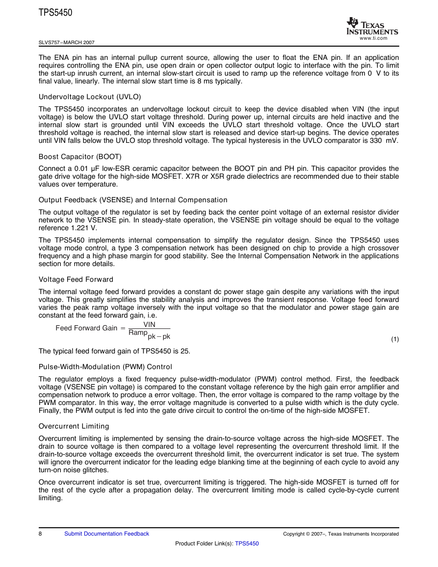
Voltage Feed Forward
The internal voltage feed forward provides a constant dc power stage gain despite any variations with the input
voltage. This greatly simplifies the stability analysis and improves the transient response. Voltage feed forward
varies the peak ramp voltage inversely with the input voltage so that the modulator and power stage gain are
constant at the feed forward gain, i.e.
(1)
The typical feed forward gain of TPS5450 is 25.
Pulse-Width-Modulation (PWM) Control
the feedback
The regulator employs a fixed frequency pulse-width-modulator (PWM) control method. First,
voltage (VSENSE pin voltage) is compared to the constant voltage reference by the high gain error amplifier and
compensation network to produce a error voltage. Then, the error voltage is compared to the ramp voltage by the
PWM comparator. In this way, the error voltage magnitude is converted to a pulse width which is the duty cycle.
Finally, the PWM output is fed into the gate drive circuit to control the on-time of the high-side MOSFET.
Overcurrent Limiting
Overcurrent limiting is implemented by sensing the drain-to-source voltage across the high-side MOSFET. The
drain to source voltage is then compared to a voltage level representing the overcurrent threshold limit. If the
drain-to-source voltage exceeds the overcurrent threshold limit, the overcurrent indicator is set true. The system
will ignore the overcurrent indicator for the leading edge blanking time at the beginning of each cycle to avoid any
turn-on noise glitches.
Once overcurrent indicator is set true, overcurrent limiting is triggered. The high-side MOSFET is turned off for
the rest of the cycle after a propagation delay. The overcurrent limiting mode is called cycle-by-cycle current
limiting.
8
Submit Documentation Feedback
Copyright © 2007–, Texas Instruments Incorporated
Product Folder Link(s): TPS5450
www.ti.comFeedForwardGain+VINRamppk*pk�



 2023年江西萍乡中考道德与法治真题及答案.doc
 2012年重庆南川中考生物真题及答案.doc
 2013年江西师范大学地理学综合及文艺理论基础考研真题.doc
 2020年四川甘孜小升初语文真题及答案I卷.doc
 2020年注册岩土工程师专业基础考试真题及答案.doc
 2023-2024学年福建省厦门市九年级上学期数学月考试题及答案.doc
 2021-2022学年辽宁省沈阳市大东区九年级上学期语文期末试题及答案.doc
 2022-2023学年北京东城区初三第一学期物理期末试卷及答案.doc
 2018上半年江西教师资格初中地理学科知识与教学能力真题及答案.doc
 2012年河北国家公务员申论考试真题及答案-省级.doc
 2020-2021学年江苏省扬州市江都区邵樊片九年级上学期数学第一次质量检测试题及答案.doc
 2022下半年黑龙江教师资格证中学综合素质真题及答案.doc