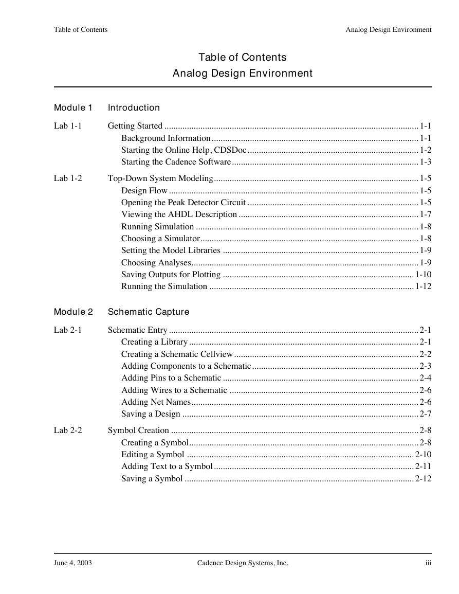
Introduction
Lab 1-1 Getting Started
Background Information
Starting the Online Help, CDSDoc
Starting the Cadence Software
Lab 1-2 Top-Down System Modeling
Design Flow
Opening the Peak Detector Circuit
Viewing the AHDL Description
Running Simulation
Choosing a Simulator
Setting the Model Libraries
Choosing Analyses
Saving Outputs for Plotting
Running the Simulation
Schematic Capture
Lab 2-1 Schematic Entry
Creating a Library
Creating a Schematic Cellview
Adding Components to a Schematic
Adding Pins to a Schematic
Adding Wires to a Schematic
Adding Net Names
Saving a Design
Lab 2-2 Symbol Creation
Creating a Symbol
Editing a Symbol
Adding Text to a Symbol
Saving a Symbol
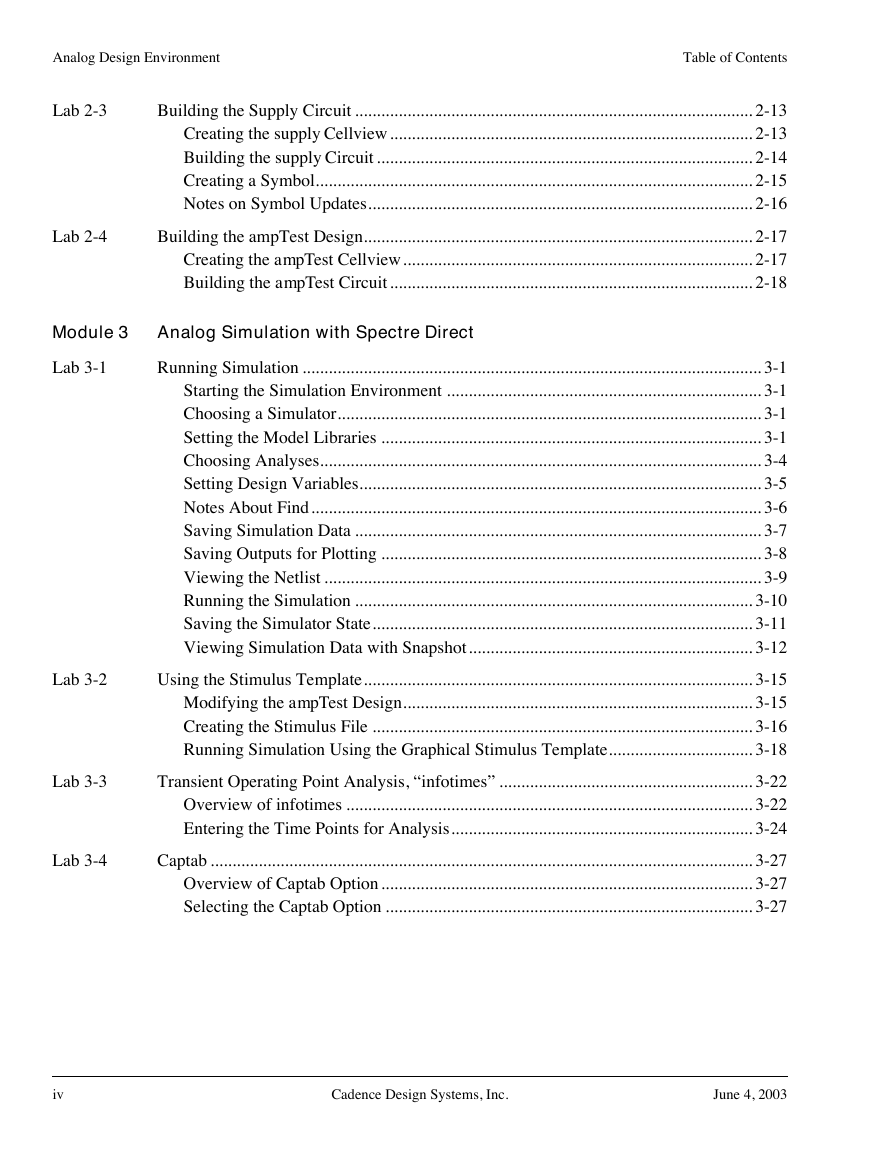
Lab 2-3 Building the Supply Circuit
Creating the supply Cellview
Building the supply Circuit
Creating a Symbol
Notes on Symbol Updates
Lab 2-4 Building the ampTest Design
Creating the ampTest Cellview
Building the ampTest Circuit
Analog Simulation with Spectre Direct
Lab 3-1 Running Simulation
Starting the Simulation Environment
Choosing a Simulator
Setting the Model Libraries
Choosing Analyses
Setting Design Variables
Notes About Find
Saving Simulation Data
Saving Outputs for Plotting
Viewing the Netlist
Running the Simulation
Saving the Simulator State
Viewing Simulation Data with Snapshot
Lab 3-2 Using the Stimulus Template
Modifying the ampTest Design
Creating the Stimulus File
Running Simulation Using the Graphical Stimulus Template
Lab 3-3 Transient Operating Point Analysis, “infotimes”
Overview of infotimes
Entering the Time Points for Analysis
Lab 3-4 Captab
Overview of Captab Option
Selecting the Captab Option
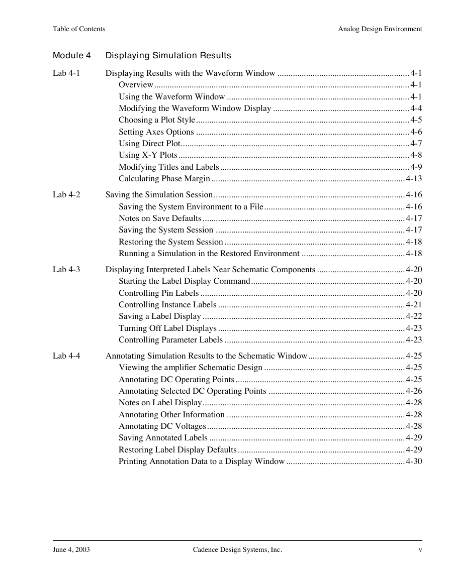
Displaying Simulation Results
Lab 4-1 Displaying Results with the Waveform Window
Overview
Using the Waveform Window
Modifying the Waveform Window Display
Choosing a Plot Style
Setting Axes Options
Using Direct Plot
Using X-Y Plots
Modifying Titles and Labels
Calculating Phase Margin
Lab 4-2 Saving the Simulation Session
Saving the System Environment to a File
Notes on Save Defaults
Saving the System Session
Restoring the System Session
Running a Simulation in the Restored Environment
Lab 4-3 Displaying Interpreted Labels Near Schematic Components
Starting the Label Display Command
Controlling Pin Labels
Controlling Instance Labels
Saving a Label Display
Turning Off Label Displays
Controlling Parameter Labels
Lab 4-4 Annotating Simulation Results to the Schematic Window
Viewing the amplifier Schematic Design
Annotating DC Operating Points
Annotating Selected DC Operating Points
Notes on Label Display
Annotating Other Information
Annotating DC Voltages
Saving Annotated Labels
Restoring Label Display Defaults
Printing Annotation Data to a Display Window
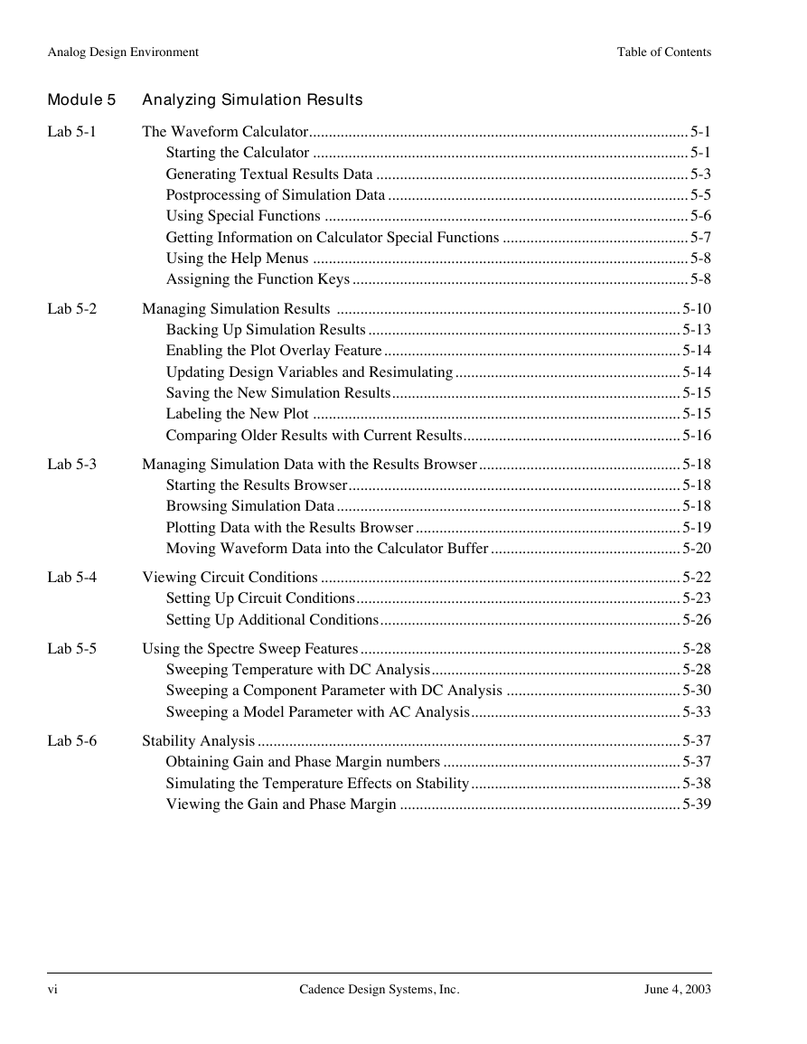
Analyzing Simulation Results
Lab 5-1 The Waveform Calculator
Starting the Calculator
Generating Textual Results Data
Postprocessing of Simulation Data
Using Special Functions
Getting Information on Calculator Special Functions
Using the Help Menus
Assigning the Function Keys
Lab 5-2 Managing Simulation Results
Backing Up Simulation Results
Enabling the Plot Overlay Feature
Updating Design Variables and Resimulating
Saving the New Simulation Results
Labeling the New Plot
Comparing Older Results with Current Results
Lab 5-3 Managing Simulation Data with the Results Browser
Starting the Results Browser
Browsing Simulation Data
Plotting Data with the Results Browser
Moving Waveform Data into the Calculator Buffer
Lab 5-4 Viewing Circuit Conditions
Setting Up Circuit Conditions
Setting Up Additional Conditions
Lab 5-5 Using the Spectre Sweep Features
Sweeping Temperature with DC Analysis
Sweeping a Component Parameter with DC Analysis
Sweeping a Model Parameter with AC Analysis
Lab 5-6 Stability Analysis
Obtaining Gain and Phase Margin numbers
Simulating the Temperature Effects on Stability
Viewing the Gain and Phase Margin
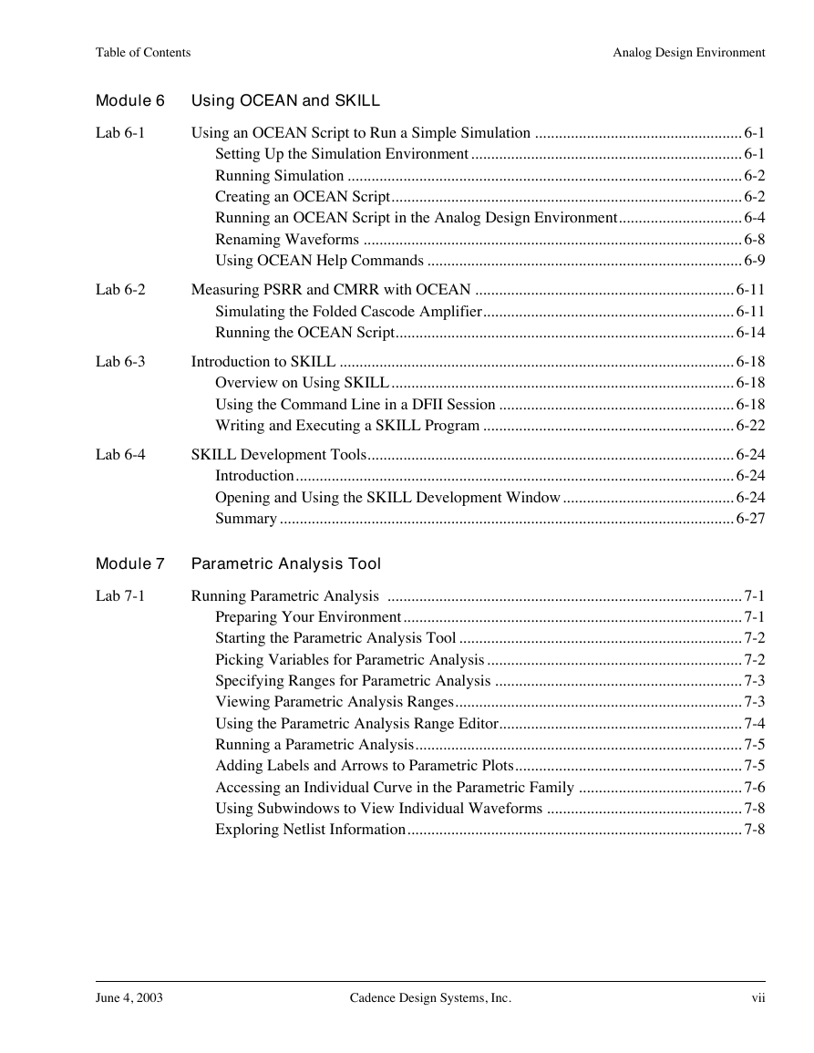
Using OCEAN and SKILL
Lab 6-1 Using an OCEAN Script to Run a Simple Simulation
Setting Up the Simulation Environment
Running Simulation
Creating an OCEAN Script
Running an OCEAN Script in the Analog Design Environment
Renaming Waveforms
Using OCEAN Help Commands
Lab 6-2 Measuring PSRR and CMRR with OCEAN
Simulating the Folded Cascode Amplifier
Running the OCEAN Script
Lab 6-3 Introduction to SKILL
Overview on Using SKILL
Using the Command Line in a DFII Session
Writing and Executing a SKILL Program
Lab 6-4 SKILL Development Tools
Introduction
Opening and Using the SKILL Development Window
Summary
Parametric Analysis Tool
Lab 7-1 Running Parametric Analysis
Preparing Your Environment
Starting the Parametric Analysis Tool
Picking Variables for Parametric Analysis
Specifying Ranges for Parametric Analysis
Viewing Parametric Analysis Ranges
Using the Parametric Analysis Range Editor
Running a Parametric Analysis
Adding Labels and Arrows to Parametric Plots
Accessing an Individual Curve in the Parametric Family
Using Subwindows to View Individual Waveforms
Exploring Netlist Information
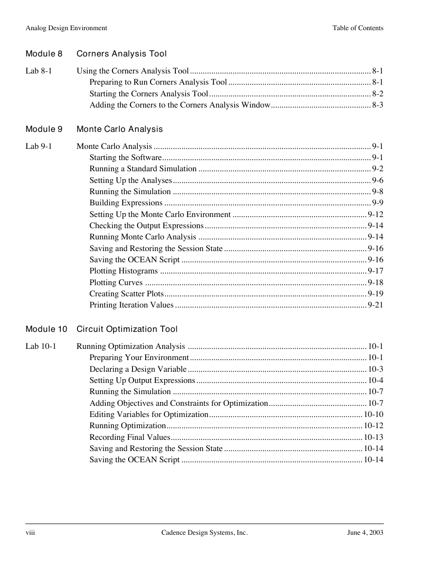
Corners Analysis Tool
Lab 8-1 Using the Corners Analysis Tool
Preparing to Run Corners Analysis Tool
Starting the Corners Analysis Tool
Adding the Corners to the Corners Analysis Window
Monte Carlo Analysis
Lab 9-1 Monte Carlo Analysis
Starting the Software
Running a Standard Simulation
Setting Up the Analyses
Running the Simulation
Building Expressions
Setting Up the Monte Carlo Environment
Checking the Output Expressions
Running Monte Carlo Analysis
Saving and Restoring the Session State
Saving the OCEAN Script
Plotting Histograms
Plotting Curves
Creating Scatter Plots
Printing Iteration Values
Circuit Optimization Tool
Lab 10-1 Running Optimization Analysis
Preparing Your Environment
Declaring a Design Variable
Setting Up Output Expressions
Running the Simulation
Adding Objectives and Constraints for Optimization
Editing Variables for Optimization
Running Optimization
Recording Final Values
Saving and Restoring the Session State
Saving the OCEAN Script
Exploring CDF
Lab 11-1 The CDF User Interface
Copying the Design to Another Name
Adding the InlineAmp to the InlineAmpTest Design
Copying the nmos4 Cell and CDF
Starting the CDF User Interface
Editing the Base Cell CDF
Viewing Component Parameter Prompts
Viewing the Inline Subcircuit Models
Setting Default Values for Component Parameters
Adding Component Parameters in the CDF
Editing Simulation Information
Lab 11-2 CDF Effects in Simulation
Opening the InlineAmpTest Design
Modifying the Design
Verifying the Netlist
Running Simulation
Comparing Inline Subcircuits with Subcircuits
Running Simulation and Viewing Differences
Inline Subcircuits
Lab 12-1 Creating a Parasitic Transistor Model
Copying the npn Component
Editing the CDF of the npnpar Component
Updating the InlineAmp Schematic
Adding an Instance Parameter
Running Simulation and Viewing Results
Saving All Voltages and Terminal Currents
Lab 12-2 Using Subcircuit Cells
Adding the OpAmp Macromodel
Viewing the Opamp Macromodel
Running Simulation and Viewing Results
Using Subcircuits with No Schematics
Viewing the CDF of the vcvsOpampMacro Component
Running Simulation and Viewing Results
Lab 12-3 Adding a Subcircuit Representation
Creating a Primitive Cellview
Editing the CDF of a Macromodel Cell
Adding the model Component Parameter
Adding Cell CDF Parameters for the Dynamic Macromodel File
Editing the CDF Simulation Information for the Macromodel Cell
Placing the InlineAmp Component Back in the Design
Inherited Connections
Lab 13-1 Inherited Connections
Studying a Design with Inherited Connections
Running Simulation
Lab 13-2 Using Inherited Connections with the ampTest Design
Copying the Design to Another Name
Adding the inhamp Circuit to the inhampTest Design
Modifying the inhamp Design
Modifying the inhampTest Circuit
Adding netSet Properties
Viewing Overridden Properties
Running Simulation
Modify netSet Properties and Simulate Again
Hierarchy Editor
Lab 14-1 Creating a Configuration File with the Hierarchy Editor
Creating a Configuration
Lab 14-2 Running a Simulation with Subcircuits
Modifying the Design
Starting the Simulation Environment
Running the Simulation
Lab 14-3 Rerunning Simulation with the Schematic View
Viewing the Design Hierarchy and Updating the Configuration
Running Simulation and Comparing Results
Parasitic Simulation Setup
Lab 15-1 Simulating a Schematic Without Parasitics
Overview
Scenario
Starting the Software
Opening the Test Fixture and Simulation Environment
Running Simulation and Measuring Propagation Delay
Parasitic Simulation Setup and Analysis
Lab 16-1 Parasitic Simulation Flow
Starting the Flow
Opening the Test Fixture Schematic
Creating the Configuration View
Reviewing the Design Schematic and Layout
Extracting Designed Devices and Running Assura LVS
Setting Up LVS
Running LVS Before RCX
Running RCX - All Nets in the Design
Building the av_analog_extracted View
Running Simulation without Parasitics
Measuring Propagation Delay with the Calculator
Choosing a Configuration
Running Simulation with Parasitics
Plotting Simulation Data from the Results Browser
Measuring Parasitic Propagation Delay with the Calculator
Backannotating Parasitic Values
Parasitic Probing
Whole Net Probing
Point to Point Probing
Net to Net Probing
Summary
Diva Parasitic Extraction and Simulation
Lab A-1 Simulating a Schematic with Parasitics Using the Diva Layout Flow
Scenario
Opening the Design Schematic
Opening the Design Layout
Extracting the Layout and Running LVS Without Parasitics
Extracting the Layout and Running LVS with Parasitics
Exploring the Parasitic Resistor Model
Verifying LVS Results
Backannotating
Parasitic Probing
Building the analog_extracted View for the Design
Opening the Test Fixture Schematic
Creating a Configuration
Editing the Configuration to Run a Full Parasitic Simulation
Running Parasitic Simulation
Waveform Analysis in the Extracted View
Running Selective Parasitic Simulation
Running Selective Parasitic Simulation Again
Running Selective Parasitic Simulation on One Net
Schematic Waveform Analysis
Closing All Windows
Using the WaveScan Tool
Lab B-1 Using the WaveScan Tool
Starting WaveScan
Using the WaveScan Calculator
Using the WaveScan Zoom, Markers, and Labels
Waveforms in the Graph Display Environment
Spectre MDL
Lab C-1 Using Spectre MDL
Intro to Spectre MDL
Passing Parameters into Control Files
Autostop
Corners
Search
Foreach
HSPICE Compatibility
Using “dcmatch” Analysis
Lab D-1 dcmatch
Opening the Amplifier Schematic and Starting the Simulation Environment
Running dcmatch Analysis and Viewing Results
Advanced Topics
Lab E-1 Verilog-A Overview
Using the Verilog-A Modelwriter Tool to Simulate a VCO
Test Your VCO Design
Preparing for the Next Lab



 2023年江西萍乡中考道德与法治真题及答案.doc
 2012年重庆南川中考生物真题及答案.doc
 2013年江西师范大学地理学综合及文艺理论基础考研真题.doc
 2020年四川甘孜小升初语文真题及答案I卷.doc
 2020年注册岩土工程师专业基础考试真题及答案.doc
 2023-2024学年福建省厦门市九年级上学期数学月考试题及答案.doc
 2021-2022学年辽宁省沈阳市大东区九年级上学期语文期末试题及答案.doc
 2022-2023学年北京东城区初三第一学期物理期末试卷及答案.doc
 2018上半年江西教师资格初中地理学科知识与教学能力真题及答案.doc
 2012年河北国家公务员申论考试真题及答案-省级.doc
 2020-2021学年江苏省扬州市江都区邵樊片九年级上学期数学第一次质量检测试题及答案.doc
 2022下半年黑龙江教师资格证中学综合素质真题及答案.doc