logo资料库

pg153-axi-quad-spi.pdf

第1页 / 共114页
第2页 / 共114页
第3页 / 共114页
第4页 / 共114页
第5页 / 共114页
第6页 / 共114页
第7页 / 共114页
第8页 / 共114页
资料共114页,剩余部分请下载后查看
AXI Quad SPI v3.2
Table of Contents
IP Facts
Ch. 1: Overview
Legacy Mode
Standard SPI Mode
Dual/Quad SPI Mode
Common Information for Both SPI Modes
AXI4 Interface
Enhanced Mode
XIP Mode
Dual Quad SPI Mode
Core Internal Submodules
Enable Performance Mode Not Selected
AXI4-Lite Interface Module
SPI Register Module
Interrupt Controller Register Set Module
SPI Module
Optional FIFOs
STARTUPEn Module
Enable STARTUPE2 Primitive Parameter
Enable STARTUPE3 Primitive Parameter
Quad SPI Control Logic Module
Feature Summary
Unsupported Features
Licensing and Ordering Information
Ch. 2: Product Specification
Standards
Performance
Resource Utilization
Port Descriptions
Register Space (Legacy and Enhanced Non-XIP Mode)
Register Details
Software Reset Register
SPI Control Register
SPI Status Register
SPI Data Transmit Register
Dual/Quad Mode
SPI Data Receive Register
SPI Slave Select Register
SPI Transmit FIFO Occupancy Register
SPI Receive FIFO Occupancy Register
Interrupt Register Set Description
Device Global Interrupt Enable Register
IP Interrupt Status Register (IPISR)
IP Interrupt Enable Register (IPIER)
XIP Mode
XIP Mode Commands
XIP Configuration Register
XIP Status Register
Specification Exceptions
Exceptions from the Motorola M68HC11-Rev. 4.0 Reference Manual
Other Exceptions
Ch. 3: Designing with the Core
General Design Guidelines
Functionality Based on AXI Interfaces
AXI4-Lite Interface
AXI4 Interface (Enhanced Mode)
AXI4 Read-Only Interface (XIP Mode)
Standard SPI Device Features with Only AXI4-Lite Interface
AXI4-Lite Interface Functionality in Standard SPI Multi-Master Configuration
AXI4-Lite Interface Standard SPI Mode — Optional FIFOs in Legacy Mode
AXI4-Lite Interface Dual/Quad SPI Mode — Optional FIFO Depth
AXI4-Lite Interface SPI Master Loopback Operation
AXI4-Lite Interface Hardware Error Detection
Setting the Frequency Ratio Parameter
AXI4-Lite Interface SPI Slave Mode — Standard SPI Configuration in Legacy Mode Only
Using the Enable STARTUPEn Primitive Parameter
Enable STARTUPEn Primitive is Selected
Core Behavior and Ports
Using the Dual Quad Mode
Enable STARTUPEn Primitive is Not Selected
Core Behavior and Ports
Core Behavior in Legacy and Enhanced Non-XIP Mode
Core Behavior in XIP Mode
Winbond Memory
Micron Memory
Spansion Memory
Commonly Supported Commands for Dual SPI and Mixed Memory Mode
Commonly Supported Commands for Quad SPI and Mixed Memory Mode
XIP Mode Commands
Winbond Memory (Ex: W25Q64VSFIG)
Micron Memory (Ex: N25Q256)
Spansion Memory (Ex: S70FL01GS)
Clocking (SPI Clock Phase and Polarity Control)
Resets
Protocol Description
AXI Quad SPI Core Behavior in Legacy and Enhanced Mode
Mode = Dual
Slave Device = Mixed
Slave Device = Winbond
Slave Device = Micron
Slave Device = Spansion
Mode = Quad
Slave Device = Mixed
Slave Device = Winbond
Slave Device = Micron
Slave Device = Spansion
Core Behavior in XIP Mode
Standard SPI Mode Transactions
SPI Master Device with/without FIFOs and Slave Select Vector Asserted Manually Using SPICR Bit 7
SPI Master and Slave Devices without FIFOs Performing One 8-bit/16-bit/ 32-bit Transfer (Optional Mode)
SPI Master and Slave Devices where Registers/FIFOs are Filled Before the SPI Transfer Begins and Multiple Discrete 8-bit Transfers are Performed (Optional Mode)
SPI Master and Slave Devices with FIFOs Where Some Initial Data is Written to FIFOs, the SPI Transfer is Started, Data is Written to the FIFOs as Fast or Faster than the SPI Transfer and Multiple Discrete 8-bit Transfers are Performed (Optional Mode).
Dual/Quad SPI Mode Transactions
Dual/Quad Mode SPI Configuration
Transfer Formats
CPHA Equals Zero Transfer Format
CPHA Equals One Transfer Format
SPI Protocol Slave Select Assertion Modes
SPI Protocol with Automatic Slave Select Assertion
SPI Protocol with Manual Slave Select Assertion
Beginning and Ending SPI Transfers
Transfer Begin Period
Transfer End Period
Ch. 4: Design Flow Steps
Customizing and Generating the Core
AXI Interface Options
SPI Options
Remaining Options
User Parameters
Output Generation
Constraining the Core
Required Constraints
Write Operation to SPI
Read Operation
Constraining the IP
Constraints in Dual Quad Mode
Device, Package, and Speed Grade Selections
Clock Frequencies
Clock Management
Clock Placement
Banking
Transceiver Placement
I/O Standard and Placement
Simulation
Synthesis and Implementation
Ch. 5: Example Design
Overview
Implementing the Example Design
Testing the Example Design on a KC705 Board
Legacy Mode and Performance Mode Example Design Behavior
XIP Mode Example Design Behavior
Simulating the Example Design
Setting up the Simulation
Example Programming Sequence
Write Enable Command Sequence
Erase Command Sequence
Write Data Command Sequence
Read Data Command Sequence
Ch. 6: Test Bench
Overview
Checking Results
Appx. A: Verification, Compliance, and Interoperability
Appx. B: Migrating and Upgrading
Migrating to the Vivado Design Suite
Upgrading in the Vivado Design Suite
Appx. C: Debugging
Finding Help on Xilinx.com
Documentation
Answer Records
Technical Support
Vivado Design Suite Debug Feature
Hardware Debug
Interface Debug
AXI4-Lite Interfaces
AXI4 Interfaces
Enhanced Mode Debug
XIP Mode Debug
Appx. D: Additional Resources and Legal Notices
Xilinx Resources
References
Revision History
Please Read: Important Legal Notices
AXI Quad SPI v3.2 LogiCORE IP Product Guide Vivado Design Suite PG153 April 4, 2018
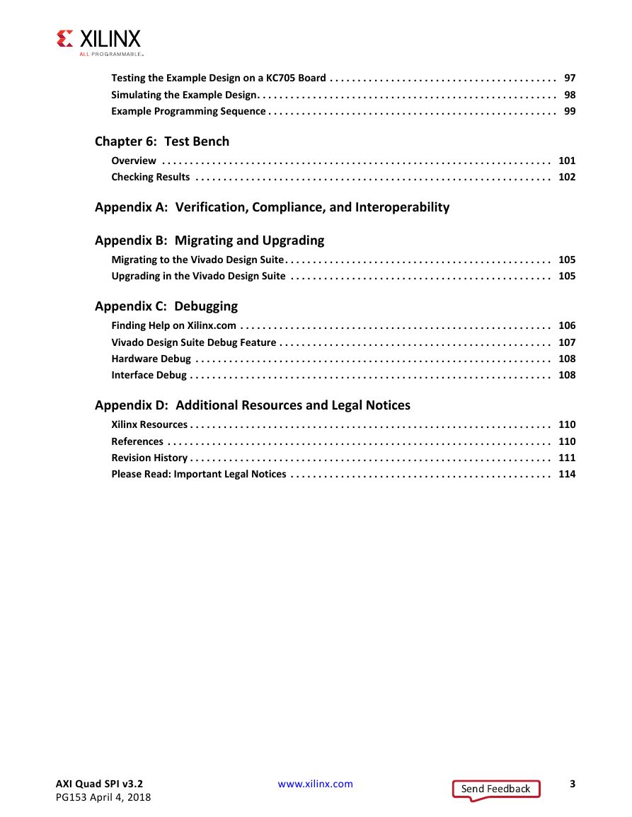
Table of Contents IP Facts Chapter 1: Overview Legacy Mode . . . . . . . . . . . . . . . . . . . . . . . . . . . . . . . . . . . . . . . . . . . . . . . . . . . . . . . . . . . . . . . . . . . . . 6 AXI4 Interface. . . . . . . . . . . . . . . . . . . . . . . . . . . . . . . . . . . . . . . . . . . . . . . . . . . . . . . . . . . . . . . . . . . . . 9 Core Internal Submodules. . . . . . . . . . . . . . . . . . . . . . . . . . . . . . . . . . . . . . . . . . . . . . . . . . . . . . . . . . 11 Feature Summary. . . . . . . . . . . . . . . . . . . . . . . . . . . . . . . . . . . . . . . . . . . . . . . . . . . . . . . . . . . . . . . . . 13 Unsupported Features. . . . . . . . . . . . . . . . . . . . . . . . . . . . . . . . . . . . . . . . . . . . . . . . . . . . . . . . . . . . . 16 Licensing and Ordering Information. . . . . . . . . . . . . . . . . . . . . . . . . . . . . . . . . . . . . . . . . . . . . . . . . . 16 Chapter 2: Product Specification Standards . . . . . . . . . . . . . . . . . . . . . . . . . . . . . . . . . . . . . . . . . . . . . . . . . . . . . . . . . . . . . . . . . . . . . . . 17 Performance. . . . . . . . . . . . . . . . . . . . . . . . . . . . . . . . . . . . . . . . . . . . . . . . . . . . . . . . . . . . . . . . . . . . . 17 Resource Utilization. . . . . . . . . . . . . . . . . . . . . . . . . . . . . . . . . . . . . . . . . . . . . . . . . . . . . . . . . . . . . . . 18 Port Descriptions . . . . . . . . . . . . . . . . . . . . . . . . . . . . . . . . . . . . . . . . . . . . . . . . . . . . . . . . . . . . . . . . . 19 Register Space (Legacy and Enhanced Non-XIP Mode) . . . . . . . . . . . . . . . . . . . . . . . . . . . . . . . . . . . 23 Specification Exceptions . . . . . . . . . . . . . . . . . . . . . . . . . . . . . . . . . . . . . . . . . . . . . . . . . . . . . . . . . . . 44 Chapter 3: Designing with the Core General Design Guidelines . . . . . . . . . . . . . . . . . . . . . . . . . . . . . . . . . . . . . . . . . . . . . . . . . . . . . . . . . 47 Clocking (SPI Clock Phase and Polarity Control) . . . . . . . . . . . . . . . . . . . . . . . . . . . . . . . . . . . . . . . . 63 Resets . . . . . . . . . . . . . . . . . . . . . . . . . . . . . . . . . . . . . . . . . . . . . . . . . . . . . . . . . . . . . . . . . . . . . . . . . . 63 Protocol Description . . . . . . . . . . . . . . . . . . . . . . . . . . . . . . . . . . . . . . . . . . . . . . . . . . . . . . . . . . . . . . 64 Chapter 4: Design Flow Steps Customizing and Generating the Core . . . . . . . . . . . . . . . . . . . . . . . . . . . . . . . . . . . . . . . . . . . . . . . . 81 Constraining the Core . . . . . . . . . . . . . . . . . . . . . . . . . . . . . . . . . . . . . . . . . . . . . . . . . . . . . . . . . . . . . 85 Simulation . . . . . . . . . . . . . . . . . . . . . . . . . . . . . . . . . . . . . . . . . . . . . . . . . . . . . . . . . . . . . . . . . . . . . . 93 Synthesis and Implementation . . . . . . . . . . . . . . . . . . . . . . . . . . . . . . . . . . . . . . . . . . . . . . . . . . . . . . 93 Chapter 5: Example Design Overview . . . . . . . . . . . . . . . . . . . . . . . . . . . . . . . . . . . . . . . . . . . . . . . . . . . . . . . . . . . . . . . . . . . . . . . 94 Implementing the Example Design. . . . . . . . . . . . . . . . . . . . . . . . . . . . . . . . . . . . . . . . . . . . . . . . . . . 95 AXI Quad SPI v3.2 PG153 April 4, 2018 www.xilinx.com 2 Send Feedback
Testing the Example Design on a KC705 Board . . . . . . . . . . . . . . . . . . . . . . . . . . . . . . . . . . . . . . . . . 97 Simulating the Example Design. . . . . . . . . . . . . . . . . . . . . . . . . . . . . . . . . . . . . . . . . . . . . . . . . . . . . . 98 Example Programming Sequence . . . . . . . . . . . . . . . . . . . . . . . . . . . . . . . . . . . . . . . . . . . . . . . . . . . . 99 Chapter 6: Test Bench Overview . . . . . . . . . . . . . . . . . . . . . . . . . . . . . . . . . . . . . . . . . . . . . . . . . . . . . . . . . . . . . . . . . . . . . . 101 Checking Results . . . . . . . . . . . . . . . . . . . . . . . . . . . . . . . . . . . . . . . . . . . . . . . . . . . . . . . . . . . . . . . . 102 Appendix A: Verification, Compliance, and Interoperability Appendix B: Migrating and Upgrading Migrating to the Vivado Design Suite. . . . . . . . . . . . . . . . . . . . . . . . . . . . . . . . . . . . . . . . . . . . . . . . 105 Upgrading in the Vivado Design Suite . . . . . . . . . . . . . . . . . . . . . . . . . . . . . . . . . . . . . . . . . . . . . . . 105 Appendix C: Debugging Finding Help on Xilinx.com . . . . . . . . . . . . . . . . . . . . . . . . . . . . . . . . . . . . . . . . . . . . . . . . . . . . . . . . 106 Vivado Design Suite Debug Feature . . . . . . . . . . . . . . . . . . . . . . . . . . . . . . . . . . . . . . . . . . . . . . . . . 107 Hardware Debug . . . . . . . . . . . . . . . . . . . . . . . . . . . . . . . . . . . . . . . . . . . . . . . . . . . . . . . . . . . . . . . . 108 Interface Debug . . . . . . . . . . . . . . . . . . . . . . . . . . . . . . . . . . . . . . . . . . . . . . . . . . . . . . . . . . . . . . . . . 108 Appendix D: Additional Resources and Legal Notices Xilinx Resources . . . . . . . . . . . . . . . . . . . . . . . . . . . . . . . . . . . . . . . . . . . . . . . . . . . . . . . . . . . . . . . . . 110 References . . . . . . . . . . . . . . . . . . . . . . . . . . . . . . . . . . . . . . . . . . . . . . . . . . . . . . . . . . . . . . . . . . . . . 110 Revision History . . . . . . . . . . . . . . . . . . . . . . . . . . . . . . . . . . . . . . . . . . . . . . . . . . . . . . . . . . . . . . . . . 111 Please Read: Important Legal Notices . . . . . . . . . . . . . . . . . . . . . . . . . . . . . . . . . . . . . . . . . . . . . . . 114 AXI Quad SPI v3.2 PG153 April 4, 2018 www.xilinx.com 3 Send Feedback
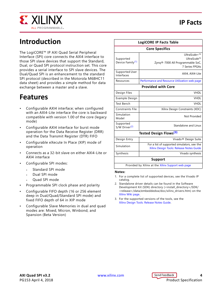
Introduction The LogiCORE™ IP AXI Quad Serial Peripheral Interface (SPI) core connects the AXI4 interface to those SPI slave devices that support the Standard, Dual, or Quad SPI protocol instruction set. This core provides a serial interface to SPI slave devices. The Dual/Quad SPI is an enhancement to the standard SPI protocol (described in the Motorola M68HC11 data sheet) and provides a simple method for data exchange between a master and a slave. Features • Configurable AXI4 interface; when configured with an AXI4-Lite interface the core is backward compatible with version 1.00 of the core (legacy mode) Configurable AXI4 interface for burst mode operation for the Data Receive Register (DRR) and the Data Transmit Register (DTR) FIFO Configurable eXecute In Place (XIP) mode of operation Connects as a 32-bit slave on either AXI4-Lite or AXI4 interface Configurable SPI modes: Standard SPI mode ° Dual SPI mode ° ° Quad SPI mode Programmable SPI clock phase and polarity Configurable FIFO depth (16 or 256 element deep in Dual/Quad/Standard SPI mode) and fixed FIFO depth of 64 in XIP mode Configurable Slave Memories in dual and quad modes are: Mixed, Micron, Winbond, and Spansion (Beta Version) • • • • • • • IP Facts LogiCORE IP Facts Table Core Specifics UltraScale+™ UltraScale™ Zynq®-7000 All Programmable SoC, 7 Series FPGAs AXI4, AXI4-Lite Performance and Resource Utilization web page Provided with Core VHDL VHDL VHDL Xilinx Design Constraints (XDC) Not Provided Standalone and Linux Tested Design Flows(3) Vivado® Design Suite For a list of supported simulators, see the Xilinx Design Tools: Release Notes Guide Vivado synthesis Support Supported Device Family(1) Supported User Interfaces Resources Design Files Example Design Test Bench Constraints File Simulation Model Supported S/W Driver(2) Design Entry Simulation Synthesis Provided by Xilinx at the Xilinx Support web page Notes: 1. For a complete list of supported devices, see the Vivado IP catalog. 2. Standalone driver details can be found in the Software Development Kit (SDK) directory (/SDK/ /data/embeddedsw/doc/xilinx_drivers.htm) on the Xilinx Wiki page. 3. For the supported versions of the tools, see the Xilinx Design Tools: Release Notes Guide. AXI Quad SPI v3.2 PG153 April 4, 2018 www.xilinx.com 4 Product Specification Send Feedback
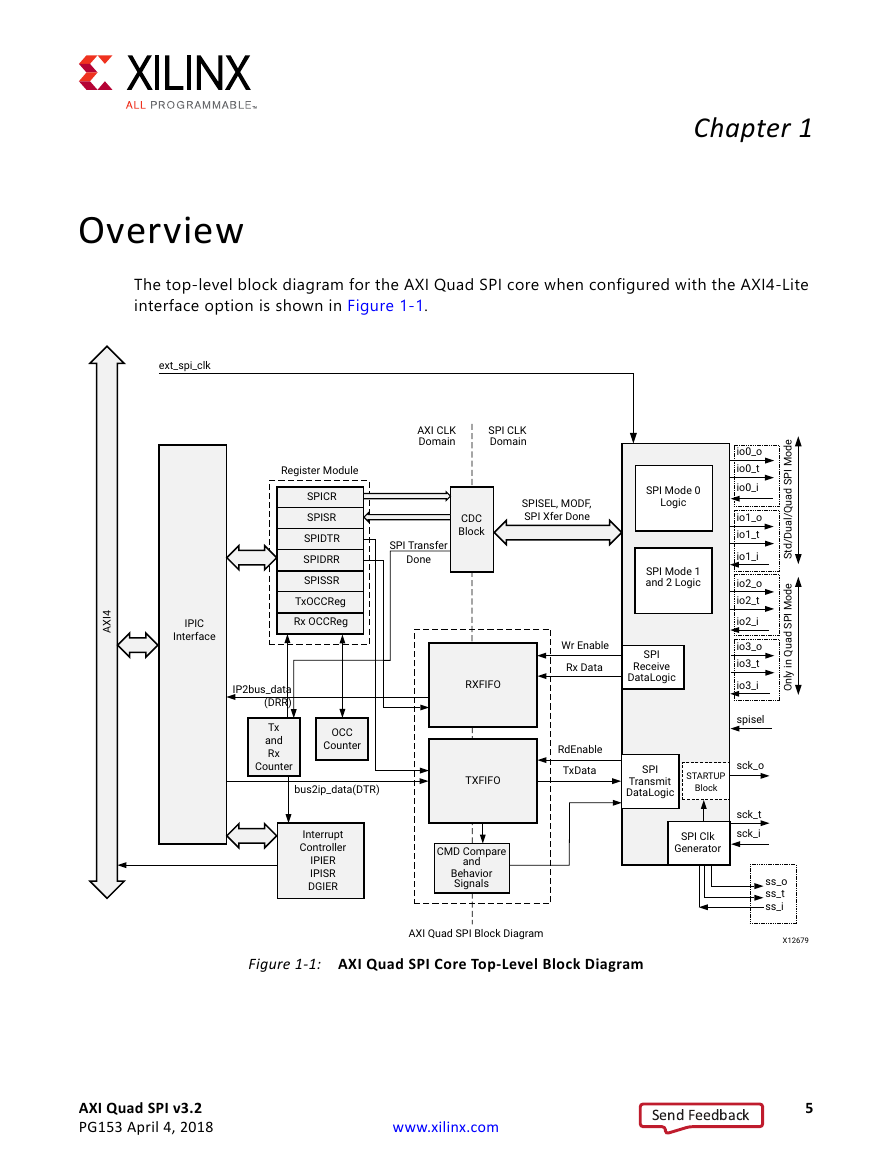
Chapter 1 Overview The top-level block diagram for the AXI Quad SPI core when configured with the AXI4-Lite interface option is shown in Figure 1-1. X-Ref Target - Figure 1-1 Figure 1-1: AXI Quad SPI Core Top-Level Block Diagram AXI Quad SPI v3.2 PG153 April 4, 2018 www.xilinx.com 5 Send Feedback
The choice of either AXI4-Lite or AXI4 interface is based on the Enable Performance Mode option in the Vivado® Integrated Design Environment (IDE) (see Chapter 4). Performance mode is disabled by default which selects the AXI4-Lite interface. The core always operates as a slave IP when the AXI4 interface is selected. Chapter 1: Overview Legacy Mode Legacy mode is selected when the Enable Performance Mode option in the Vivado Integrated Design Environment (IDE) is disabled. Legacy mode uses the AXI4-Lite interface and is fully backward compatible with all the older versions of the AXI Quad SPI core in terms of functionality, register bit placement, and register access. The AXI Quad SPI core, when configured in standard SPI mode, is a full-duplex synchronous channel that supports a four-wire interface (receive, transmit, clock, and slave-select) between a master and a selected slave. When configured in Dual/Quad SPI mode, this core supports additional pins for interfacing with external memory. These additional pins are used while transmitting the command, address, and data based on the control register settings and command used. The core supports the manual slave select mode as the default mode of operation for slave select mode. This mode allows manual control of the slave select line with the data written to the slave select register, thereby allowing transfers of an arbitrary number of elements without toggling the slave select line between elements. However, before starting a new transfer, the slave select line must be toggled. The other mode related to slave select is automatic slave select mode. In this mode, the slave select line is toggled automatically after each element transfer (when FIFO is disabled). This mode, which is supported only in standard SPI mode, is described in more detail in SPI Protocol Slave Select Assertion Modes in Chapter 3. The core functionality is divided into standard SPI mode and dual and quad SPI mode. The functionality for each mode differs in the way the slave memory works. Standard SPI Mode Standard SPI mode is selected when the Mode option in the Vivado IDE is set to Standard. The relevant parameters in this mode are: • Mode • • • No. of Slaves • Enable STARTUPE2 Primitive Transaction Width Frequency Ratio AXI Quad SPI v3.2 PG153 April 4, 2018 www.xilinx.com 6 Send Feedback
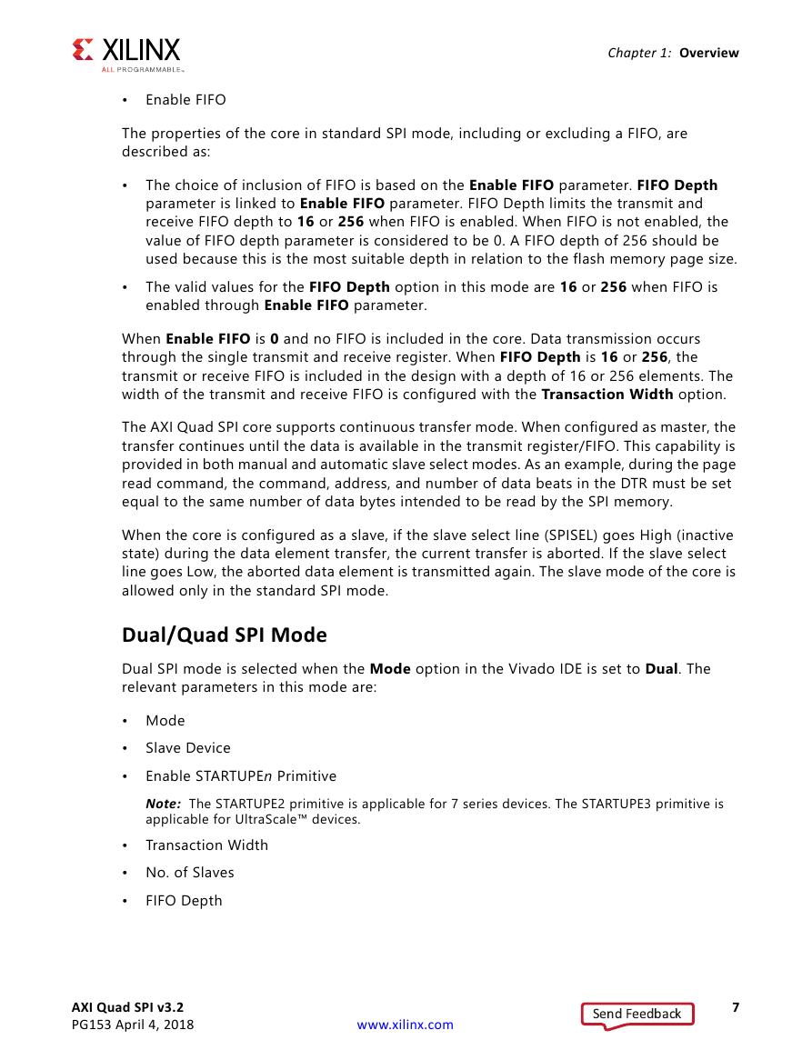
Chapter 1: Overview Enable FIFO • The properties of the core in standard SPI mode, including or excluding a FIFO, are described as: • The choice of inclusion of FIFO is based on the Enable FIFO parameter. FIFO Depth parameter is linked to Enable FIFO parameter. FIFO Depth limits the transmit and receive FIFO depth to 16 or 256 when FIFO is enabled. When FIFO is not enabled, the value of FIFO depth parameter is considered to be 0. A FIFO depth of 256 should be used because this is the most suitable depth in relation to the flash memory page size. The valid values for the FIFO Depth option in this mode are 16 or 256 when FIFO is enabled through Enable FIFO parameter. • When Enable FIFO is 0 and no FIFO is included in the core. Data transmission occurs through the single transmit and receive register. When FIFO Depth is 16 or 256, the transmit or receive FIFO is included in the design with a depth of 16 or 256 elements. The width of the transmit and receive FIFO is configured with the Transaction Width option. The AXI Quad SPI core supports continuous transfer mode. When configured as master, the transfer continues until the data is available in the transmit register/FIFO. This capability is provided in both manual and automatic slave select modes. As an example, during the page read command, the command, address, and number of data beats in the DTR must be set equal to the same number of data bytes intended to be read by the SPI memory. When the core is configured as a slave, if the slave select line (SPISEL) goes High (inactive state) during the data element transfer, the current transfer is aborted. If the slave select line goes Low, the aborted data element is transmitted again. The slave mode of the core is allowed only in the standard SPI mode. Dual/Quad SPI Mode Dual SPI mode is selected when the Mode option in the Vivado IDE is set to Dual. The relevant parameters in this mode are: • Mode • • Slave Device Enable STARTUPEn Primitive Note: The STARTUPE2 primitive is applicable for 7 series devices. The STARTUPE3 primitive is applicable for UltraScale™ devices. Transaction Width • • No. of Slaves • FIFO Depth AXI Quad SPI v3.2 PG153 April 4, 2018 www.xilinx.com 7 Send Feedback
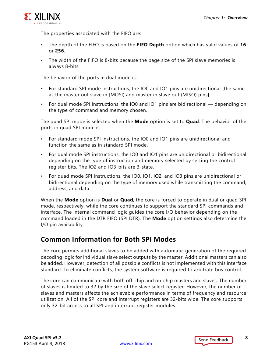
Chapter 1: Overview The properties associated with the FIFO are: • The depth of the FIFO is based on the FIFO Depth option which has valid values of 16 or 256. The width of the FIFO is 8-bits because the page size of the SPI slave memories is always 8-bits. • • The behavior of the ports in dual mode is: • For standard SPI mode instructions, the IO0 and IO1 pins are unidirectional [the same as the master out slave in (MOSI) and master in slave out (MISO) pins]. For dual mode SPI instructions, the IO0 and IO1 pins are bidirectional — depending on the type of command and memory chosen. The quad SPI mode is selected when the Mode option is set to Quad. The behavior of the ports in quad SPI mode is: • For standard mode SPI instructions, the IO0 and IO1 pins are unidirectional and function the same as in standard SPI mode. For dual mode SPI instructions, the IO0 and IO1 pins are unidirectional or bidirectional depending on the type of instruction and memory selected by setting the control register bits. The IO2 and IO3-bits are 3-state. For quad mode SPI instructions, the IO0, IO1, IO2, and IO3 pins are unidirectional or bidirectional depending on the type of memory used while transmitting the command, address, and data. • • When the Mode option is Dual or Quad, the core is forced to operate in dual or quad SPI mode, respectively, while the core continues to support the standard SPI commands and interface. The internal command logic guides the core I/O behavior depending on the command loaded in the DTR FIFO (SPI DTR). The Mode option settings also determine the I/O pin availability. Common Information for Both SPI Modes The core permits additional slaves to be added with automatic generation of the required decoding logic for individual slave select outputs by the master. Additional masters can also be added. However, detection of all possible conflicts is not implemented with this interface standard. To eliminate conflicts, the system software is required to arbitrate bus control. The core can communicate with both off-chip and on-chip masters and slaves. The number of slaves is limited to 32 by the size of the slave select register. However, the number of slaves and masters affects the achievable performance in terms of frequency and resource utilization. All of the SPI core and interrupt registers are 32-bits wide. The core supports only 32-bit access to all SPI and interrupt register modules. AXI Quad SPI v3.2 PG153 April 4, 2018 www.xilinx.com 8 Send Feedback
分享到:
收藏