INTEGRATED CIRCUITS
DATA SHEET
TJA1050
High speed CAN transceiver
Product specification
Supersedes data of 2002 May 16
2003 Oct 22
�
Philips Semiconductors
High speed CAN transceiver
FEATURES
• Fully compatible with the “ISO 11898” standard
• High speed (up to 1 Mbaud)
• Very low ElectroMagnetic Emission (EME)
• Differential receiver with wide common-mode range for
high ElectroMagnetic Immunity (EMI)
• An unpowered node does not disturb the bus lines
• Transmit Data (TXD) dominant time-out function
• Silent mode in which the transmitter is disabled
• Bus pins protected against transients in an automotive
environment
• Input levels compatible with 3.3 V and 5 V devices
• Thermally protected
• Short-circuit proof to battery and to ground
• At least 110 nodes can be connected.
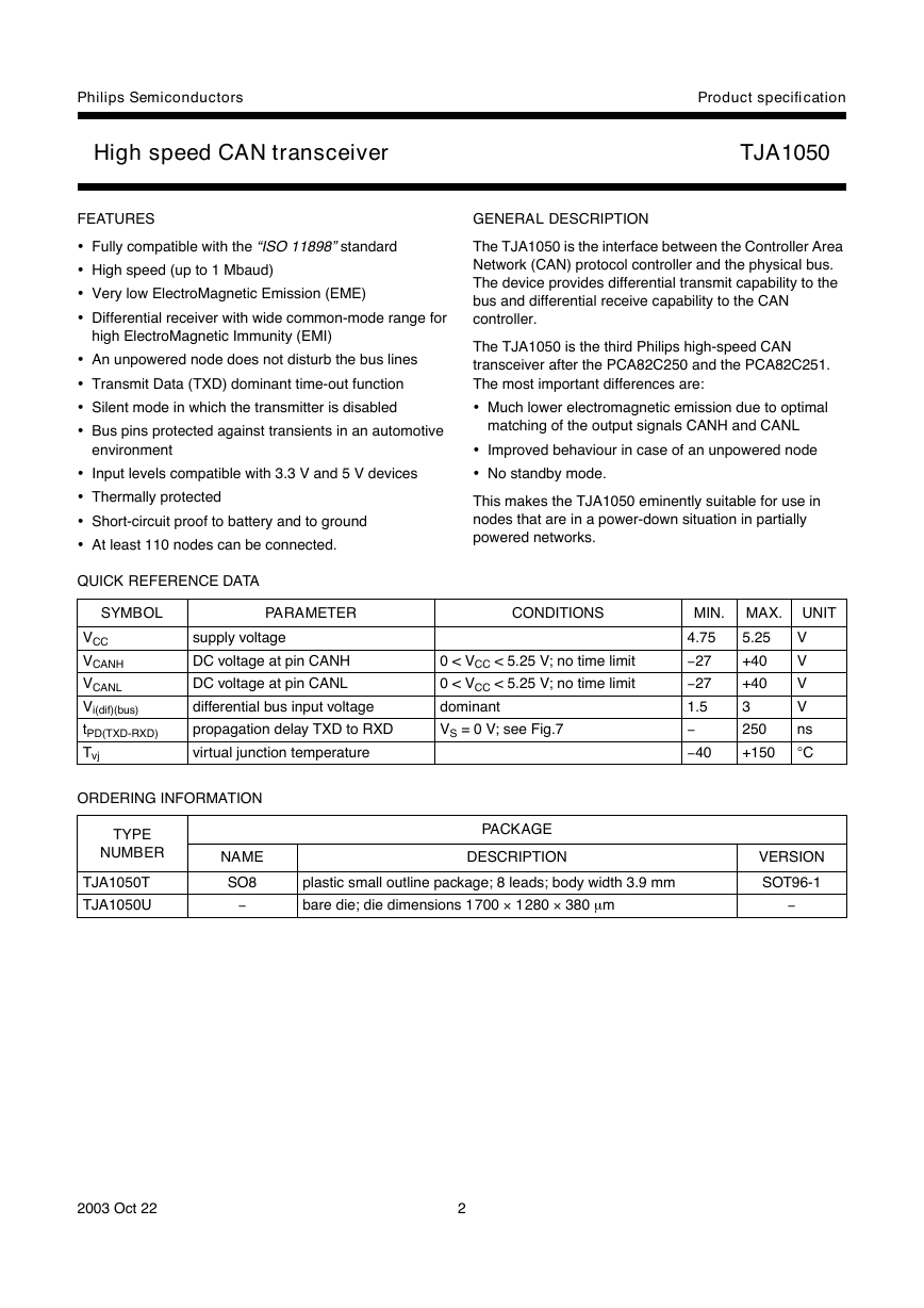
QUICK REFERENCE DATA
Product specification
TJA1050
GENERAL DESCRIPTION
The TJA1050 is the interface between the Controller Area
Network (CAN) protocol controller and the physical bus.
The device provides differential transmit capability to the
bus and differential receive capability to the CAN
controller.
The TJA1050 is the third Philips high-speed CAN
transceiver after the PCA82C250 and the PCA82C251.
The most important differences are:
• Much lower electromagnetic emission due to optimal
matching of the output signals CANH and CANL
• Improved behaviour in case of an unpowered node
• No standby mode.
This makes the TJA1050 eminently suitable for use in
nodes that are in a power-down situation in partially
powered networks.
SYMBOL
VCC
VCANH
VCANL
Vi(dif)(bus)
tPD(TXD-RXD)
Tvj
PARAMETER
CONDITIONS
supply voltage
DC voltage at pin CANH
DC voltage at pin CANL
differential bus input voltage
propagation delay TXD to RXD
virtual junction temperature
0 < VCC < 5.25 V; no time limit
0 < VCC < 5.25 V; no time limit
dominant
VS = 0 V; see Fig.7
- 40
MIN. MAX. UNIT
4.75
- 27
- 27
1.5
5.25
+40
+40
3
250
+150
V
V
V
V
ns
C
ORDERING INFORMATION
TYPE
NUMBER
TJA1050T
TJA1050U
NAME
SO8
PACKAGE
DESCRIPTION
plastic small outline package; 8 leads; body width 3.9 mm
bare die; die dimensions 1700 · 1280 · 380 m m
VERSION
SOT96-1
2003 Oct 22
2
-
-
-
�
VCC
3
TEMPERATURE
PROTECTION
DRIVER
Product specification
TJA1050
7
25
kW
25
kW
6
CANH
CANL
Philips Semiconductors
High speed CAN transceiver
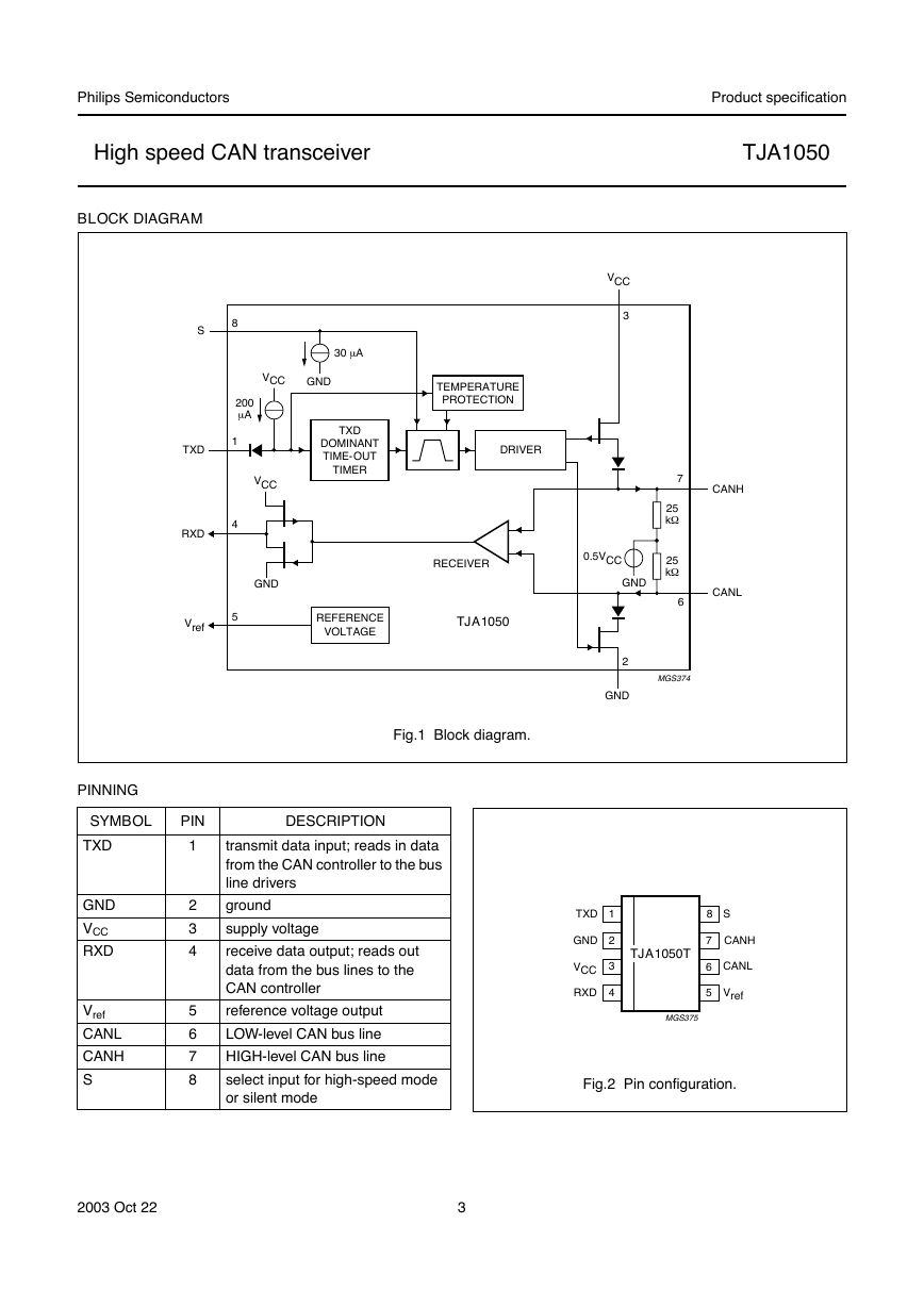
BLOCK DIAGRAM
handbook, full pagewidth
8
S
200
m A
30 m A
VCC
GND
TXD
DOMINANT
TIME-OUT
TIMER
1
4
5
VCC
GND
TXD
RXD
Vref
RECEIVER
0.5VCC
GND
REFERENCE
VOLTAGE
TJA1050
2
GND
MGS374
Fig.1 Block diagram.
PINNING
SYMBOL
TXD
PIN
1
GND
VCC
RXD
Vref
CANL
CANH
S
2
3
4
5
6
7
8
DESCRIPTION
transmit data input; reads in data
from the CAN controller to the bus
line drivers
ground
supply voltage
receive data output; reads out
data from the bus lines to the
CAN controller
reference voltage output
LOW-level CAN bus line
HIGH-level CAN bus line
select input for high-speed mode
or silent mode
2003 Oct 22
3
handbook, halfpage
TXD
GND
VCC
RXD
1
2
3
4
8
S
7
6
5
CANH
CANL
Vref
TJA1050T
MGS375
Fig.2 Pin configuration.
�
Philips Semiconductors
High speed CAN transceiver
Product specification
TJA1050
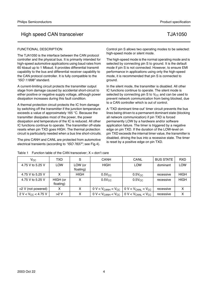
FUNCTIONAL DESCRIPTION
The TJA1050 is the interface between the CAN protocol
controller and the physical bus. It is primarily intended for
high-speed automotive applications using baud rates from
60 kbaud up to 1 Mbaud. It provides differential transmit
capability to the bus and differential receiver capability to
the CAN protocol controller. It is fully compatible to the
“ISO11898”standard.
A current-limiting circuit protects the transmitter output
stage from damage caused by accidental short-circuit to
either positive or negative supply voltage, although power
dissipation increases during this fault condition.
A thermal protection circuit protects the IC from damage
by switching off the transmitter if the junction temperature
exceeds a value of approximately 165 C. Because the
transmitter dissipates most of the power, the power
dissipation and temperature of the IC is reduced. All other
IC functions continue to operate. The transmitter off-state
resets when pin TXD goes HIGH. The thermal protection
circuit is particularly needed when a bus line short-circuits.
The pins CANH and CANL are protected from automotive
electrical transients (according to “ISO 7637”; see Fig.4).
Control pin S allows two operating modes to be selected:
high-speed mode or silent mode.
The high-speed mode is the normal operating mode and is
selected by connecting pin S to ground. It is the default
mode if pin S is not connected. However, to ensure EMI
performance in applications using only the high-speed
mode, it is recommended that pin S is connected to
ground.
In the silent mode, the transmitter is disabled. All other
IC functions continue to operate. The silent mode is
selected by connecting pin S to VCC and can be used to
prevent network communication from being blocked, due
to a CAN controller which is out of control.
A ‘TXD dominant time-out’ timer circuit prevents the bus
lines being driven to a permanent dominant state (blocking
all network communication) if pin TXD is forced
permanently LOW by a hardware and/or software
application failure. The timer is triggered by a negative
edge on pin TXD. If the duration of the LOW-level on
pin TXD exceeds the internal timer value, the transmitter is
disabled, driving the bus into a recessive state. The timer
is reset by a positive edge on pin TXD.
Table 1 Function table of the CAN transceiver; X = don’t care
VCC
4.75 V to 5.25 V
TXD
LOW
4.75 V to 5.25 V
4.75 V to 5.25 V
<2 V (not powered)
2 V < VCC < 4.75 V
X
HIGH (or
floating)
X
>2 V
S
LOW (or
floating)
HIGH
X
X
X
CANH
HIGH
0.5VCC
0.5VCC
CANL
LOW
0.5VCC
0.5VCC
BUS STATE
dominant
recessive
recessive
0 V < VCANH < VCC
0 V < VCANH < VCC
0 V < VCANL < VCC
0 V < VCANL < VCC
recessive
recessive
RXD
LOW
HIGH
HIGH
X
X
2003 Oct 22
4
�
Philips Semiconductors
High speed CAN transceiver
Product specification
TJA1050
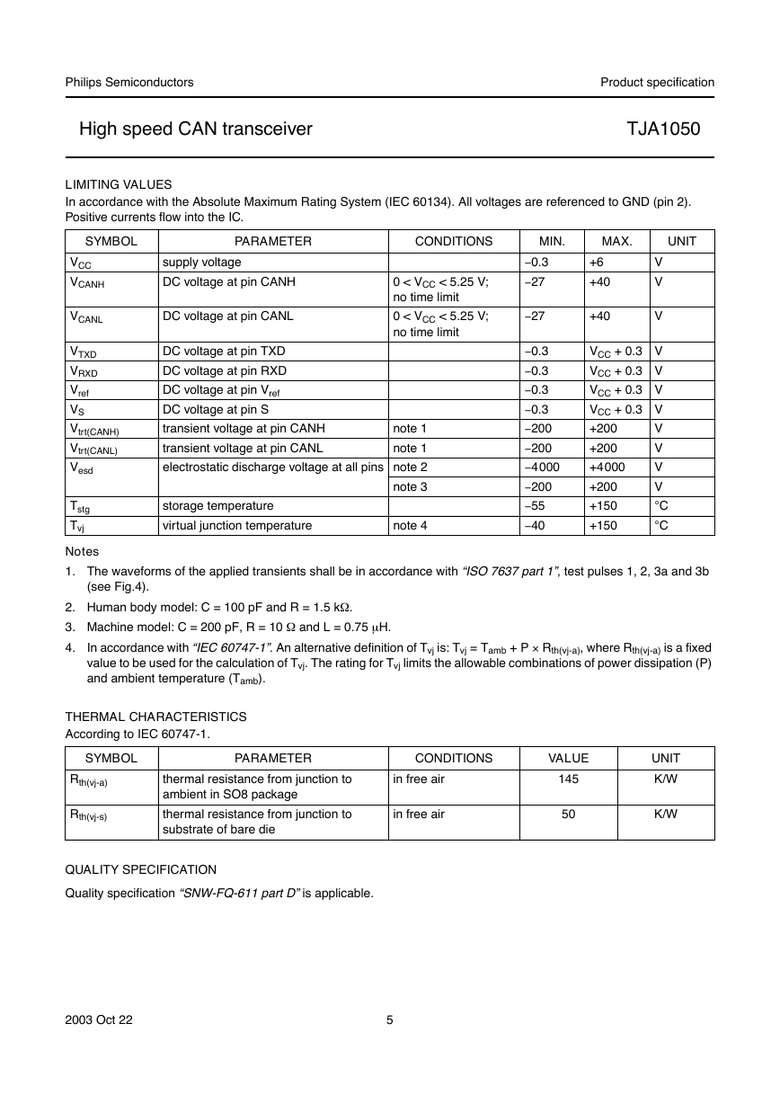
LIMITING VALUES
In accordance with the Absolute Maximum Rating System (IEC 60134). All voltages are referenced to GND (pin 2).
Positive currents flow into the IC.
SYMBOL
PARAMETER
CONDITIONS
MIN.
MAX.
UNIT
VCC
VCANH
VCANL
VTXD
VRXD
Vref
VS
Vtrt(CANH)
Vtrt(CANL)
Vesd
Tstg
Tvj
supply voltage
DC voltage at pin CANH
DC voltage at pin CANL
0 < VCC < 5.25 V;
no time limit
0 < VCC < 5.25 V;
no time limit
DC voltage at pin TXD
DC voltage at pin RXD
DC voltage at pin Vref
DC voltage at pin S
note 1
transient voltage at pin CANH
transient voltage at pin CANL
note 1
electrostatic discharge voltage at all pins note 2
note 3
storage temperature
virtual junction temperature
note 4
- 0.3
- 27
- 27
- 0.3
- 0.3
- 0.3
- 0.3
- 200
- 200
- 4000
- 200
- 55
- 40
+6
+40
+40
V
V
V
VCC + 0.3 V
VCC + 0.3 V
VCC + 0.3 V
VCC + 0.3 V
+200
V
V
+200
V
+4000
V
+200
C
+150
C
+150
Notes
1. The waveforms of the applied transients shall be in accordance with “ISO7637 part1”, test pulses 1, 2, 3a and 3b
(see Fig.4).
2. Human body model: C = 100 pF and R = 1.5 kW
3. Machine model: C = 200 pF, R = 10 W
4.
.
and L = 0.75 m H.
In accordance with “IEC60747-1”. An alternative definition of Tvj is: Tvj = Tamb + P · Rth(vj-a), where Rth(vj-a) is a fixed
value to be used for the calculation of Tvj. The rating for Tvj limits the allowable combinations of power dissipation (P)
and ambient temperature (Tamb).
THERMAL CHARACTERISTICS
According to IEC 60747-1.
SYMBOL
PARAMETER
CONDITIONS
VALUE
Rth(vj-a)
Rth(vj-s)
thermal resistance from junction to
ambient in SO8 package
thermal resistance from junction to
substrate of bare die
in free air
in free air
145
50
UNIT
K/W
K/W
QUALITY SPECIFICATION
Quality specification “SNW-FQ-611partD” is applicable.
2003 Oct 22
5
�
Philips Semiconductors
High speed CAN transceiver
Product specification
TJA1050
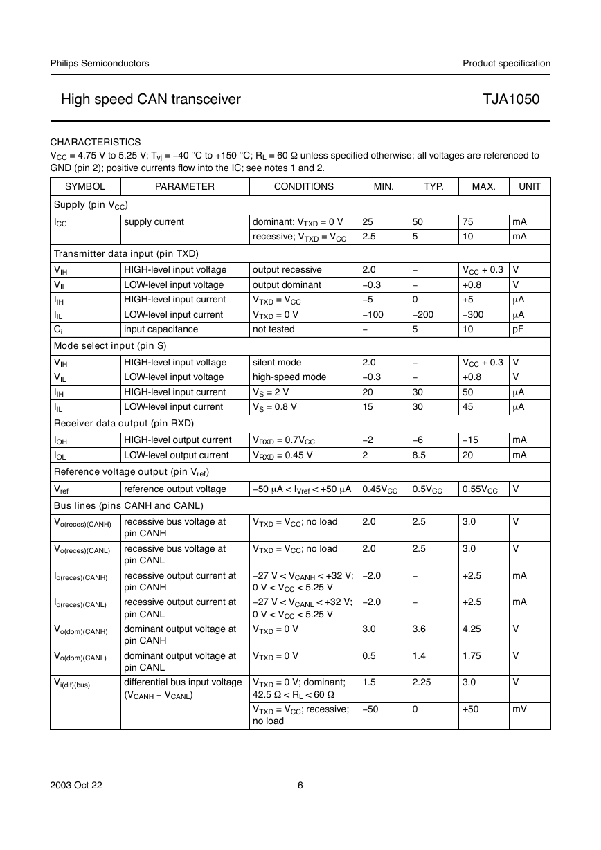
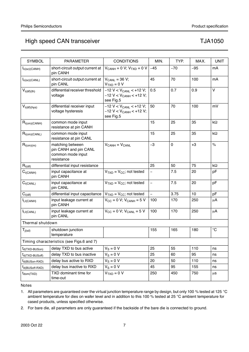
CHARACTERISTICS
VCC = 4.75 V to 5.25 V; Tvj = - 40 C to +150 C; RL = 60 W
GND (pin 2); positive currents flow into the IC; see notes 1 and 2.
unless specified otherwise; all voltages are referenced to
SYMBOL
PARAMETER
CONDITIONS
MIN.
TYP.
MAX.
UNIT
Supply (pin VCC)
ICC
supply current
dominant; VTXD = 0 V
recessive; VTXD = VCC
25
2.5
50
5
75
10
mA
mA
HIGH-level input voltage
LOW-level input voltage
HIGH-level input current
LOW-level input current
input capacitance
Transmitter data input (pin TXD)
VIH
VIL
IIH
IIL
Ci
Mode select input (pin S)
VIH
VIL
IIH
IIL
Receiver data output (pin RXD)
IOH
IOL
Reference voltage output (pin Vref)
Vref
Bus lines (pins CANH and CANL)
Vo(reces)(CANH)
HIGH-level input voltage
LOW-level input voltage
HIGH-level input current
LOW-level input current
HIGH-level output current
LOW-level output current
reference output voltage
Vo(reces)(CANL)
Io(reces)(CANH)
Io(reces)(CANL)
Vo(dom)(CANH)
Vo(dom)(CANL)
Vi(dif)(bus)
recessive bus voltage at
pin CANH
recessive bus voltage at
pin CANL
recessive output current at
pin CANH
recessive output current at
pin CANL
dominant output voltage at
pin CANH
dominant output voltage at
pin CANL
differential bus input voltage
(VCANH - VCANL)
output recessive
output dominant
VTXD = VCC
VTXD = 0 V
not tested
silent mode
high-speed mode
VS = 2 V
VS = 0.8 V
VRXD = 0.7VCC
VRXD = 0.45 V
2.0
- 0.3
- 5
- 100
2.0
- 0.3
20
15
- 2
2
0
- 200
5
30
30
- 6
8.5
VCC + 0.3 V
+0.8
V
m A
+5
m A
- 300
10
pF
VCC + 0.3 V
+0.8
V
m A
50
m A
45
- 15
20
- 50 m A < IVref < +50 m A 0.45VCC
0.5VCC
0.55VCC
VTXD = VCC; no load
VTXD = VCC; no load
- 27 V < VCANH < +32 V;
0 V < VCC < 5.25 V
- 27 V < VCANL < +32 V;
0 V < VCC < 5.25 V
VTXD = 0 V
VTXD = 0 V
VTXD = 0 V; dominant;
42.5 W < RL < 60 W
VTXD = VCC; recessive;
no load
2.0
2.0
- 2.0
- 2.0
3.0
0.5
1.5
- 50
2.5
2.5
3.6
1.4
2.25
0
3.0
3.0
+2.5
+2.5
4.25
1.75
3.0
+50
mA
mA
V
V
V
mA
mA
V
V
V
mV
2003 Oct 22
6
-
-
-
-
-
-
-
�
Philips Semiconductors
High speed CAN transceiver
Product specification
TJA1050
PARAMETER
CONDITIONS
MIN.
TYP.
MAX.
UNIT
- 95
100
0.9
mA
mA
V
100
mV
35
35
+3
75
20
20
10
250
250
kW
kW
%
kW
pF
pF
pF
m A
m A
C
ns
ns
ns
ns
m s
SYMBOL
Io(sc)(CANH)
Io(sc)(CANL)
Vi(dif)(th)
short-circuit output current at
pin CANH
short-circuit output current at
pin CANL
differential receiver threshold
voltage
Vi(dif)(hys)
differential receiver input
voltage hysteresis
VCANH = 0 V; VTXD = 0 V - 45
VCANL = 36 V;
VTXD = 0 V
- 12 V < VCANL < +12 V;
- 12 V < VCANH < +12 V;
see Fig.5
- 12 V < VCANL < +12 V;
- 12 V < VCANH < +12 V;
see Fig.5
Ri(cm)(CANH)
Ri(cm)(CANL)
Ri(cm)(m)
Ri(dif)
Ci(CANH)
Ci(CANL)
Ci(dif)
ILI(CANH)
ILI(CANL)
VCANH = VCANL
common mode input
resistance at pin CANH
common mode input
resistance at pin CANL
matching between
pin CANH and pin CANL
common mode input
resistance
differential input resistance
input capacitance at
pin CANH
input capacitance at
pin CANL
differential input capacitance VTXD = VCC; not tested
input leakage current at
pin CANH
input leakage current at
pin CANL
VTXD = VCC; not tested
VTXD = VCC; not tested
VCC = 0 V; VCANH = 5 V 100
VCC = 0 V; VCANL = 5 V 100
45
0.5
50
15
15
- 3
25
- 70
70
0.7
70
25
25
0
50
7.5
7.5
3.75
170
170
Thermal shutdown
Tj(sd)
shutdown junction
temperature
Timing characteristics (see Figs.6 and 7)
td(TXD-BUSon)
td(TXD-BUSoff)
td(BUSon-RXD)
td(BUSoff-RXD)
tdom(TXD)
delay TXD to bus active
delay TXD to bus inactive
delay bus active to RXD
delay bus inactive to RXD
TXD dominant time for
time-out
VS = 0 V
VS = 0 V
VS = 0 V
VS = 0 V
VTXD = 0 V
155
165
180
25
25
20
45
250
55
60
50
95
450
110
95
110
155
750
Notes
1. All parameters are guaranteed over the virtual junction temperature range by design, but only 100 % tested at 125 C
ambient temperature for dies on wafer level and in addition to this 100 % tested at 25 C ambient temperature for
cased products, unless specified otherwise.
2. For bare die, all parameters are only guaranteed if the backside of the bare die is connected to ground.
2003 Oct 22
7
-
-
-
�
Product specification
TJA1050
Philips Semiconductors
High speed CAN transceiver
APPLICATION AND TEST INFORMATION
handbook, full pagewidth
+5 V
TX0
SJA1000
CAN
CONTROLLER
RX0
MICRO-
CONTROLLER
100
nF
VCC
3
TJA1050
2
8
GND S
TXD
Vref
RXD
1
5
4
47 nF
60 W
60 W
CANH
CANL
7
6
CAN
BUS LINE
60 W
60 W
47 nF
MGS380
Fig.3 Application information.
handbook, full pagewidth
+5 V
100
nF
VCC
3
TJA1050
2
8
GND S
7
6
TXD
Vref
RXD
1
5
4
15 pF
CANH
1 nF
CANL
1 nF
TRANSIENT
GENERATOR
MGS379
The waveforms of the applied transients shall be in accordance with “ISO 7637 part 1”, test pulses 1, 2, 3a and 3b.
Fig.4 Test circuit for automotive transients.
2003 Oct 22
8
�


 2023年江西萍乡中考道德与法治真题及答案.doc
 2012年重庆南川中考生物真题及答案.doc
 2013年江西师范大学地理学综合及文艺理论基础考研真题.doc
 2020年四川甘孜小升初语文真题及答案I卷.doc
 2020年注册岩土工程师专业基础考试真题及答案.doc
 2023-2024学年福建省厦门市九年级上学期数学月考试题及答案.doc
 2021-2022学年辽宁省沈阳市大东区九年级上学期语文期末试题及答案.doc
 2022-2023学年北京东城区初三第一学期物理期末试卷及答案.doc
 2018上半年江西教师资格初中地理学科知识与教学能力真题及答案.doc
 2012年河北国家公务员申论考试真题及答案-省级.doc
 2020-2021学年江苏省扬州市江都区邵樊片九年级上学期数学第一次质量检测试题及答案.doc
 2022下半年黑龙江教师资格证中学综合素质真题及答案.doc