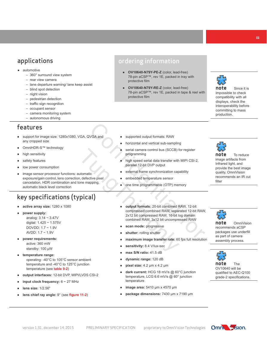
applications
features
key specifications (typical)
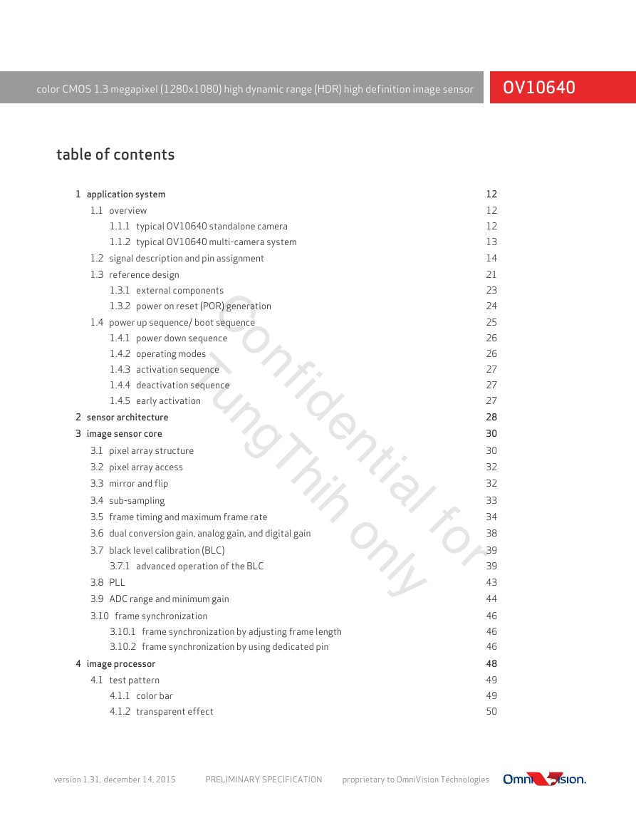
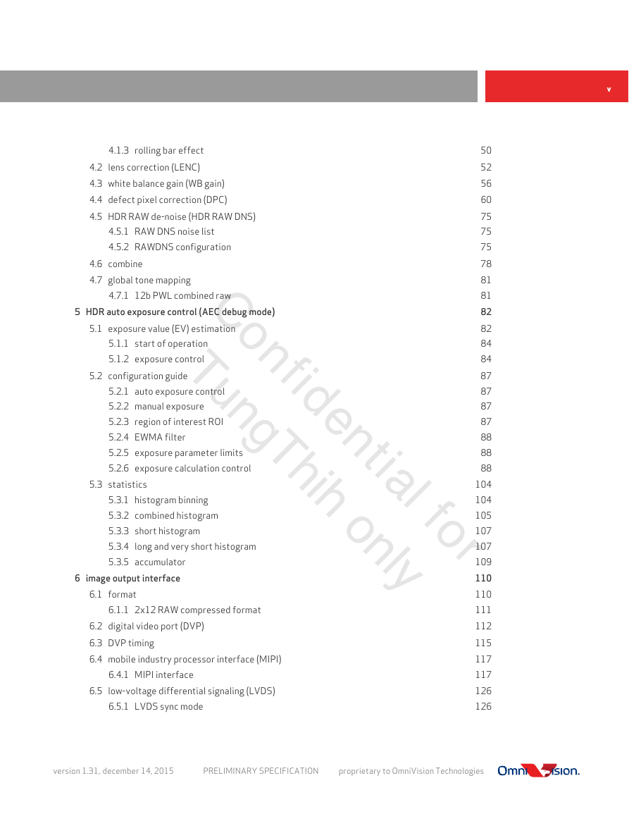
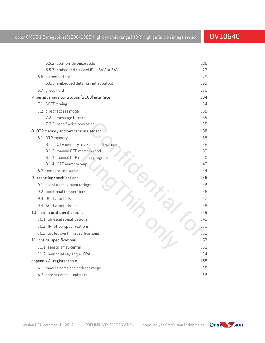
table of contents
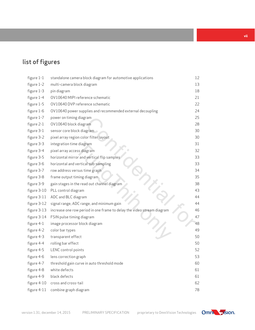
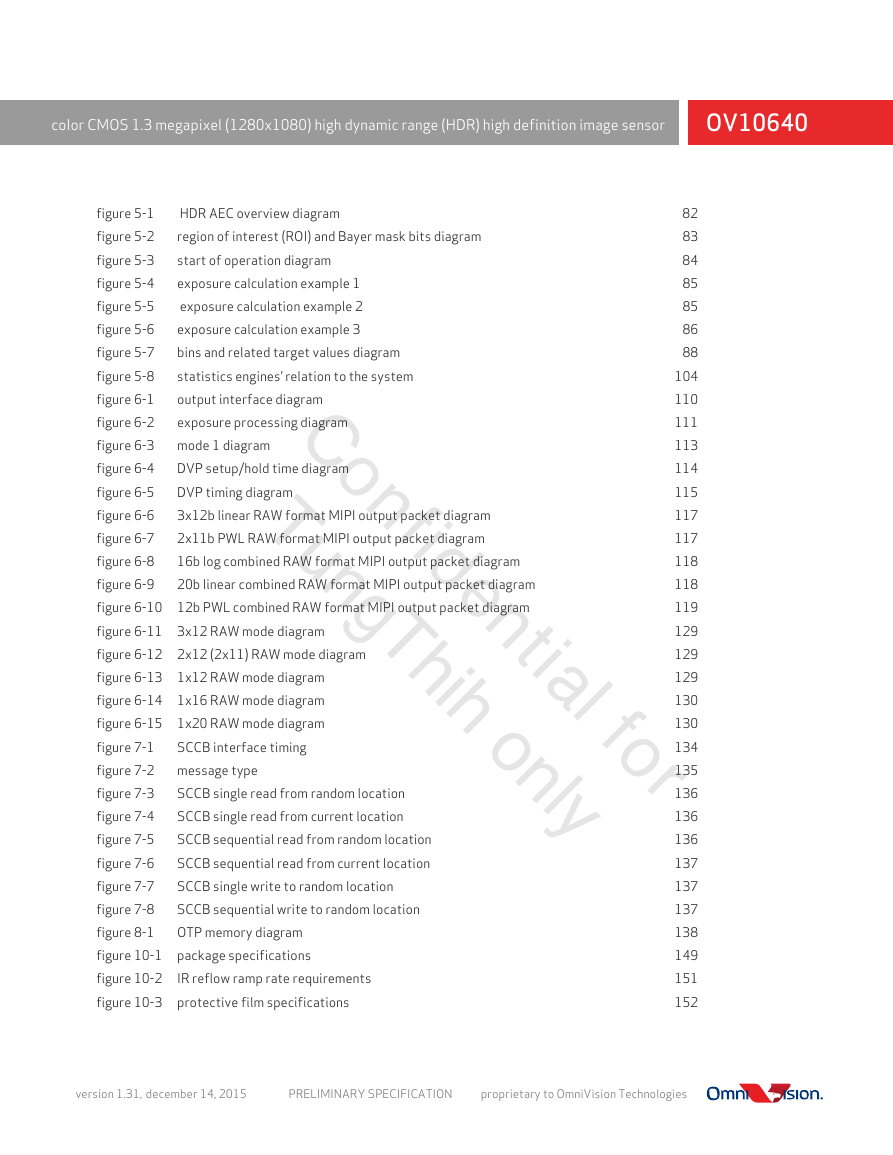
list of figures
list of tables
1 application system
1.1 overview
1.1.1 typical OV10640 standalone camera
figure 1-1 standalone camera block diagram for automotive applications
1.1.2 typical OV10640 multi-camera system
figure 1-2 multi-camera block diagram
1.2 signal description and pin assignment
table 1-1 signal descriptions (sheet 1 of 3)
table 1-2 pin states under various conditions
figure 1-3 pin diagram
table 1-3 pad equivalent circuit (sheet 1 of 2)
1.3 reference design
figure 1-4 OV10640 MIPI reference schematic
figure 1-5 OV10640 DVP reference schematic
1.3.1 external components
table 1-4 power supplies
figure 1-6 OV10640 power supplies and recommended external decoupling
1.3.2 power on reset (POR) generation
1.4 power up sequence/ boot sequence
figure 1-7 power on timing diagram
table 1-5 power on timing
1.4.1 power down sequence
1.4.2 operating modes
1.4.3 activation sequence
1.4.4 deactivation sequence
1.4.5 early activation
2 sensor architecture
figure 2-1 OV10640 block diagram
3 image sensor core
figure 3-1 sensor core block diagram
3.1 pixel array structure
figure 3-2 pixel array region color filter layout
figure 3-3 integration time diagram
3.2 pixel array access
figure 3-4 pixel array access diagram
3.3 mirror and flip
figure 3-5 horizontal mirror and vertical flip samples
3.4 sub-sampling
figure 3-6 horizontal and vertical sub-sampling
3.5 frame timing and maximum frame rate
figure 3-7 row address versus time graph
figure 3-8 frame output timing diagram
table 3-1 supported output formats and frame rates (sheet 1 of 2)
table 3-2 timing control registers (sheet 1 of 2)
3.6 dual conversion gain, analog gain, and digital gain
figure 3-9 gain stages in the read out channel diagram
table 3-3 gain registers (sheet 1 of 2)
3.7 black level calibration (BLC)
3.7.1 advanced operation of the BLC
table 3-4 BLC control registers (sheet 1 of 3)
3.8 PLL
figure 3-10 PLL control diagram
table 3-5 PLL control registers
3.9 ADC range and minimum gain
figure 3-11 ADC and BLC diagram
figure 3-12 signal range, ADC range, and minimum gain
3.10 frame synchronization
3.10.1 frame synchronization by adjusting frame length
figure 3-13 increase one row period in one frame to delay the video stream diagram
3.10.2 frame synchronization by using dedicated pin
figure 3-14 FSIN pulse timing diagram
4 image processor
figure 4-1 image processor block diagram
4.1 test pattern
4.1.1 color bar
figure 4-2 color bar types
4.1.2 transparent effect
figure 4-3 transparent effect
4.1.3 rolling bar effect
figure 4-4 rolling bar effect
table 4-1 test pattern control registers
4.2 lens correction (LENC)
figure 4-5 LENC control points
figure 4-6 lens correction graph
table 4-2 LENC control registers (sheet 1 of 2)
4.3 white balance gain (WB gain)
table 4-3 WB control registers (sheet 1 of 4)
4.4 defect pixel correction (DPC)
figure 4-7 threshold gain curve in auto threshold mode
figure 4-8 white defects
figure 4-9 black defects
figure 4-10 cross and cross-tail
table 4-4 DPC control registers (sheet 1 of 12)
4.5 HDR RAW de-noise (HDR RAW DNS)
4.5.1 RAW DNS noise list
4.5.2 RAWDNS configuration
table 4-5 HDR_RAW control registers (sheet 1 of 3)
4.6 combine
figure 4-11 combine graph diagram
table 4-6 combine control registers (sheet 1 of 2)
4.7 global tone mapping
4.7.1 12b PWL combined raw
5 HDR auto exposure control (AEC debug mode)
5.1 exposure value (EV) estimation
figure 5-1 HDR AEC overview diagram
figure 5-2 region of interest (ROI) and Bayer mask bits diagram
5.1.1 start of operation
figure 5-3 start of operation diagram
5.1.2 exposure control
figure 5-4 exposure calculation example 1
figure 5-5 exposure calculation example 2
figure 5-6 exposure calculation example 3
5.2 configuration guide
5.2.1 auto exposure control
5.2.2 manual exposure
5.2.3 region of interest ROI
figure 5-7 bins and related target values diagram
5.2.4 EWMA filter
5.2.5 exposure parameter limits
5.2.6 exposure calculation control
table 5-1 HDR_AEC control registers (sheet 1 of 15)
5.3 statistics
5.3.1 histogram binning
figure 5-8 statistics engines’ relation to the system
5.3.2 combined histogram
table 5-2 code range per bin with 20-bit data (sheet 1 of 2)
table 5-3 code range per bin with 16-bit data
table 5-4 code range per bin with 12-bit data
5.3.3 short histogram
5.3.4 long and very short histogram
table 5-5 bin scopes for aec_longest (L) and aec_shortest (VS)
5.3.5 accumulator
6 image output interface
figure 6-1 output interface diagram
6.1 format
table 6-1 format control register
6.1.1 2x12 RAW compressed format
figure 6-2 exposure processing diagram
6.2 digital video port (DVP)
table 6-2 output formats
figure 6-3 mode 1 diagram
figure 6-4 DVP setup/hold time diagram
table 6-3 DVP setup/hold time
6.3 DVP timing
figure 6-5 DVP timing diagram
table 6-4 DVP control registers (sheet 1 of 2)
6.4 mobile industry processor interface (MIPI)
6.4.1 MIPI interface
figure 6-6 3x12b linear RAW format MIPI output packet diagram
figure 6-7 2x11b PWL RAW format MIPI output packet diagram
figure 6-8 16b log combined RAW format MIPI output packet diagram
figure 6-9 20b linear combined RAW format MIPI output packet diagram
figure 6-10 12b PWL combined RAW format MIPI output packet diagram
table 6-5 MIPI control registers (sheet 1 of 7)
6.5 low-voltage differential signaling (LVDS)
6.5.1 LVDS sync mode
6.5.2 split synchronize code
6.5.3 embedded channel ID in SAV or EAV
table 6-6 LVDS registers (sheet 1 of 2)
6.6 embedded data
6.6.1 embedded data format at output
figure 6-11 3x12 RAW mode diagram
figure 6-12 2x12 (2x11) RAW mode diagram
figure 6-13 1x12 RAW mode diagram
figure 6-14 1x16 RAW mode diagram
figure 6-15 1x20 RAW mode diagram
6.7 group hold
table 6-7 group hold control registers (sheet 1 of 2)
7 serial camera control bus (SCCB) interface
7.1 SCCB timing
figure 7-1 SCCB interface timing
table 7-1 SCCB interface timing specifications
7.2 direct access mode
7.2.1 message format
figure 7-2 message type
7.2.2 read / write operation
figure 7-3 SCCB single read from random location
figure 7-4 SCCB single read from current location
figure 7-5 SCCB sequential read from random location
figure 7-6 SCCB sequential read from current location
figure 7-7 SCCB single write to random location
figure 7-8 SCCB sequential write to random location
8 OTP memory and temperature sensor
8.1 OTP memory
figure 8-1 OTP memory diagram
8.1.1 OTP memory access considerations
8.1.2 manual OTP memory read
8.1.3 manual OTP memory program
8.1.4 OTP memory map
table 8-1 OTP memory structure
table 8-2 OTP control registers (sheet 1 of 3)
8.2 temperature sensor
table 8-3 temperature control registers
9 operating specifications
9.1 absolute maximum ratings
table 9-1 absolute maximum ratings
9.2 functional temperature
table 9-2 functional temperature
9.3 DC characteristics
table 9-3 DC characteristics (-40°C < TJ < 125°C)
9.4 AC characteristics
table 9-4 AC characteristics (TA = 25°C, VDD-A = 3.3V, VDD-IO = 1.8V)
table 9-5 timing characteristics
10 mechanical specifications
10.1 physical specifications
figure 10-1 package specifications
table 10-1 package dimensions (sheet 1 of 2)
10.2 IR reflow specifications
figure 10-2 IR reflow ramp rate requirements
table 10-2 reflow conditions
10.3 protective film specifications
figure 10-3 protective film specifications
11 optical specifications
11.1 sensor array center
figure 11-1 sensor array center
11.2 lens chief ray angle (CRA)
figure 11-2 chief ray angle (CRA)
table 11-1 CRA versus image height plot
appendix A register table
A.1 module name and address range
A.2 sensor control registers
revision history


 2023年江西萍乡中考道德与法治真题及答案.doc
 2012年重庆南川中考生物真题及答案.doc
 2013年江西师范大学地理学综合及文艺理论基础考研真题.doc
 2020年四川甘孜小升初语文真题及答案I卷.doc
 2020年注册岩土工程师专业基础考试真题及答案.doc
 2023-2024学年福建省厦门市九年级上学期数学月考试题及答案.doc
 2021-2022学年辽宁省沈阳市大东区九年级上学期语文期末试题及答案.doc
 2022-2023学年北京东城区初三第一学期物理期末试卷及答案.doc
 2018上半年江西教师资格初中地理学科知识与教学能力真题及答案.doc
 2012年河北国家公务员申论考试真题及答案-省级.doc
 2020-2021学年江苏省扬州市江都区邵樊片九年级上学期数学第一次质量检测试题及答案.doc
 2022下半年黑龙江教师资格证中学综合素质真题及答案.doc