Product SPEC Product: PL-2303
Data Sheet for PL2303 USB-to-RS232 Bridge
Features
¤ Full compliance with the USB Specification v1.1
¤ Support the RS232 Serial interface
¤ Support automatic handshake mode
¤ Over 1Mbps transfer rate
¤ Support remote wake-up and power management
¤ Dual data buffers for upstream and downstream data flow
¤ Support default ROM or external EEPROM for device configuration
¤ On chip USB transceiver
¤ On chip crystal oscillator running at 12M Hz
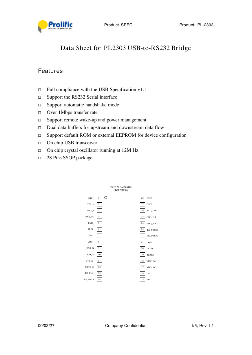
¤ 28 Pins SSOP package
SSOP 28 PACKAGE
(TOP VIEW)
TXD
DTR_N
RTS_N
VDD_232
RXD
RI_N
GND
VDD
DSR_N
DCD_N
CTS_N
SHTD_N
EE_CLK
EE_DATA
1
2
3
4
5
6
7
8
9
10
11
12
13
14
28
OSC2
27
OSC1
26
25
24
23
22
21
20
19
PLL_TEST
GND_PLL
VDD_PLL
LD_MODE
TRI_MODE
GND
VDD
RESET
18
GND_3V3
17
VDD_3V3
16 DM
15
DP
00/03/27
Company Confidential
1/5; Rev 1.1
�
Product SPEC Product: PL-2303
1. Introduction
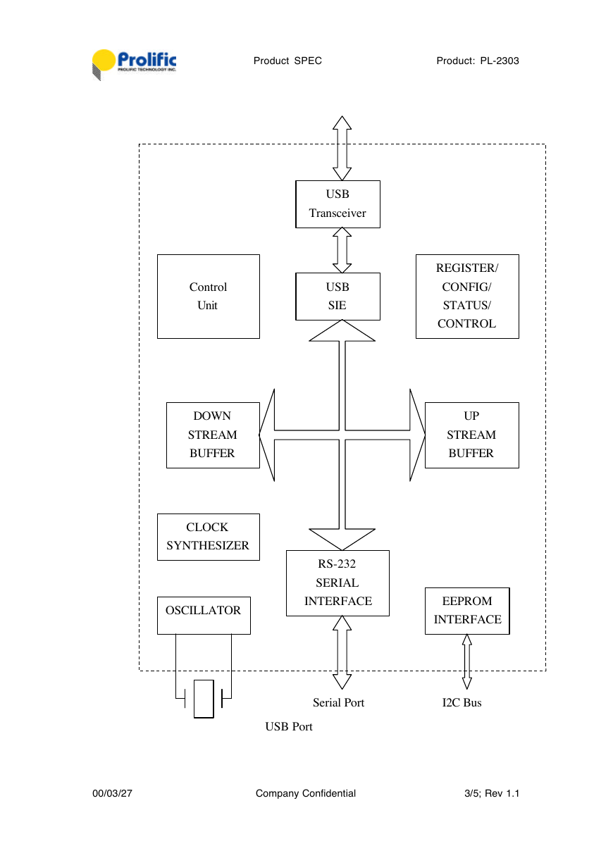
The PL-2303 operates as a bridge between one USB port and one standard RS232
Serial port. Figure 1 in the following page shows its interface and internal block
diagram.
The two large on-chip buffers accommodate the data flow from two different buses.
The USB bulk-type data is adopted for maximum data transfer. Automatic handshake
is supported at the Serial port. With these, a much higher baud rate can be achieved
compared to the legacy UART controller.
This device is also compliant with USB power management and remote wakeup
scheme. Only minimum power is consumed from the host during suspend. By
integrating all the functions into the SSOP-28 package, this chip is suitable for cable
embedding. Users just simply hook the cable into PC or hub’s USB port, then they
can connect to any RS-232 devices.
00/03/27
Company Confidential
2/5; Rev 1.1
�
Product SPEC Product: PL-2303
USB
Transceiver
Control
Unit
USB
SIE
DOWN
STREAM
BUFFER
CLOCK
SYNTHESIZER
OSCILLATOR
REGISTER/
CONFIG/
STATUS/
CONTROL
UP
STREAM
BUFFER
RS-232
SERIAL
INTERFACE
EEPROM
INTERFACE
Serial Port
I2C Bus
USB Port
00/03/27
Company Confidential
3/5; Rev 1.1
�
Product SPEC Product: PL-2303
Figure 1. USB-Serial Block Diagram
2. Pin Description
I – Input signal
O – Output signal
I/O – Bi-directional signal
I* – 5V TTL Schmitt Input signal
O* – 3.3V tri-state output
P – Power/Ground
TXD
Name
Pin
No.
1
2 DTR_N
3
RTS_N
4 VDD_232
RXD
5
RI_N
6
7 GND
8 VDD
9 DSR_N
10 DCD_N
11 CTS_N
12
SHTD_N
13 EE_CLK
14 EE_DATA
15 DP
16 DM
17 VDD_3V3
18 GND_3V3
19 RESET
20 VDD
21 GND
22 TRI_MODE
23 LD_MODE
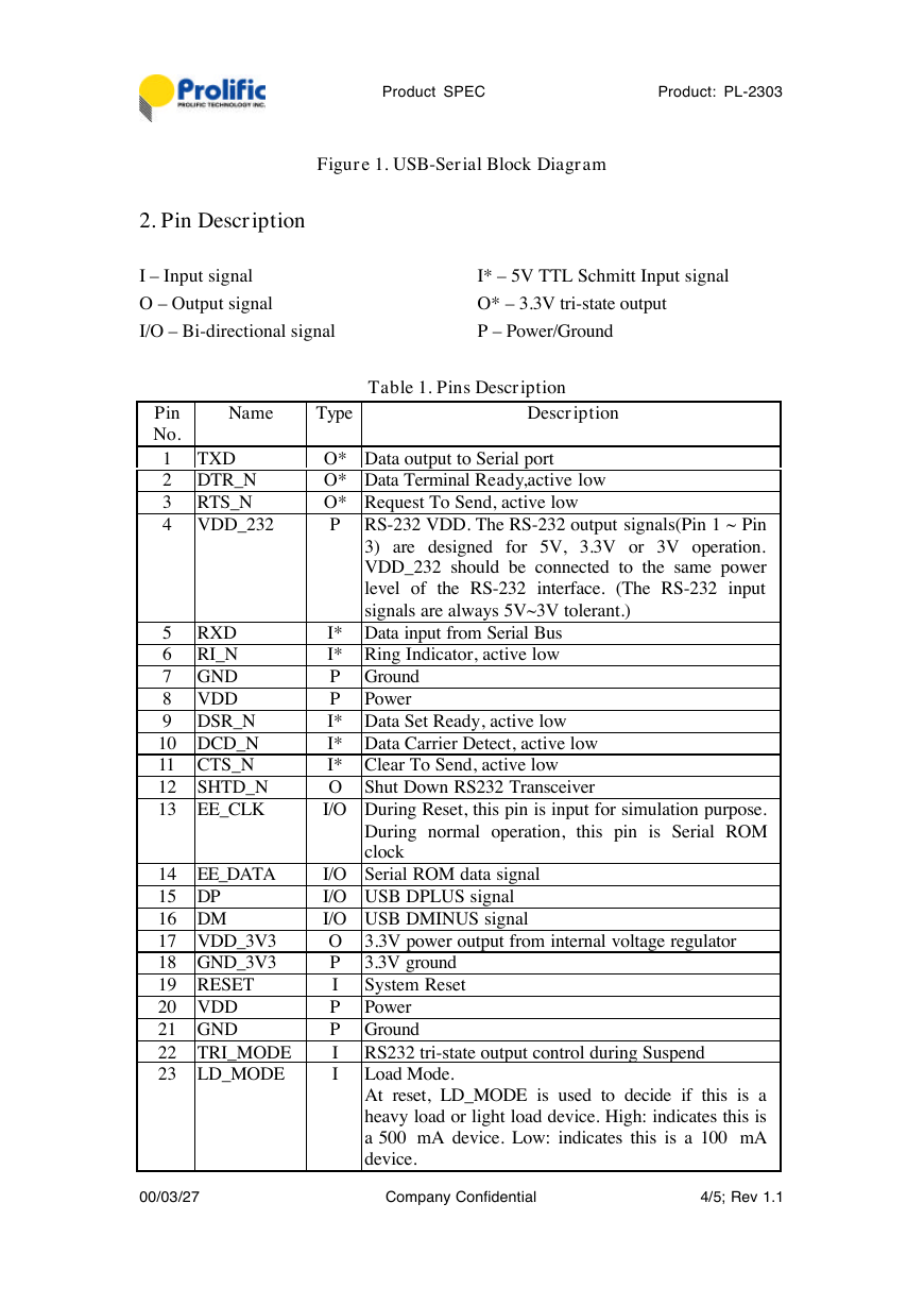
Table 1. Pins Description
Type
Description
O* Data output to Serial port
O* Data Terminal Ready,active low
O* Request To Send, active low
P RS-232 VDD. The RS-232 output signals(Pin 1 ~ Pin
3) are designed for 5V, 3.3V or 3V operation.
VDD_232 should be connected to the same power
level of the RS-232 interface. (The RS-232 input
signals are always 5V~3V tolerant.)
I* Data input from Serial Bus
I* Ring Indicator, active low
P Ground
P
Power
I* Data Set Ready, active low
I* Data Carrier Detect, active low
I* Clear To Send, active low
O Shut Down RS232 Transceiver
I/O During Reset, this pin is input for simulation purpose.
During normal operation, this pin is Serial ROM
clock
I/O Serial ROM data signal
I/O USB DPLUS signal
I/O USB DMINUS signal
O 3.3V power output from internal voltage regulator
3.3V ground
P
System Reset
I
P
Power
P Ground
I
I
RS232 tri-state output control during Suspend
Load Mode.
At reset, LD_MODE is used to decide if this is a
heavy load or light load device. High: indicates this is
a 500 mA device. Low: indicates this is a 100 mA
device.
00/03/27
Company Confidential
4/5; Rev 1.1
�
Product SPEC Product: PL-2303
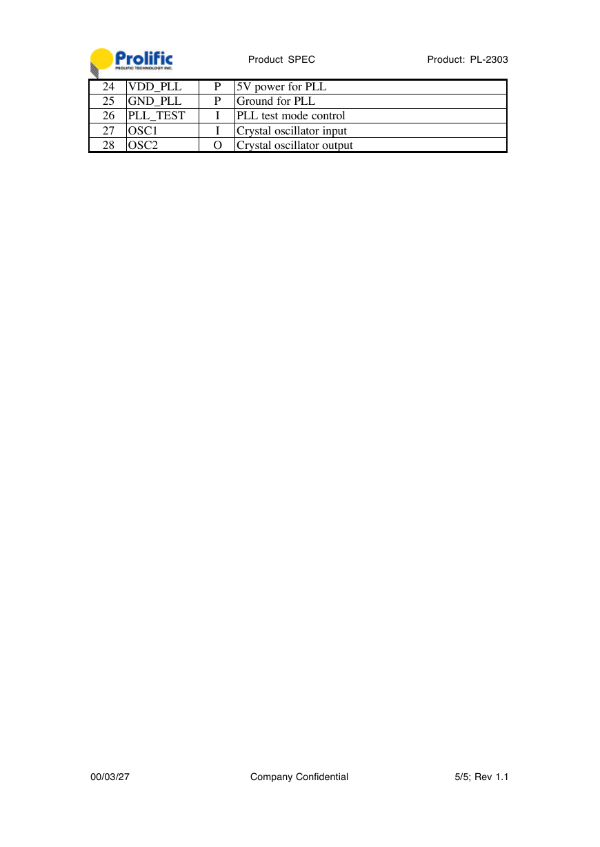
24 VDD_PLL
25 GND_PLL
26
PLL_TEST
27 OSC1
28 OSC2
5V power for PLL
P
P Ground for PLL
I
PLL test mode control
I
Crystal oscillator input
O Crystal oscillator output
00/03/27
Company Confidential
5/5; Rev 1.1
�


 2023年江西萍乡中考道德与法治真题及答案.doc
 2012年重庆南川中考生物真题及答案.doc
 2013年江西师范大学地理学综合及文艺理论基础考研真题.doc
 2020年四川甘孜小升初语文真题及答案I卷.doc
 2020年注册岩土工程师专业基础考试真题及答案.doc
 2023-2024学年福建省厦门市九年级上学期数学月考试题及答案.doc
 2021-2022学年辽宁省沈阳市大东区九年级上学期语文期末试题及答案.doc
 2022-2023学年北京东城区初三第一学期物理期末试卷及答案.doc
 2018上半年江西教师资格初中地理学科知识与教学能力真题及答案.doc
 2012年河北国家公务员申论考试真题及答案-省级.doc
 2020-2021学年江苏省扬州市江都区邵樊片九年级上学期数学第一次质量检测试题及答案.doc
 2022下半年黑龙江教师资格证中学综合素质真题及答案.doc