logo资料库

13.56mhz_天线设计.pdf

第1页 / 共50页
第2页 / 共50页
第3页 / 共50页
第4页 / 共50页
第5页 / 共50页
第6页 / 共50页
第7页 / 共50页
第8页 / 共50页
资料共50页,剩余部分请下载后查看
Introduction
Review of a Basic Theory for RFID antenna Design
Current and Magnetic Fields
FIGURE 1: Calculation of magnetic field B at location P due to current I on a straight conducting...
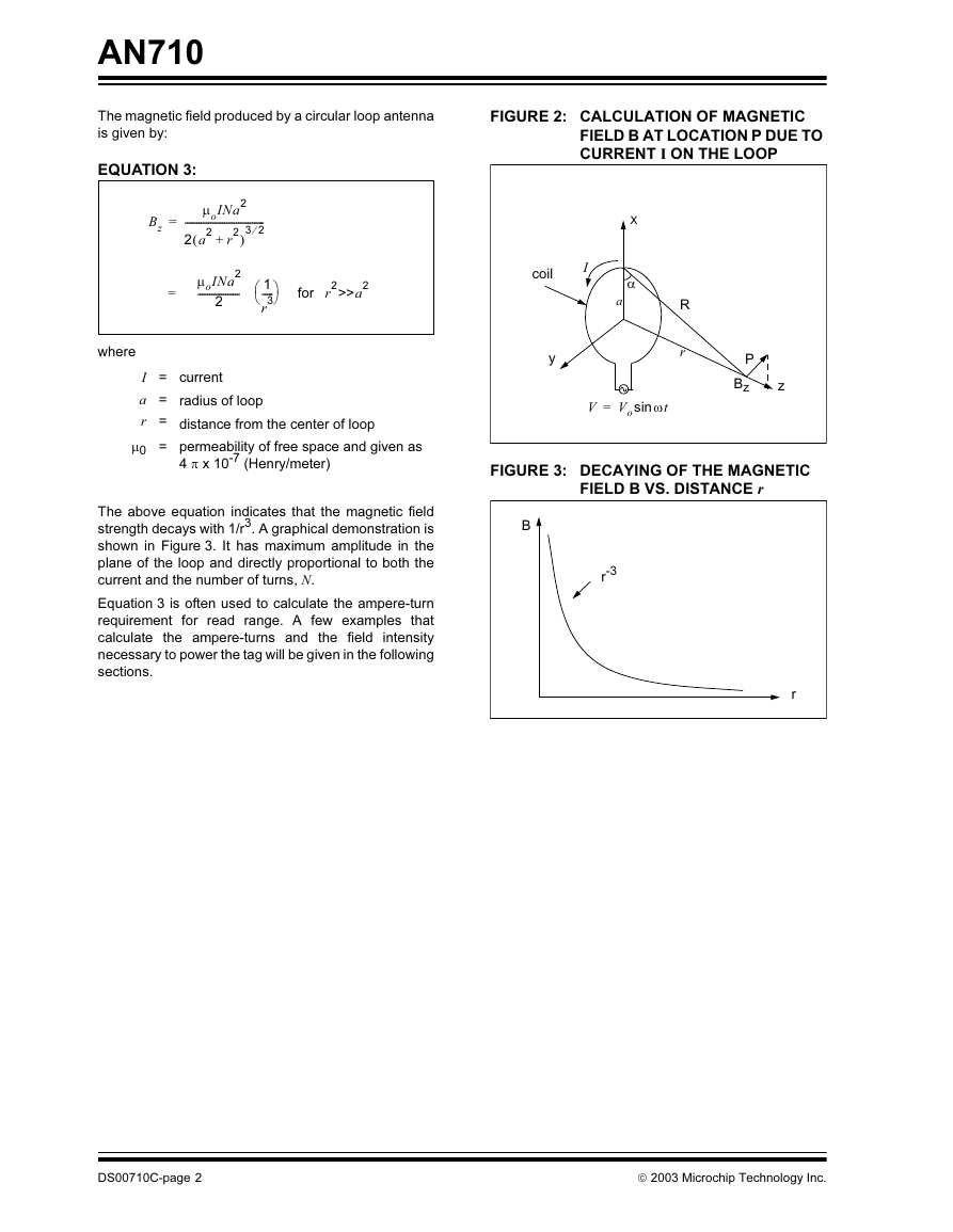
FIGURE 2: Calculation of magnetic field B at location P due to current I on the loop
FIGURE 3: Decaying of the magnetic field B vs. distance r
Induced Voltage in an Antenna Coil
FIGURE 4: A basic configuration of reader and tag antennas in RFID applications
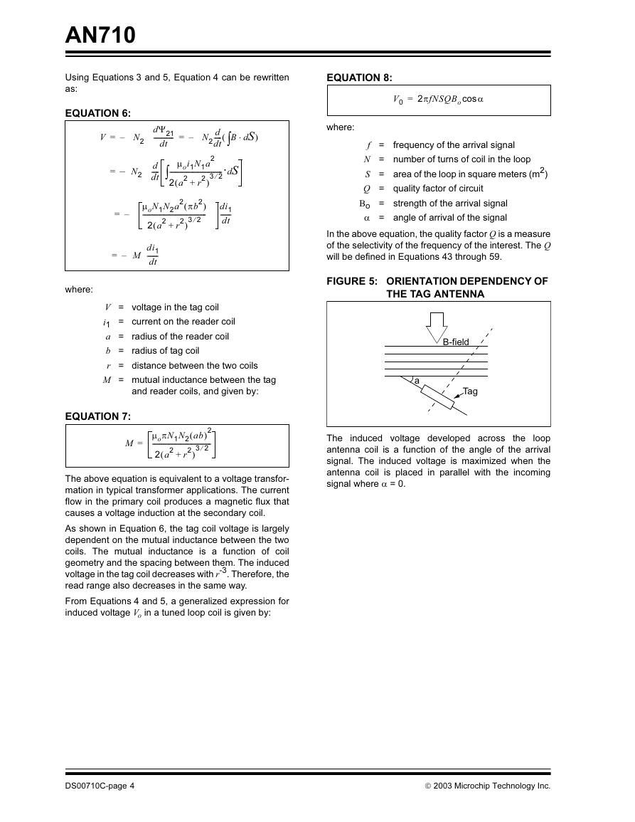
FIGURE 5: Orientation Dependency of the Tag Antenna
Wire Types and Ohmic Losses
DC Resistance of Conductor and Wire Types
AC Resistance of Conductor
Resistance of Conductor with Low Frequency Approximation
TABLE 5: AWG Wire Chart
Inductance of Various Antenna Coils
Calculation of Inductance
FIGURE 6: A circular coil with single turn
FIGURE 7: A circular coil with single turn
FIGURE 8: N-turn multilayer circular coil
FIGURE 9: A spiral coil
FIGURE 10: N-turn square loop coil with multilayer
FIGURE 11: N-turn square loop coil with multilayer
FIGURE 12: A straight thin film inductor
FIGURE 13: Square loop inductor with a rectangular cross section
FIGURE 14: One turn Reader antenna
Example with dimension:
FIGURE 15: Two conductor segments for mutual inductance calculation
Configuration of Antenna Circuits
Reader Antenna Circuits
FIGURE 16: Various Reader Antenna Circuits
Tag Antenna Circuits
Consideration on Quality Factor Q and Bandwidth of Tuning Circuit
FIGURE 17: Various External Circuit Configurations
Bandwidth requirement and limit on circuit Q for MCRF355
Resonant Circuits
Parallel Resonant Circuit
FIGURE 18: Parallel Resonant Circuit
Series Resonant Circuit
FIGURE 19: Series Resonance Circuit
Tuning Method
FIGURE 20: Voltage vs. Frequency for Resonant Circuit
FIGURE 21: Frequency Responses for Resonant Circuit
Read Range of RFID Devices
FIGURE 22: Read Range vs. Tag Size for Typical Proximity Applications*
FIGURE 23: Read Range vs. Tag Size for Typical Long Range Applications*
Appendix A: Calculation of Mutual Inductance Terms in Equations 36 and 37
Appendix B: Mathlab program example for Example 8
References
Trademarks
Worldwide Sales
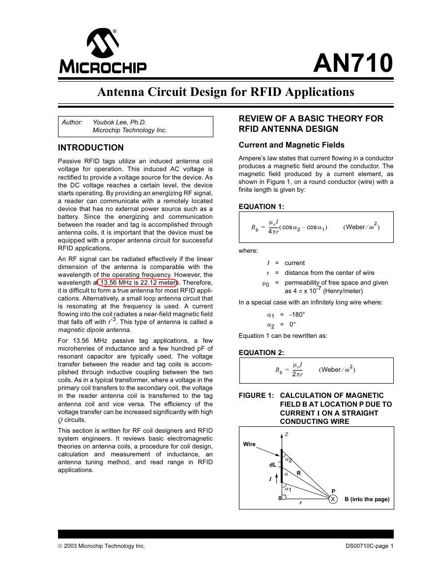
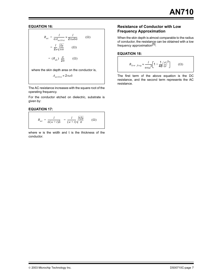
AN710 Antenna Circuit Design for RFID Applications Author: Youbok Lee, Ph.D. Microchip Technology Inc. REVIEW OF A BASIC THEORY FOR RFID ANTENNA DESIGN INTRODUCTION Current and Magnetic Fields Passive RFID tags utilize an induced antenna coil voltage for operation. This induced AC voltage is rectified to provide a voltage source for the device. As the DC voltage reaches a certain level, the device starts operating. By providing an energizing RF signal, a reader can communicate with a remotely located device that has no external power source such as a battery. Since the energizing and communication between the reader and tag is accomplished through antenna coils, it is important that the device must be equipped with a proper antenna circuit for successful RFID applications. An RF signal can be radiated effectively if the linear dimension of the antenna is comparable with the wavelength of the operating frequency. However, the wavelength at 13.56 MHz is 22.12 meters. Therefore, it is difficult to form a true antenna for most RFID appli- cations. Alternatively, a small loop antenna circuit that is resonating at the frequency is used. A current flowing into the coil radiates a near-field magnetic field that falls off with r-3. This type of antenna is called a magnetic dipole antenna. For 13.56 MHz passive tag applications, a few microhenries of inductance and a few hundred pF of resonant capacitor are typically used. The voltage transfer between the reader and tag coils is accom- plished through inductive coupling between the two coils. As in a typical transformer, where a voltage in the primary coil transfers to the secondary coil, the voltage in the reader antenna coil is transferred to the tag antenna coil and vice versa. The efficiency of the voltage transfer can be increased significantly with high Q circuits. This section is written for RF coil designers and RFID system engineers. It reviews basic electromagnetic theories on antenna coils, a procedure for coil design, calculation and measurement of inductance, an antenna tuning method, and read range in RFID applications. Ampere’s law states that current flowing in a conductor produces a magnetic field around the conductor. The magnetic field produced by a current element, as shown in Figure 1, on a round conductor (wire) with a finite length is given by: EQUATION 1: = Bφ µ oI --------- 4πr ( cos α 2 – cos α ) 1 ( Weber m ⁄ 2 ) where: I = current r = distance from the center of wire µ 0 = permeability of free space and given as 4 π x 10-7 (Henry/meter) In a special case with an infinitely long wire where: α α 1 = -180° 2 = 0° Equation 1 can be rewritten as: EQUATION 2: = Bφ µ oI --------- 2πr ( Weber m ⁄ 2 ) FIGURE 1: CALCULATION OF MAGNETIC FIELD B AT LOCATION P DUE TO CURRENT I ON A STRAIGHT CONDUCTING WIRE Wire Ζ α 2 α R α 1 0 r dL I P X B (into the page)  2003 Microchip Technology Inc. DS00710C-page 1
AN710 The magnetic field produced by a circular loop antenna is given by: EQUATION 3: FIGURE 2: CALCULATION OF MAGNETIC FIELD B AT LOCATION P DUE TO CURRENT I ON THE LOOP = Bz = µ 2 ---------------------------------- )3 2⁄ oINa 2 2+ r 2 a ( 2 µ ------------------ oINa 2   1 -----  3 r for 2 r >>a 2 where I = current a = r = radius of loop distance from the center of loop µ 0 = permeability of free space and given as 4 π x 10-7 (Henry/meter) The above equation indicates that the magnetic field strength decays with 1/r3. A graphical demonstration is shown in Figure 3. It has maximum amplitude in the plane of the loop and directly proportional to both the current and the number of turns, N. Equation 3 is often used to calculate the ampere-turn requirement for read range. A few examples that calculate the ampere-turns and the field intensity necessary to power the tag will be given in the following sections. X α a coil I y = V Vo sin ωt R r P Bz z FIGURE 3: DECAYING OF THE MAGNETIC FIELD B VS. DISTANCE r B r-3 r DS00710C-page 2  2003 Microchip Technology Inc.
AN710 INDUCED VOLTAGE IN AN ANTENNA EQUATION 5: COIL Faraday’s law states that a time-varying magnetic field through a surface bounded by a closed path induces a voltage around the loop. Figure 4 shows a simple geometry of an RFID applica- tion. When the tag and reader antennas are in close proximity, the time-varying magnetic field B that is produced by a reader antenna coil induces a voltage (called electromotive force or simply EMF) in the closed tag antenna coil. The induced voltage in the coil causes a flow of current on the coil. This is called Faraday’s law. The induced voltage on the tag antenna coil is equal to the time rate of change of the magnetic flux Ψ. EQUATION 4: V –= N dψ ------- dt where: N = number of turns in the antenna coil Ψ = magnetic flux through each turn The negative sign shows that the induced voltage acts in such a way as to oppose the magnetic flux producing it. This is known as Lenz’s law and it emphasizes the fact that the direction of current flow in the circuit is such that the induced magnetic field produced by the induced current will oppose the original magnetic field. The magnetic flux Ψ in Equation 4 is the total magnetic field B that is passing through the entire surface of the antenna coil, and found by: ψ ∫= B · Sd where: B = magnetic field given in Equation 2 S = surface area of the coil • = inner product (cosine angle between two vectors) of vectors B and surface area S Note: Both magnetic field B and surface S are vector quantities. The presentation of inner product of two vectors in Equation 5 suggests that the total magnetic flux ψ that is passing through the antenna coil is affected by an orientation of the antenna coils. The inner product of two vectors becomes minimized when the cosine angle between the two are 90 degrees, or the two (B field and the surface of coil) are perpendicular to each other and maximized when the cosine angle is 0 degrees. The maximum magnetic flux that is passing through the tag coil is obtained when the two coils (reader coil and tag coil) are placed in parallel with respect to each other. This condition results in maximum induced volt- age in the tag coil and also maximum read range. The inner product expression in Equation 5 also can be expressed in terms of a mutual coupling between the reader and tag coils. The mutual coupling between the two coils is maximized in the above condition. FIGURE 4: A BASIC CONFIGURATION OF READER AND TAG ANTENNAS IN RFID APPLICATIONS Tag Coil V = V0sin(ωt) Tag B = B0sin(ωt) I = I0sin(ωt) Reader Electronics Tuning Circuit Reader Coil  2003 Microchip Technology Inc. DS00710C-page 3
AN710 Using Equations 3 and 5, Equation 4 can be rewritten as: EQUATION 8: = V0 2πfNSQBo αcos EQUATION 6: = – V N2 dΨ 21 ------------- dt = – N2 ( d ----- B∫ dt Sd⋅ ) where: –= N2 d ----- dt ∫ 2 µ oi1N1a 2 2+ r ---------------------------------- · Sd 2 a )3 2⁄ ( f = frequency of the arrival signal N = number of turns of coil in the loop S = area of the loop in square meters (m2) Q = quality factor of circuit Β o = strength of the arrival signal α = angle of arrival of the signal In the above equation, the quality factor Q is a measure of the selectivity of the frequency of the interest. The Q will be defined in Equations 43 through 59. FIGURE 5: ORIENTATION DEPENDENCY OF THE TAG ANTENNA B-field a Tag The induced voltage developed across the loop antenna coil is a function of the angle of the arrival signal. The induced voltage is maximized when the antenna coil is placed in parallel with the incoming signal where α = 0. –= 2 ) µ ----------------------------------------- oN1N2a ( 2+ r 2 πb ( )3 2⁄ 2 a 2 di1 ------- dt –= M di1 ------- dt where: V = voltage in the tag coil i1 = current on the reader coil a = radius of the reader coil b = radius of tag coil r = distance between the two coils M = mutual inductance between the tag and reader coils, and given by: EQUATION 7: M = )2 µ πN1N2 ab( o -------------------------------------- )3 2⁄ ( 2+ r 2 a 2 The above equation is equivalent to a voltage transfor- mation in typical transformer applications. The current flow in the primary coil produces a magnetic flux that causes a voltage induction at the secondary coil. As shown in Equation 6, the tag coil voltage is largely dependent on the mutual inductance between the two coils. The mutual inductance is a function of coil geometry and the spacing between them. The induced voltage in the tag coil decreases with r-3. Therefore, the read range also decreases in the same way. From Equations 4 and 5, a generalized expression for induced voltage Vo in a tuned loop coil is given by: DS00710C-page 4  2003 Microchip Technology Inc.
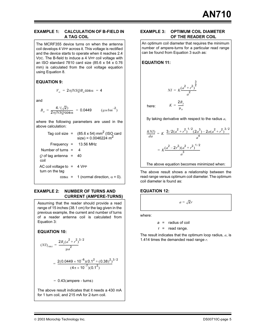
EXAMPLE 1: CALCULATION OF B-FIELD IN EXAMPLE 3: OPTIMUM COIL DIAMETER A TAG COIL OF THE READER COIL AN710 The MCRF355 device turns on when the antenna coil develops 4 VPP across it. This voltage is rectified and the device starts to operate when it reaches 2.4 VDC. The B-field to induce a 4 VPP coil voltage with an ISO standard 7810 card size (85.6 x 54 x 0.76 mm) is calculated from the coil voltage equation using Equation 8. EQUATION 9: An optimum coil diameter that requires the minimum number of ampere-turns for a particular read range can be found from Equation 3 such as: EQUATION 11: = Vo 2πfNSQBo cos α 4= NI = K --- 2 3 2 ) ( a ------------------------- 2+ r 2 a and = Bo ⁄ 4 ) 2( ----------------------------------- 2πfNSQ αcos = 0.0449 ( µwbm 2– ) where: = K 2Bz --------- µ o where the following parameters are used in the above calculation: Tag coil size = (85.6 x 54) mm2 (ISO card size) = 0.0046224 m2 Frequency = 13.56 MHz Number of turns = 4 Q of tag antenna coil = 40 AC coil voltage to turn on the tag = 4 VPP cosα = 1 (normal direction, α = 0). By taking derivative with respect to the radius a, ) ( d NI -------------- da = K )3 2⁄ 3 2⁄ ---------------------------------------------------------------------------------------------------- ) 2a a ( – )1 2⁄ 2+ r 2+ r a ( ( 2 3 2 2a 4 a = K 2 )1 2⁄ ( a -------------------------------------------------------- 2+ r 2r – 2 2 ) a ( 3 a The above equation becomes minimized when: The above result shows a relationship between the read range versus optimum coil diameter. The optimum coil diameter is found as: EXAMPLE 2: NUMBER OF TURNS AND EQUATION 12: CURRENT (AMPERE-TURNS) Assuming that the reader should provide a read range of 15 inches (38.1 cm) for the tag given in the previous example, the current and number of turns of a reader antenna coil is calculated from Equation 3: EQUATION 10: a 2= r where: a = radius of coil r = read range. 3 2⁄ The result indicates that the optimum loop radius, a, is 1.414 times the demanded read range r. 2 ) ( 2+ 2Bz a r ------------------------------- µa 2 ( 6– ) )2 2 0.0449 10 --------------------------------------------------------------------------------------- × ) 0.1 ( + ) 0.1 ( 7– × 4π 10 0.38 ( ) ( 2 2 3 2⁄ 0.43 ampere - turns ( ) ( ) NI rms = = = The above result indicates that it needs a 430 mA for 1 turn coil, and 215 mA for 2-turn coil.  2003 Microchip Technology Inc. DS00710C-page 5
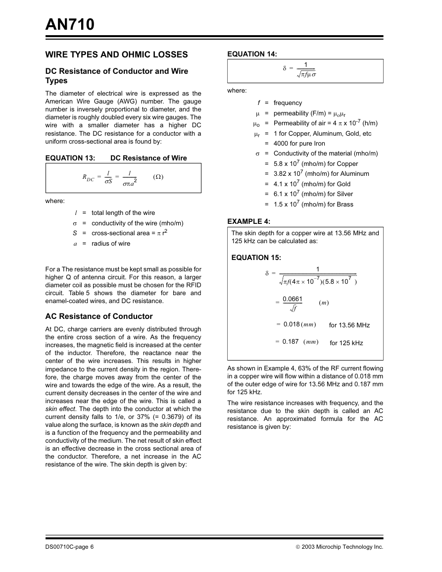
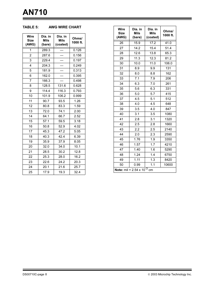
AN710 WIRE TYPES AND OHMIC LOSSES EQUATION 14: DC Resistance of Conductor and Wire Types The diameter of electrical wire is expressed as the American Wire Gauge (AWG) number. The gauge number is inversely proportional to diameter, and the diameter is roughly doubled every six wire gauges. The wire with a smaller diameter has a higher DC resistance. The DC resistance for a conductor with a uniform cross-sectional area is found by: EQUATION 13: DC Resistance of Wire RDC = l ------ σS = l ------------- σπa 2 Ω( ) where: l = total length of the wire σ = conductivity of the wire (mho/m) S = cross-sectional area = π r2 a = radius of wire For a The resistance must be kept small as possible for higher Q of antenna circuit. For this reason, a larger diameter coil as possible must be chosen for the RFID circuit. Table 5 shows the diameter for bare and enamel-coated wires, and DC resistance. AC Resistance of Conductor At DC, charge carriers are evenly distributed through the entire cross section of a wire. As the frequency increases, the magnetic field is increased at the center of the inductor. Therefore, the reactance near the center of the wire increases. This results in higher impedance to the current density in the region. There- fore, the charge moves away from the center of the wire and towards the edge of the wire. As a result, the current density decreases in the center of the wire and increases near the edge of the wire. This is called a skin effect. The depth into the conductor at which the current density falls to 1/e, or 37% (= 0.3679) of its value along the surface, is known as the skin depth and is a function of the frequency and the permeability and conductivity of the medium. The net result of skin effect is an effective decrease in the cross sectional area of the conductor. Therefore, a net increase in the AC resistance of the wire. The skin depth is given by: δ = 1 ----------------- πfµσ where: f = frequency µ = permeability (F/m) = µ µo = Permeability of air = 4 π x 10-7 (h/m) µr = 1 for Copper, Aluminum, Gold, etc µr ο = 4000 for pure Iron σ = Conductivity of the material (mho/m) = 5.8 x 10⁷ (mho/m) for Copper = 3.82 x 10⁷ (mho/m) for Aluminum = 4.1 x 10⁷ (mho/m) for Gold = 6.1 x 10⁷ (mho/m) for Silver = 1.5 x 10⁷ (mho/m) for Brass EXAMPLE 4: The skin depth for a copper wire at 13.56 MHz and 125 kHz can be calculated as: EQUATION 15: δ = ------------------------------------------------------------------------ ) πf 4π 10 ) 5.8 10 ( × ( 1 7– × 7 0.0661 ------------------ = f m( ) = 0.018 mm( ) for 13.56 MHz = 0.187 mm( ) for 125 kHz As shown in Example 4, 63% of the RF current flowing in a copper wire will flow within a distance of 0.018 mm of the outer edge of wire for 13.56 MHz and 0.187 mm for 125 kHz. The wire resistance increases with frequency, and the resistance due to the skin depth is called an AC resistance. An approximated formula for the AC resistance is given by: DS00710C-page 6  2003 Microchip Technology Inc.
AN710 Resistance of Conductor with Low Frequency Approximation When the skin depth is almost comparable to the radius of conductor, the resistance can be obtained with a low frequency approximation[5]: EQUATION 18: Rlow freq ≈ l ------------- 1 σπa 2 +   2 1 ------ a δ---  48 Ω( ) The first term of the above equation is the DC resistance, and the second term represents the AC resistance. EQUATION 16: = Rac = l -------------------- σAactive fµ l πσ------- ------ 2a = ( Rdc ) a 2δ------ ≈ l ----------------- 2πaδσ Ω( ) Ω( ) Ω( ) where the skin depth area on the conductor is, Aactive 2πaδ ≈ The AC resistance increases with the square root of the operating frequency. For the conductor etched on dielectric, substrate is given by: EQUATION 17: = Rac l ------------------------ σ w t+( )δ = l ---------------- w t+( ) πfµ σ--------- Ω( ) where w is the width and t is the thickness of the conductor.  2003 Microchip Technology Inc. DS00710C-page 7
AN710 TABLE 5: AWG WIRE CHART Wire Size (AWG) Dia. in Dia. in Mils (bare) Mils (coated) Ohms/ 1000 ft. 1 2 3 4 5 6 7 8 9 10 11 12 13 14 15 16 17 18 19 20 21 22 23 24 25 289.3 287.6 229.4 204.3 181.9 162.0 166.3 128.5 114.4 101.9 90.7 80.8 72.0 64.1 57.1 50.8 45.3 40.3 35.9 32.0 28.5 25.3 22.6 20.1 17.9 — — — — — — — 131.6 116.3 106.2 93.5 83.3 74.1 66.7 59.5 52.9 47.2 42.4 37.9 34.0 30.2 28.0 24.2 21.6 19.3 0.126 0.156 0.197 0.249 0.313 0.395 0.498 0.628 0.793 0.999 1.26 1.59 2.00 2.52 3.18 4.02 5.05 6.39 8.05 10.1 12.8 16.2 20.3 25.7 32.4 Wire Size (AWG) Dia. in Dia. in Mils (bare) Mils (coated) Ohms/ 1000 ft. 26 27 28 29 30 31 32 33 34 35 36 37 38 39 40 41 42 43 44 45 46 47 48 49 15.9 14.2 12.6 11.3 10.0 8.9 8.0 7.1 6.3 5.6 5.0 4.5 4.0 3.5 3.1 2.8 2.5 2.2 2.0 1.76 1.57 1.40 1.24 1.11 17.2 15.4 13.8 12.3 11.0 9.9 8.8 7.9 7.0 6.3 5.7 5.1 4.5 4.0 3.5 3.1 2.8 2.5 2.3 1.9 1.7 1.6 1.4 1.3 50 1.1 Note: mil = 2.54 x 10⁻³ cm 0.99 41.0 51.4 65.3 81.2 106.0 131 162 206 261 331 415 512 648 847 1080 1320 1660 2140 2590 3350 4210 5290 6750 8420 10600 DS00710C-page 8  2003 Microchip Technology Inc.
分享到:
收藏