SERIAL INTERFACE FOR DATA CONVERTERS
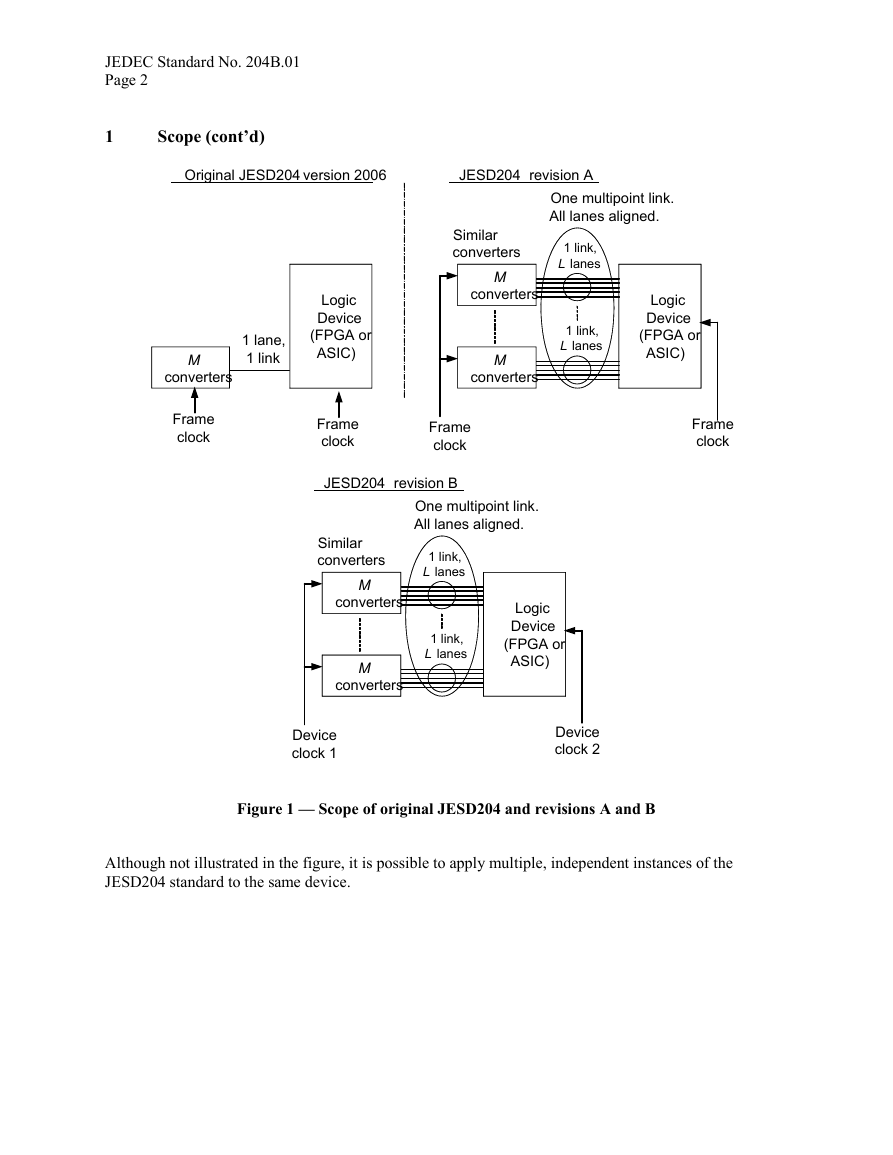
1 Scope
2 References
2.1 Normative
2.2 Informative
3 Terminology
3.1 Terms and definitions
3.1 Terms and definitions (cont’d)
3.1 Terms and definitions (cont’d)
3.1 Terms and definitions (cont’d)
3.2 Meaning of symbols and abbreviations
3.2 Meaning of symbols and abbreviations (cont’d)
Table 1 — Special symbols and operators
4 Electrical specification
4.1 Electrical specification overview
4.1 Electrical specification overview (cont’d)
4.2 Compliance types
4.3 Interconnect
4.3.1 Interconnect Insertion Loss
4.3.1 Interconnect Insertion Loss (cont’d)
4.4 LV-OIF-SxI5 Data interface signals (Differential)
4.4.1 Compliance verification
4.4.2 LV-OIF-SxI5 Transmitter Electrical Specifications
Table 2 — General differential output DC and AC characteristics for LV-OIF-SxI5 – based operation
4.4.2 LV-OIF-SxI5 Transmitter Electrical Specifications (cont’d)
4.4.3 LV-OIF-SxI5 Receiver Electrical Specifications
4.4.3 LV-OIF-SxI5 Receiver Electrical Specifications (cont’d)
4.5 LV-OIF-6G-SR Data interface signals (Differential)
4.5.1 Compliance verification
4.5.2 LV-OIF-6G-SR Transmitter Electrical specifications
Table 4 — General differential output DC and AC characteristics for LV-OIF-6G-SR – based operation
4.5.2 LV-OIF-6G-SR Transmitter Electrical specifications (cont’d)
4.5.3 LV-OIF-6G-SR Receiver specifications
Table 5 — General Differential Input DC and AC Characteristics for LV-OIF-6G-SR – based operation
4.5.3 LV-OIF-6G-SR Receiver specifications (cont’d)
4.6 LV-OIF-11G-SR Data interface signals (Differential)
4.6.1 Compliance verification
4.6.2 LV-OIF-11G-SR Transmitter Electrical specifications
Table 6 — General differential output DC and AC characteristics for LV-OIF-11G-SR – based operation
4.6.2 LV-OIF-11G-SR Transmitter Electrical specifications (cont’d)
4.6.3 LV-OIF-11G-SR Receiver specifications
Table 7 — General Differential Input DC and AC Characteristics for LV-OIF-11G-SR – based operation
4.6.3 LV-OIF-11G-SR Receiver specifications (cont’d)
4.7 Device clock
4.8 Frame Clock, and Local Multiframe Clock
4.8 Frame Clock, and Local Multiframe Clock (cont’d)
4.9 SYNC interface
4.9 SYNC interface (cont’d)
4.9 SYNC interface (cont’d)
4.10 Lane-to-lane inter-device synchronization interface
4.11 SYSREF signal (Device Subclass 1)
4.11 SYSREF signal (Device Subclass 1) (cont’d)
4.12 Skew and misalignment budget
4.12 Skew and misalignment budget (cont’d)
4.12 Skew and misalignment budget (cont’d)
4.12 Skew and misalignment budget (cont’d)
4.12 Skew and misalignment budget (cont’d)
4.12 Skew and misalignment budget (cont’d)
4.12 Skew and misalignment budget (cont’d)
4.12 Skew and misalignment budget (cont’d)
4.13 Control Interfaces (informative)
5 Data stream
5.1 Transport layer
5.1.1 Overview
5.1.2 User data format for an independent lane
5.1.2.1 User data mapping without oversampling
5.1.2.1 User data mapping without oversampling (cont’d)
5.1.2.1 User data mapping without oversampling (cont’d)
5.1.3 User data format for multiple lanes
5.1.3 User data format for multiple lanes
5.1.3 User data format for multiple lanes (cont’d)
5.1.4 Tail bits
5.1.5 Idle mode
5.1.5.1 General
5.1.5.2 Dummy samples
5.1.6 Test modes (transport layer)
5.1.6.1 General
5.1.6.2 Short transport layer test pattern
5.1.6.3 Long transport layer test pattern
5.2 Scrambling
5.2.1 Scrambler polynomial
5.2.2 Scrambler bit order
5.2.3 Scrambler type
5.2.3 Scrambler type (cont’d)
5.2.4 Early synchronization option
/
5.2.5 Initial state
5.2.6 Scrambling disable
5.3 Data Link Layer
5.3.1 8B/10B encoding
5.3.2 Transmission order
5.3.3 Link operation
5.3.3.1 Code group synchronization
5.3.3.1 Code group synchronization (cont’d)
5.3.3.2 SYNC~ signal combining
5.3.3.2 SYNC~ signal combining (cont’d)
5.3.3.3 Initial frame synchronization
5.3.3.4 Frame alignment monitoring and correction
5.3.3.4.1 Alignment characters
5.3.3.4.2 Character replacement without scrambling
5.3.3.4.3 Character replacement with scrambling
5.3.3.4.4 Frame alignment correction in the RX
5.3.3.5 Initial lane synchronization
5.3.3.5 Initial lane synchronization (cont’d)
5.3.3.6 Lane alignment monitoring and correction
5.3.3.7 Link re-initialization
5.3.3.7 Link re-initialization (cont’d)
5.3.3.8 Test modes
5.3.3.8.1 General
5.3.3.8.2 Test sequences
5.3.3.8.2 Test sequences (cont’d)
6.1 Introduction
6.1 Introduction (cont’d)
6.2 No Support for Determisitic Latency (Device Subclass 0) (Informative)
6.3 Deterministic Latency Using SYSREF (Device Subclass 1)
6.3 Deterministic Latency Using SYSREF (Device Subclass 1) (cont’d)
6.3 Deterministic Latency Using SYSREF (Device Subclass 1) (cont’d)
6.3 Deterministic Latency Using SYSREF (Device Subclass 1) (cont’d)
6.4 Deterministic Latency Using SYNC~ Detection (Device Subclass 2)
6.4 Deterministic Latency Using SYNC~ Detection (Device Subclass 2)
6.4.1 Principles of SYNC~ sampling
6.4.1.1 SYNC~ generation at the RX device
6.4.1.2 Adjustment resolution and adjustment clock
6.4.1.2 Adjustment resolution and adjustment clock (cont’d)
6.4.1.3 Detection resolution at the TX device
6.4.1.4 SYNC~ de-assertion detection and the detection interval
6.4.1.4 SYNC~ de-assertion detection and the detection interval (cont’d)
6.4.2 Master and slave configurations
6.4.2.1 ADC Master and slave configuration
6.4.2.1 ADC Master and slave configuration (cont’d)
6.4.2.2 DAC master and slave configurations
6.4.2.2 DAC master and slave configurations (cont’d)
6.4.2.2 DAC master and slave configurations (cont’d)
6.4.2.2 DAC master and slave configurations (cont’d)
Loop initialization
Latency monitoring:
6.4.3 Summary of requirements for subclass 2 deterministic latency
General requirements for support of subclass 2 protocol.
Requirement for subclass 2 TX converter devices.
Requirement for subclass 2 RX converter devices.
Requirement for a TX logic device for subclass 2 support.
6.5 Interoperability Between JESD204A and JESD204B Devices
7 Receiver Operation
7.1 Code group synchronization
7.1 Code group synchronization (cont’d)
7.2 Initial frame synchronization
7.2 Initial frame synchronization (cont’d)
7.3 Frame alignment monitoring and correction
7.3 Frame alignment monitoring and correction (cont’d)
7.4 Initial lane synchronization
7.5 Lane alignment monitoring and correction
7.5 Lane alignment monitoring and correction (cont’d)
7.6 Error handling
7.6.1 Error kinds
7.6.2 Data output on error
7.6.4 Error reporting via SYNC interface
7.6.5 Error reporting via control interface
8.1 Synchronization
8.1 Synchronization (cont’d)
8.2 Initial lane alignment sequence
8.3 Link configuration data and encoding
8.3 Link configuration data and encoding
8.3 Link configuration data and encoding (cont’d)
8.4 SYNC signal decoding
8.4 SYNC signal decoding (cont’d)
8.5 SYNC~ detection (device subclass 2)
9 Device classification
9.1 Device Subclassification
Annex A (informative) Differences between JESD204B.01 and JESD204B
3.2 Meaning of symbols and abbreviations
Annex A (informative) Differences between JESD204B and JESD204A (cont’d)
4.2 Compliance types
4.3 Interconnect
4.3.1 Interconnect Insertion Loss
4.4 LV-OIF-SxI5 Data interface signals (Differential)
4.4.1 Compliance verification
4.4.2 LV-OIF-SxI5 Transmitter Electrical Specifications
4.4.3 LV-OIF-SxI5 Receiver Electrical Specifications
4.5 LV-OIF-6G-SR Data interface signals (Differential)
4.6 LV-OIF-11G-SR Data interface signals (Differential)
4.7 Device clock
4.8 Frame Clock, and Local Multiframe Clock.
4.9 SYNC interface
Annex A (informative) Differences between JESD204B and JESD204A (cont’d)
4.10 Lane-to-lane inter-device synchronization interface
4.11 SYSREF signal (Device Subclass 1)
4.12 Skew and misalignment budget
4.13 Control Interfaces (informative)
5.1.2 User data format for an independent lane
5.1.3 User data format for multiple lanes
5.1.6 Test modes (transport layer)
5.1.6.1 General
5.1.6.2 Short transport layer test pattern
5.1.6.3 Long transport layer test pattern
5.2 Scrambling
Annex A (informative) Differences between JESD204B and JESD204A (cont’d)
5.2.6 Scrambling disable
5.3.3.1 Code group synchronization
5.3.3.4.2 Character replacement without scrambling
5.3.3.4.3 Character replacement with scrambling
5.3.3.4.4 Frame alignment correction in the RX
5.3.3.5 Initial lane synchronization
5.3.3.6 Lane alignment monitoring and correction
5.3.3.7 Link re-initialization
5.3.3.8 Test modes
5.3.3.8.2 Test sequences
6 Deterministic Latency
7 Receiver Operation
Annex A (informative) Differences between JESD204B and JESD204A (cont’d)
7.1 Code group synchronization
7.4 Initial lane synchronization
7.5 Lane alignment monitoring and correction
7.6.4 Error reporting via SYNC interface
8 Transmitter Operation
8.1 Synchronization
8.2 Initial lane alignment sequence
8.3 Link configuration data and encoding
8.4 SYNC signal decoding
8.5 SYNC~ detection (device subclass 2)
Annex A (informative) Differences between JESD204B and JESD204A (cont’d)
9 Device classification
9.1 Device Subclassification
Annex B (informative) Application overview
Annex C (informative) Device level implementation
Annex E (informative) Instructions for Determining Linear Fitted Insertion Loss
Annex F (informative) Example of device clock and SYSREF generation
Annex G (informative) Clock Terminology
Annex B (informative) Application overview
B.1 Background
B.2 Link properties
B.3 Variants and modes
B.4 Configuration examples
B.4.1 General
B.4.2 Single Device ADC Application
B.4.3 Single Device DAC Application
B.4.4 Multiple Device ADC Application
B.4.5 Multiple Device DAC Application
B.4.6 Interface for Decimating or Oversampled ADC
B.4.7 Interface for Interpolating or Oversampled DAC
Annex C (informative) Device level implementation
C.1 Transmitter block
C.1.1 Generic structure
C.1.2 TX Link Layer
C.1.3 TX Physical Layer
C.2 Receiver block
C.2.1 Generic structure
C.2.2 RX Link Layer
C.2.3 RX Physical Layer
Annex E (informative) Instructions for Determining Linear Fitted Insertion Loss
Annex F (informative) Example of device clock and SYSREF generation
Annex G (informative) Clock Terminology
Standard Improvement Form JEDEC JESD204B.01
Table 21




 2023年江西萍乡中考道德与法治真题及答案.doc
 2012年重庆南川中考生物真题及答案.doc
 2013年江西师范大学地理学综合及文艺理论基础考研真题.doc
 2020年四川甘孜小升初语文真题及答案I卷.doc
 2020年注册岩土工程师专业基础考试真题及答案.doc
 2023-2024学年福建省厦门市九年级上学期数学月考试题及答案.doc
 2021-2022学年辽宁省沈阳市大东区九年级上学期语文期末试题及答案.doc
 2022-2023学年北京东城区初三第一学期物理期末试卷及答案.doc
 2018上半年江西教师资格初中地理学科知识与教学能力真题及答案.doc
 2012年河北国家公务员申论考试真题及答案-省级.doc
 2020-2021学年江苏省扬州市江都区邵樊片九年级上学期数学第一次质量检测试题及答案.doc
 2022下半年黑龙江教师资格证中学综合素质真题及答案.doc