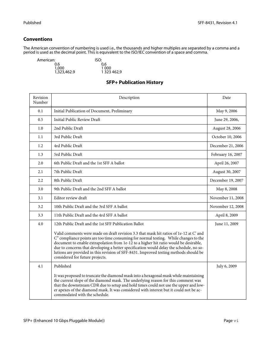
SFP+ Publication History
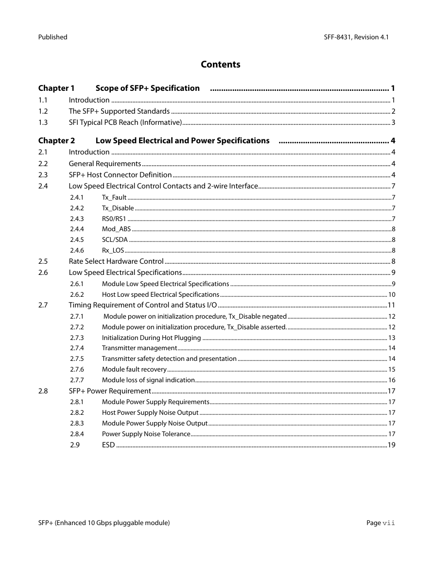
Contents
Chapter 1 Scope of SFP+ Specification 1
Chapter 2 Low Speed Electrical and Power Specifications 4
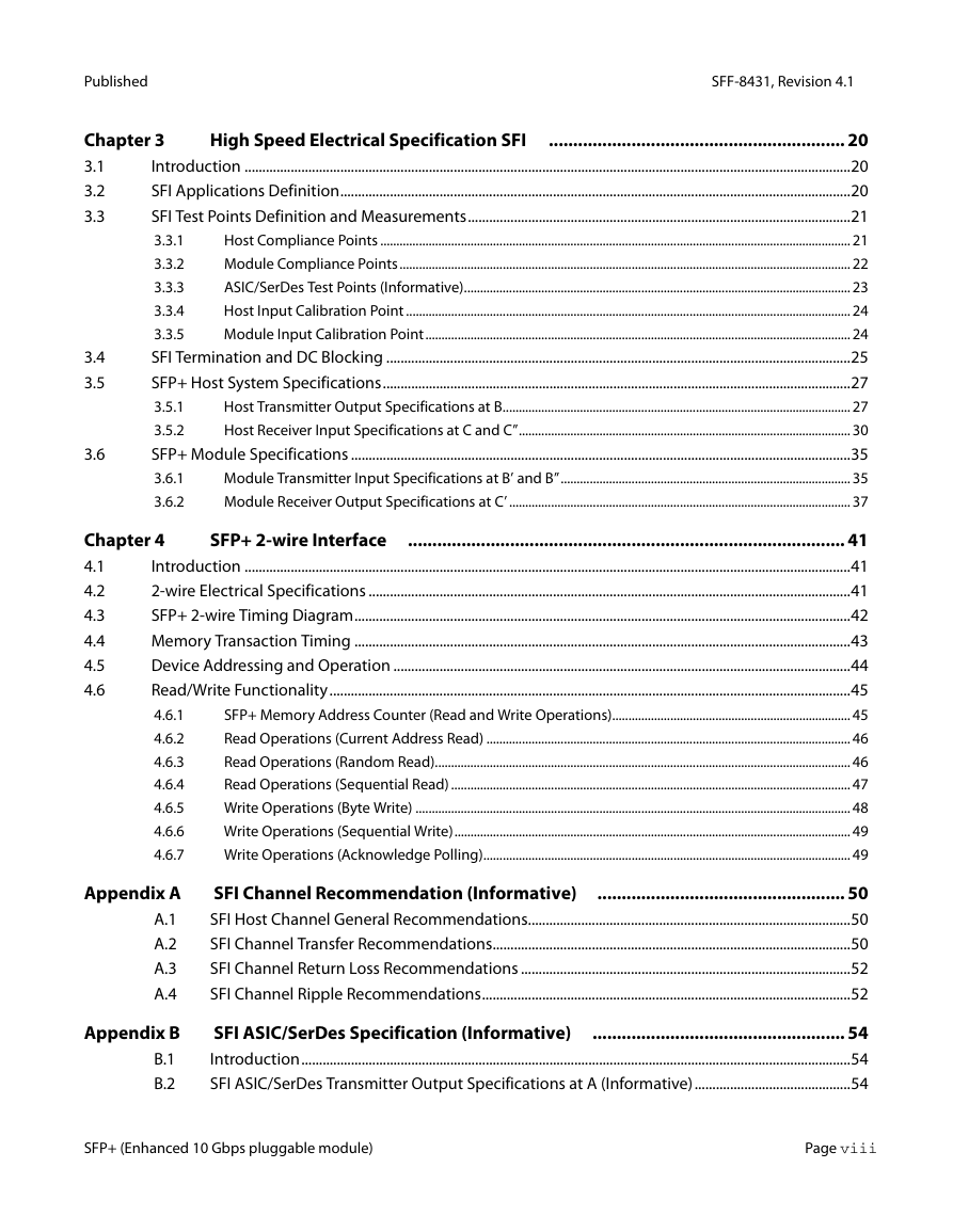
Chapter 3 High Speed Electrical Specification SFI 20
Chapter 4 SFP+ 2-wire Interface 41
List of Tables
List of Figures
Chapter 1 Scope of SFP+ Specification
1.1 Introduction
1.2 The SFP+ Supported Standards
1.3 SFI Typical PCB Reach (Informative)
Chapter 2 Low Speed Electrical and Power Specifications
2.1 Introduction
2.2 General Requirements
2.3 SFP+ Host Connector Definition
2.4 Low Speed Electrical Control Contacts and 2-wire Interface
2.4.1 Tx_Fault
2.4.2 Tx_Disable
2.4.3 RS0/RS1
2.4.4 Mod_ABS
2.4.5 SCL/SDA
2.4.6 Rx_LOS
2.5 Rate Select Hardware Control
2.6 Low Speed Electrical Specifications
2.6.1 Module Low Speed Electrical Specifications
2.6.2 Host Low speed Electrical Specifications
2.7 Timing Requirement of Control and Status I/O
2.7.1 Module power on initialization procedure, Tx_Disable negated
2.7.2 Module power on initialization procedure, Tx_Disable asserted.
2.7.3 Initialization During Hot Plugging
2.7.4 Transmitter management
2.7.5 Transmitter safety detection and presentation
2.7.6 Module fault recovery
2.7.7 Module loss of signal indication
2.8 SFP+ Power Requirement
2.8.1 Module Power Supply Requirements
2.8.2 Host Power Supply Noise Output
2.8.3 Module Power Supply Noise Output
2.8.4 Power Supply Noise Tolerance
2.9 ESD
Chapter 3 High Speed Electrical Specification SFI
3.1 Introduction
3.2 SFI Applications Definition
3.3 SFI Test Points Definition and Measurements
3.3.1 Host Compliance Points
3.3.2 Module Compliance Points
3.3.3 ASIC/SerDes Test Points (Informative)
3.3.4 Host Input Calibration Point
3.3.5 Module Input Calibration Point
3.4 SFI Termination and DC Blocking
3.5 SFP+ Host System Specifications
3.5.1 Host Transmitter Output Specifications at B
3.5.2 Host Receiver Input Specifications at C and C”
3.6 SFP+ Module Specifications
3.6.1 Module Transmitter Input Specifications at B’ and B”
3.6.2 Module Receiver Output Specifications at C’
Chapter 4 SFP+ 2-wire Interface
4.1 Introduction
4.2 2-wire Electrical Specifications
4.3 SFP+ 2-wire Timing Diagram
4.4 Memory Transaction Timing
4.5 Device Addressing and Operation
4.6 Read/Write Functionality
4.6.1 SFP+ Memory Address Counter (Read and Write Operations)
4.6.2 Read Operations (Current Address Read)
4.6.3 Read Operations (Random Read)
4.6.4 Read Operations (Sequential Read)
4.6.5 Write Operations (Byte Write)
4.6.6 Write Operations (Sequential Write)
4.6.7 Write Operations (Acknowledge Polling)
Appendix A SFI Channel Recommendation (Informative)
A.1 SFI Host Channel General Recommendations
A.2 SFI Channel Transfer Recommendations
A.3 SFI Channel Return Loss Recommendations
A.4 SFI Channel Ripple Recommendations
Appendix B SFI ASIC/SerDes Specification (Informative)
B.1 Introduction
B.2 SFI ASIC/SerDes Transmitter Output Specifications at A (Informative)
B.3 SFI ASIC/SerDes Receiver Input Specifications at D (Informative)
Appendix C Application Reference Boards (Normative)
C.1 Compliance Boards
C.1.1 Host Compliance Board Transfer Characteristics
C.1.2 Module Compliance Board Transfer Characteristics
C.1.3 ASIC/SerDes Test Board Transfer Characteristics
C.2 Host Compliance Board
C.2.1 Host Compliance Board Material and Layer Stack-up
C.2.2 Host Compliance Board Partlist
C.2.3 HCB Gerber Files
C.2.4 Schematic of Host Compliance Board
C.3 Module Compliance Board
C.3.1 Module Compliance Board Material and Layer Stack-up
C.3.2 Schematic of Module Compliance Board
C.3.3 Module Compliance Board Partlist
C.3.4 MCB Gerber files
C.4 Specifications for Mated Host and Module Compliance Boards
Appendix D Test Methodology and Measurement (Normative)
D.1 Introduction
D.1.1 Test Patterns
D.2 Eye Mask Compliance
D.2.1 Example Calculations for 5x10⁻⁵ Hit Ratio
D.3 Data Dependent Jitter (DDJ) and Pulse Width Shrinkage (DDPWS)
D.3.1 Duty Cycle Distortion (DCD)
D.4 Uncorrelated Jitter (UJ)
D.5 99% Jitter (J2) and Total Jitter (TJ)
D.6 Rise and Fall Times
D.7 Voltage Modulation Amplitude (VMA)
D.8 Relative Noise (RN)
D.9 Waveform Distortion Penalty (WDP)
D.10 Electrical compliance signal at B” for the SFP+ Module transmitter
D.11 Test Method for a host receiver for a limiting module
D.11.1 Test Equipment & Setup
D.11.2 Stressed-Eye Jitter Characteristics
D.11.3 Calibration
D.11.4 Calibration Procedure
D.11.5 Test Procedure
D.12 Limiting Module Receiver Compliance Tests
D.13 Test Method for a Host Receiver with a Linear Module
D.13.1 Test Description and Procedure for Host Receiver for Linear Module
D.13.2 Host Linear Tester calibration
D.14 Linear Module Receiver Compliance Tests
D.14.1 Linear Module receiver noise compliance test
D.14.2 linear Module Receiver Distortion Penalty Compliance Test
D.14.3 Linear Module Receiver Output Differential Peak-Peak Voltage
D.15 AC Common Mode Voltage
D.15.1 Definition of AC Common Mode Voltage
D.15.2 AC Common Mode Generation Test
D.15.3 AC Common Mode Tolerance Test
D.16 Termination Mismatch
D.17 Power Supply Testing methodology
D.17.1 Host Power Supply Noise Output
D.17.2 SFP+ Module Power Supply Noise Output
D.17.3 Module Power Supply Tolerance Testing
Appendix E SFP+ Direct Attach Cable Specifications “10GSFP+Cu” (Optional)
E.1 10GSFP+Cu Direct Attach Construction
E.2 SFP+ Host Output Specifications for Passive Direct Attach Cables
E.2.1 Transmitter Stressor
E.3 SFP+ Host Receiver Supporting 10GSFP+Cu Input Compliance Test Signal Calibrated at C”
E.3.1 Copper Host Receiver Specifications
E.3.2 Copper Host Stress Generator 1 UI Pulse Response
E.4 SFP+ Passive Direct Attach cable Assembly Specifications
E.4.1 SFP+ Direct Attach Cable Test Setup
E.4.2 Cable dWDP Test Procedure
E.4.3 Cable NEXT Measurement Procedure
E.4.4 VMA to Crosstalk Ratio (VCR)
Appendix F 1.25 GBd Operation Support (Optional)
F.1 Introduction
F.2 SFP+ Host Operation Guideline for Supporting Classic SFP
Appendix G Matlab Code for TWDP


 2023年江西萍乡中考道德与法治真题及答案.doc
 2012年重庆南川中考生物真题及答案.doc
 2013年江西师范大学地理学综合及文艺理论基础考研真题.doc
 2020年四川甘孜小升初语文真题及答案I卷.doc
 2020年注册岩土工程师专业基础考试真题及答案.doc
 2023-2024学年福建省厦门市九年级上学期数学月考试题及答案.doc
 2021-2022学年辽宁省沈阳市大东区九年级上学期语文期末试题及答案.doc
 2022-2023学年北京东城区初三第一学期物理期末试卷及答案.doc
 2018上半年江西教师资格初中地理学科知识与教学能力真题及答案.doc
 2012年河北国家公务员申论考试真题及答案-省级.doc
 2020-2021学年江苏省扬州市江都区邵樊片九年级上学期数学第一次质量检测试题及答案.doc
 2022下半年黑龙江教师资格证中学综合素质真题及答案.doc