IT6801FN
Single-port MHL2.1/HDMI1.4 Receiver with 3D Support
ITE confidential for Zhongxinwei use only
ITE TECH. INC.
www.ite.com.tw
T8720F V0.7.1
Jul-2015 Rev:0.96a 1/44
�
IT6801FN
General Description
provided to support up to compressed audio of 192kHz frame rate.
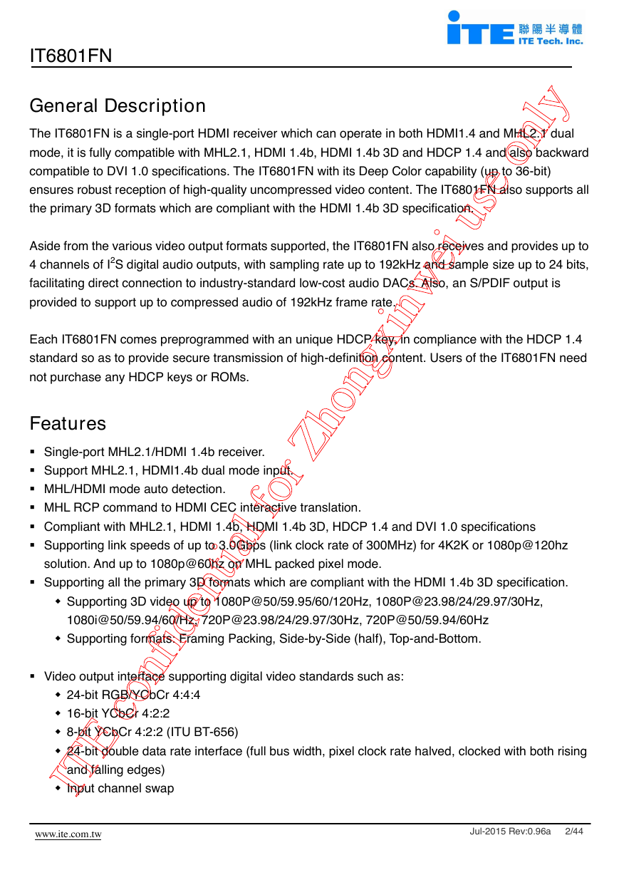
The IT6801FN is a single-port HDMI receiver which can operate in both HDMI1.4 and MHL2.1 dual
mode, it is fully compatible with MHL2.1, HDMI 1.4b, HDMI 1.4b 3D and HDCP 1.4 and also backward
compatible to DVI 1.0 specifications. The IT6801FN with its Deep Color capability (up to 36-bit)
ensures robust reception of high-quality uncompressed video content. The IT6801FN also supports all
the primary 3D formats which are compliant with the HDMI 1.4b 3D specification.
Each IT6801FN comes preprogrammed with an unique HDCP key, in compliance with the HDCP 1.4
standard so as to provide secure transmission of high-definition content. Users of the IT6801FN need
Aside from the various video output formats supported, the IT6801FN also receives and provides up to
4 channels of I2S digital audio outputs, with sampling rate up to 192kHz and sample size up to 24 bits,
facilitating direct connection to industry-standard low-cost audio DACs. Also, an S/PDIF output is
Input channel swap ITE confidential for Zhongxinwei use only
Supporting 3D video up to 1080P@50/59.95/60/120Hz, 1080P@23.98/24/29.97/30Hz,
Supporting formats: Framing Packing, Side-by-Side (half), Top-and-Bottom.
1080i@50/59.94/60/Hz, 720P@23.98/24/29.97/30Hz, 720P@50/59.94/60Hz
solution. And up to 1080p@60hz on MHL packed pixel mode.
8-bit YCbCr 4:2:2 (ITU BT-656)
24-bit RGB/YCbCr 4:4:4
16-bit YCbCr 4:2:2
and falling edges)
Single-port MHL2.1/HDMI 1.4b receiver.
Support MHL2.1, HDMI1.4b dual mode input.
MHL/HDMI mode auto detection.
Compliant with MHL2.1, HDMI 1.4b, HDMI 1.4b 3D, HDCP 1.4 and DVI 1.0 specifications
Supporting link speeds of up to 3.0Gbps (link clock rate of 300MHz) for 4K2K or 1080p@120hz
Supporting all the primary 3D formats which are compliant with the HDMI 1.4b 3D specification.
24-bit double data rate interface (full bus width, pixel clock rate halved, clocked with both rising
Video output interface supporting digital video standards such as:
not purchase any HDCP keys or ROMs.
Features
MHL RCP command to HDMI CEC interactive translation.
www.ite.com.tw
T8720F V0.7.1
Jul-2015 Rev:0.96a 2/44
�
IT6801FN
programmable coefficients.
Auto-calibrated input termination impedance provides process-, voltage- and temperature-invariant
sample sizes of 16~24 bits
S/PDIF interface supporting PCM, Dolby Digital, DTS digital audio at up to 192kHz frame rate
automatic audio error detection for programmable soft mute, preventing annoying harsh output
sound due to audio error or hot-unplug
matching to the input transmission lines.
Integrated programmable EDID RAM
76-pin QFN (9mm x 9mm) package
Digital audio output interface supporting
Integrated pre-programmed HDCP keys
RoHS Compliant ( 100% Green available )
Intelligent, programmable power management
Dithering for conversion from 12-bit component to 8-bit
Up/down sampling between YCbCr 4:4:4 and YCbCr 4:2:2
Bi-direction Color Space Conversion (CSC) between RGB and YCbCr color spaces with
up to two I2S interface supporting 4-channel audio, with sample rates of 32~192 kHz and
ITE confidential for Zhongxinwei use only
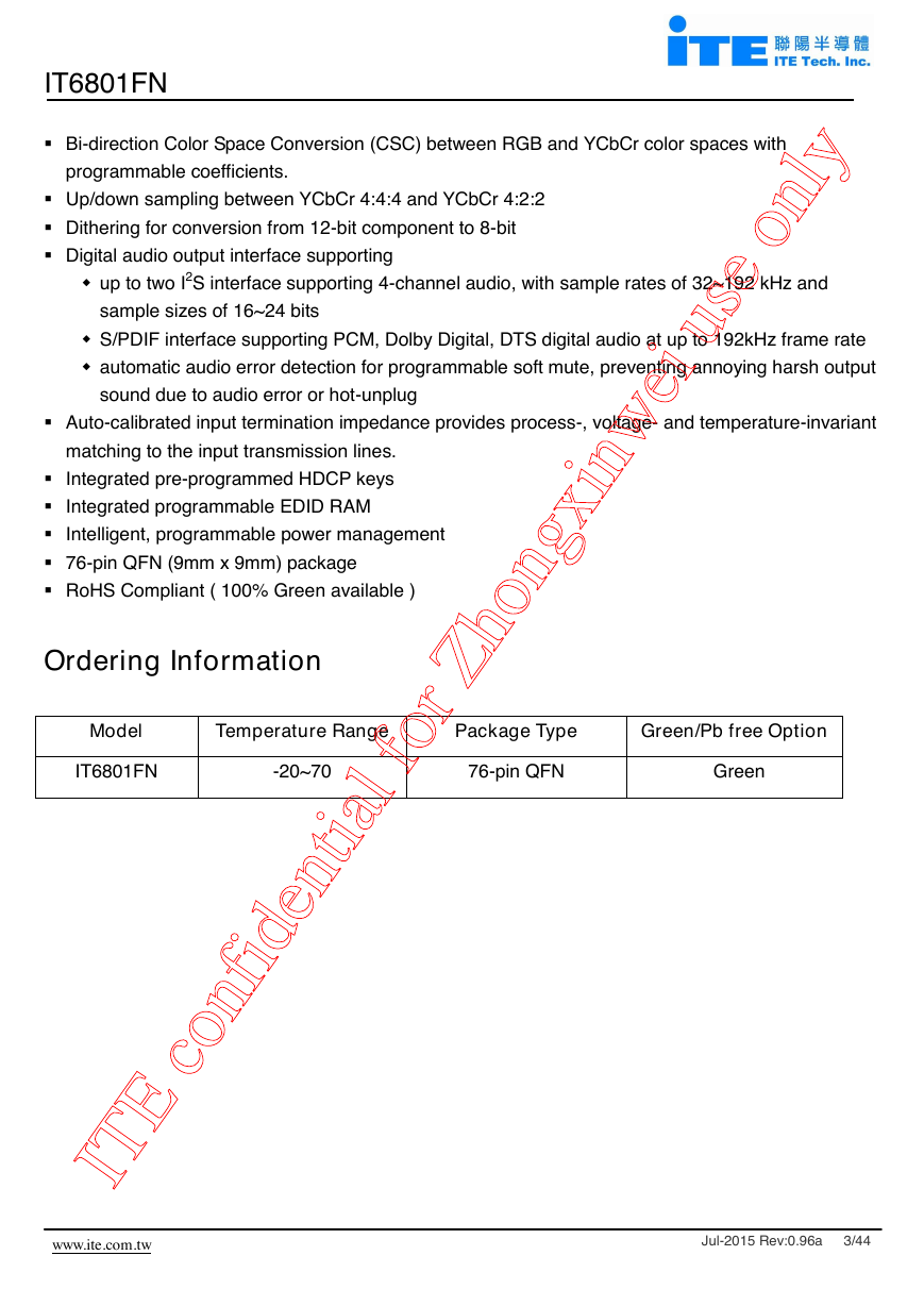
Ordering Information
Model
Temperature Range
Package Type
Green/Pb free Option
IT6801FN
-20~70
76-pin QFN
Green
www.ite.com.tw
T8720F V0.7.1
Jul-2015 Rev:0.96a 3/44
�
IT6801FN
40
41
47
19
18
17
16
15
44
45
46
I2S0
42
14
PCSCL
XTALIN
39
IVDD12
43
38
37
36
35
34
33
32
IVDD12
3
3
C
C
V
P
31
30
29
28
27
26
25
24
23
22
21
20
2
1
C
C
V
P
3
3
C
C
V
A
3
3
C
C
V
A
3
3
C
C
V
A
2
1
C
C
V
A
2
1
D
D
V
D
3
3
D
D
V
O
P
2
X
R
_
0
P
P
0
X
R
_
0
P
P
1
X
R
_
0
P
N
0
X
R
_
0
P
N
2
X
R
_
0
P
N
1
X
R
_
0
P
P
C
X
R
_
0
P
2
1
D
D
V
P
A
APVCC33
T
U
O
L
A
T
X
N
C
X
R
_
0
P
I2S1_3DR
DDCSCL0
SYSRSTN
DDCSDA0
CDSENSE
R0PWR5V
WS_SPDIF
/
D
P
H
S
U
B
C
SCK_MCLK
MUTE_MCLK
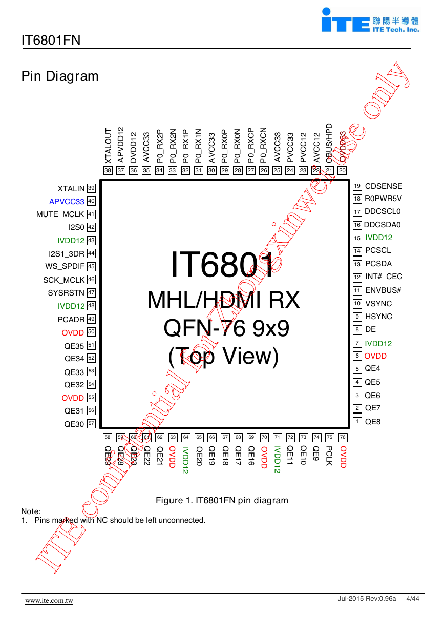
Pin Diagram
IT6801
ITE confidential for Zhongxinwei use only
MHL/HDMI RX
QFN-76 9x9
(Top View)
Note:
1. Pins marked with NC should be left unconnected.
Figure 1. IT6801FN pin diagram
INT#_CEC
9
8
7
6
5
4
3
2
1
IVDD12
48
ENVBUS#
58
59
60
61
62
63
64
65
66
67
68
69
70
71
72
73
74
75
76
I
V
D
D
1
2
I
V
D
D
1
2
QE34
52
IVDD12
HSYNC
PCADR
53
54
55
56
57
13
PCSDA
10
VSYNC
O
V
D
D
O
V
D
D
O
V
D
D
49
50
51
OVDD
OVDD
OVDD
P
C
L
K
Q
E
1
6
Q
E
1
7
QE4
QE5
QE6
QE7
QE8
QE33
QE32
Q
E
2
0
Q
E
1
9
Q
E
1
8
Q
E
2
9
Q
E
2
8
Q
E
2
3
Q
E
2
2
Q
E
2
1
QE31
QE30
QE35
Q
E
1
1
Q
E
1
0
Q
E
9
12
11
DE
www.ite.com.tw
T8720F V0.7.1
Jul-2015 Rev:0.96a 4/44
�
LVTTL
1-5, 51-54, 56-62,
65-69, 72-74
XTALIN
Input
Type
Pin No.
IT6801FN
QE[35:28]
Output
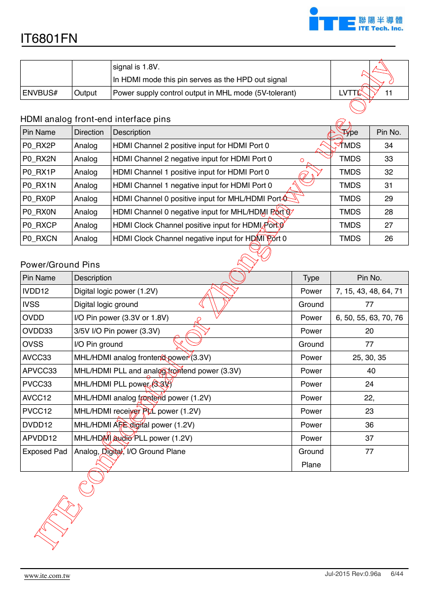
Digital Video Output Pins
Digital Audio Output Pins
DE
HSYNC
VSYNC
Pin Description
Pin Name
XTALOUT
Pin Name
QE[23:16]
QE[11:4]
PCLK
75
Type
LVTTL
Output
Pin No.
LVTTL
LVTTL
LVTTL
8
9
10
Direction Description
Direction Description
Output
Vertical sync. signal
Output
Horizontal sync. signal
Output
Data enable
Crystal clock input (for Audio PLL)
supported through register setting.
Digital Video Output Pins. Channel swap are
Output Crystal clock output (for Audio PLL)
use the rising edge of PCLK to strobe QE Data.
Output data clock. The backend controller should
ITE confidential for Zhongxinwei use only
Interrupt output. Default active-low (5V-tolerant), doubles as CEC
Serial Programming device address select. Device address is
Serial Programming Clock for chip programming (5V-tolerant)
I2S serial clock output, doubles as audio master clock output
Serial Programming Data for chip programming (5V-tolerant)
I2S serial data output, doubles as doubles as 3D R/L signal
In MHL mode this pin is the Control Bus signal. The CBUS
I2S word select output, doubles as S/PDIF audio output
This pin is used to detect MHL connection (5V-tolerant)
TMDS transmitter detection for Port 0(5V-tolerant)
0x90 when PCADR is pulled low, 0x92 otherwise
DDC I2C Clock for HDMI Port 0 (5V-tolerant)
Audio master clock, doubles as Mute output
DDC I2C Data for HDMI Port 0 (5V-tolerant)
Hardware reset pin. Active LOW
Output
I2S serial data output
function I/O (5V-tolerant)
Direction Description
I/O
I/O
Schmitt
Schmitt
Schmitt
LVTTL
LVTTL
LVTTL
LVTTL
Schmitt
LVTTL
LVTTL
LVTTL
Schmitt
Output
Input
I/O
Input
LVTTL
LVTTL
LVTTL
LVTTL
MCLK_MUTE
Output
SCK_MCLK
Output
WS_SPDIF
Output
CDSENSE
Input
CBUS/HPD
I/O
Programming Pins
Pin Name
INT#_CEC
Output
I2S0
I2S1_3DR
SYSRSTN
Input
R0PWR5V
Input
DDCSCL0
DDCSDA0
PCSCL
PCSDA
PCADR
Type
Pin No.
LVTTL
12
39
38
41
46
45
42
44
47
17
16
18
14
13
49
19
21
www.ite.com.tw
T8720F V0.7.1
Jul-2015 Rev:0.96a 5/44
�
IT6801FN
LVTTL
11
Type
Pin No.
34
33
32
31
29
28
27
26
TMDS
Pin Name
signal is 1.8V.
TMDS
TMDS
TMDS
TMDS
ENVBUS#
Output
TMDS
TMDS
TMDS
P0_RX0P
Analog
P0_RX1P
Analog
Pin Name
Description
P0_RX2P
Analog
P0_RX0N
Analog
P0_RX1N
Analog
P0_RX2N
Analog
P0_RXCP
Analog
P0_RXCN
Analog
Direction Description
Power/Ground Pins
HDMI Channel 1 positive input for HDMI Port 0
HDMI Channel 2 positive input for HDMI Port 0
HDMI Channel 1 negative input for HDMI Port 0
HDMI Channel 2 negative input for HDMI Port 0
HDMI Clock Channel positive input for HDMI Port 0
HDMI analog front-end interface pins
HDMI Clock Channel negative input for HDMI Port 0
In HDMI mode this pin serves as the HPD out signal
HDMI Channel 0 positive input for MHL/HDMI Port 0
HDMI Channel 0 negative input for MHL/HDMI Port 0
Power supply control output in MHL mode (5V-tolerant)
ITE confidential for Zhongxinwei use only
MHL/HDMI PLL and analog frontend power (3.3V)
Exposed Pad Analog, Digital, I/O Ground Plane
MHL/HDMI analog frontend power (3.3V)
MHL/HDMI analog frontend power (1.2V)
MHL/HDMI receiver PLL power (1.2V)
MHL/HDMI AFE digital power (1.2V)
MHL/HDMI audio PLL power (1.2V)
MHL/HDMI PLL power (3.3V)
I/O Pin power (3.3V or 1.8V)
3/5V I/O Pin power (3.3V)
Digital logic power (1.2V)
23
36
37
77
Power
Power
Power
Power
Power
Power
Power
Digital logic ground
40
24
22,
IVSS
OVDD
Power
Ground
AVCC12
PVCC12
Ground
Plane
77
20
77
OVSS
I/O Pin ground
Type
Pin No.
DVDD12
APVDD12
AVCC33
APVCC33
PVCC33
IVDD12
OVDD33
Power
7, 15, 43, 48, 64, 71
Ground
Power
6, 50, 55, 63, 70, 76
25, 30, 35
www.ite.com.tw
T8720F V0.7.1
Jul-2015 Rev:0.96a 6/44
�
IT6801FN
digital audio. The IT6801FN with its HDMI input port supports color depths of 10 bits and 12 bits up to
Advanced processing algorithms are employed to optimize the performance of video processing such
INT#
CEC
DDCSCL0
DDCSDA0
I2C Slave
(DDC)
HDCP key
Config.
Register Blocks
CDSENSE
R0PWR5V PCSCL/SDA
ENVBUS#
XTALIN/OUT
The IT6801FN is the 4th generation MHL/HDMI receiver and provides complete solutions for HDMI
v1.4b Sink systems, supporting reception and processing of Deep Color video and state-of-the-art
Functional Description
diagram of the IT6801FN, which describes clearly the data flow.
1080p. And with its MHL/HDMI dual mode port support MHL2.1 signal input up to 1080p60hz.
as color space conversion and up/down sampling. The following picture is the functional block
ITE confidential for Zhongxinwei use only
Figure 2. Functional block diagram of the IT6801FN
QE[35:28]
QE[23:16]
QE[11:4]
Packet Data Processing
Audio Clock
Recovery and
PCLK
VSYNC
HSYNC
Color Space
Conversion
HDCP Decryption Engine
Port-0
MHL/HDMI
&
Up/Down
Sampling
I2S[1:0]
SPDIF
MUTE
Packet
Processing
MCLK
SCK
WS
R0X2P/M
R0X1P/M
R0X0P/M
R0XCP/M
DE
3DR
CBUS/HPD
Rcvr.
AFE
www.ite.com.tw
T8720F V0.7.1
Jul-2015 Rev:0.96a 7/44
�
IT6801FN
to support long cables.
Receiver Analog Frontend (Rcvr. AFE)
MHL/HDMI data at up to 3.0Gbps (with a TMDS clock of 300MHz). Adaptive equalization is employed
The integrated TMDS receiver analog frontend macros are capable of receiving and decoding
ITE confidential for Zhongxinwei use only
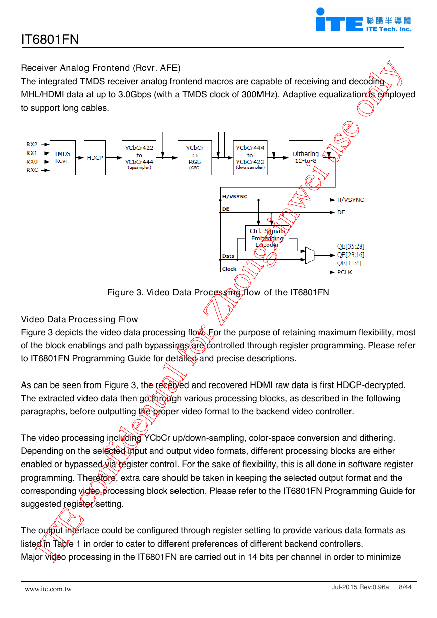
Figure 3. Video Data Processing flow of the IT6801FN
The video processing including YCbCr up/down-sampling, color-space conversion and dithering.
Depending on the selected input and output video formats, different processing blocks are either
As can be seen from Figure 3, the received and recovered HDMI raw data is first HDCP-decrypted.
The extracted video data then go through various processing blocks, as described in the following
Figure 3 depicts the video data processing flow. For the purpose of retaining maximum flexibility, most
of the block enablings and path bypassings are controlled through register programming. Please refer
enabled or bypassed via register control. For the sake of flexibility, this is all done in software register
programming. Therefore, extra care should be taken in keeping the selected output format and the
corresponding video processing block selection. Please refer to the IT6801FN Programming Guide for
paragraphs, before outputting the proper video format to the backend video controller.
The output interface could be configured through register setting to provide various data formats as
listed in Table 1 in order to cater to different preferences of different backend controllers.
Major video processing in the IT6801FN are carried out in 14 bits per channel in order to minimize
www.ite.com.tw
T8720F V0.7.1
Jul-2015 Rev:0.96a 8/44
Video Data Processing Flow
to IT6801FN Programming Guide for detailed and precise descriptions.
suggested register setting.
�




 2023年江西萍乡中考道德与法治真题及答案.doc
 2012年重庆南川中考生物真题及答案.doc
 2013年江西师范大学地理学综合及文艺理论基础考研真题.doc
 2020年四川甘孜小升初语文真题及答案I卷.doc
 2020年注册岩土工程师专业基础考试真题及答案.doc
 2023-2024学年福建省厦门市九年级上学期数学月考试题及答案.doc
 2021-2022学年辽宁省沈阳市大东区九年级上学期语文期末试题及答案.doc
 2022-2023学年北京东城区初三第一学期物理期末试卷及答案.doc
 2018上半年江西教师资格初中地理学科知识与教学能力真题及答案.doc
 2012年河北国家公务员申论考试真题及答案-省级.doc
 2020-2021学年江苏省扬州市江都区邵樊片九年级上学期数学第一次质量检测试题及答案.doc
 2022下半年黑龙江教师资格证中学综合素质真题及答案.doc