IEEE TRANSACTIONS ON MICROWAVE THEORY AND TECHNIQUES, VOL. 51, NO. 4, APRIL 2003
1395
Digital Receivers and Transmitters Using Polyphase
Filter Banks for Wireless Communications
Fredric J. Harris, Fellow, IEEE, Chris Dick, Member, IEEE, and Michael Rice, Senior Member, IEEE
Abstract—This paper provides a tutorial overview of multi-
channel wireless digital receivers and the relationships between
channel bandwidth, channel separation, and channel sample rate.
The overview makes liberal use of figures to support the under-
lying mathematics. A multichannel digital receiver simultaneously
down-convert a set of
frequency-division-multiplexed (FDM)
channels residing in a single sampled data signal stream. In a
similar way, a multichannel digital transmitter simultaneously
up-converts a number of baseband signals to assemble a set
of FDM channels in a single sampled data signal stream. The
polyphase filter bank has become the architecture of choice to
efficiently accomplish these tasks. This architecture uses three in-
teracting processes to assemble or to disassemble the channelized
signal set. In a receiver, these processes are an input commutator
to effect spectral folding or aliasing due to a reduction in sample
rate, a polyphase
-path filter to time align the partitioned
and resampled time series in each path, and a discrete Fourier
transform to phase align and separate the multiple baseband
aliases. In a transmitter, these same processes operate in a related
manner to alias baseband signals to high order Nyquist zones
while increasing the sample rate with the output commutator.
This paper presents a sequence of simple modifications to
sampled data structures based on analog prototype systems to
obtain the basic polyphase structure. We further discuss ways to
incorporate small modifications in the operation of the polyphase
system to accommodate secondary performance requirements.
MATLAB simulations of a 10-, 40-, and 50-channel resampling
receiver are included in the electronic version of this paper. An
animated version of the ten-channel resampling receiver illustrates
the time and frequency response of the filter bank when driven by
a slowly varying linear FM sweep.
Index Terms—Digital
radio, digital
receivers, equivalency theorem, multichannel digital receiver,
noble identity, polyphase filter bank.
channelizers, digital
MOTIVATION
R ADIO receivers and transmitters perform a sequence of
invertible signal transformations in order to communicate
through imperfect bandlimited channels. The transformations
applied to waveforms are associated with disjoint frequency
Manuscript received May 2, 2002.
F. J. Harris is with the Department of Electrical and Computer Engineering,
College of Engineering, San Diego State University, San Diego, CA 92182-1309
USA (e-mail: fred.harris@sdsu.edu).
C. Dick is with Xilinx, San Jose, CA 95124 USA (e-mail:
chris.dick@xilinx.com).
M. Rice is with the Department of Electrical Engineering, Brigham Young
University, Provo, UT 84601 USA.
This paper has supplementary downloadable material available at http://iee-
explore.ieee.org, provided by the authors. This includes six MATLAB script
files. These are standard m-files that will run under a MATLAB program. The
Signal Processing Toolbox is the only MATLAB Toolbox required to run these
script files. This material is 3.4 MB in size.
Digital Object Identifier 10.1109/TMTT.2003.809176
spans classically called baseband, IF, and RF. Early radios per-
formed the desired transformations using appropriate linear and
nonlinear lumped and distributed analog circuit elements.
The confluence of three technology areas has had pro-
found effect on the way we manipulate baseband and low
IF signals. Two of these areas, enabled by the transistor and
later by integrated circuits (ICs), are the analog-to-digital
converter (ADC) and digital-to-analog converter (DAC) and
the programmable microprocessor. The third technology area is
algorithm development by the digital signal processing (DSP)
community. These technologies coupled with an educated and
motivated work force led inexorably to insertion of DSP in
the signal-processing path of radio receiver and transmitter
systems.
Intel’s former CEO G. Moore [4] observed that the cost of
performing a specified processing task on an IC drops by a
factor of two every 18 months or, equivalently, the amount of
processing that can be performed at a fixed cost doubles every
18 months. This relationship, known as Moore’s law, appears
to be unique to the semiconductor industry. A similar cost-per-
formance curve does not exist for general circuit components A
consequence of Moore’s law is the migration from designs that
assemble and integrate sub-system to designs that are full sys-
tems on a chip (SOC).
An important participant in the semiconductor arena is the
field programmable gate array (FPGA) [5]. The FPGA con-
sists of a vast array of configurable logic tiles, multipliers, and
memory. This technology provides the signal-processing engi-
neer with the ability to construct a custom data path that is
tailored to the application at hand. FPGAs offer the flexibility
of instruction set digital signal processors while providing the
processing power and flexibility of an application-specific in-
tegrated circuit (ASIC). The FPGA enables significant design
cycle compression and time-to-market advantages, an impor-
tant consideration in an economic climate with ever-decreasing
market windows and short product life cycles.
DSP-based processing of baseband and low IF signals offer
cost and performance advantages related to manufacturability,
insensitivity to environment, ability to absorb design changes,
and ease of feature insertion for product evolution and differen-
tiability. The DSP segment of a radio enhances the radio while
reducing its cost, thus enabling larger market penetration, as
well as new market formation. DSP and RF and microwave com-
munication systems are tightly coupled.
The authors have written this paper to help the RF and mi-
crowave engineer acquire an understanding of the key work per-
formed by their DSP partners in pursuit of their common goal,
the design and production of competitive high-quality RF com-
munication and RF monitoring systems. We begin this paper
with a review of a standard architecture for analog transmitters
0018-9480/03$17.00 © 2003 IEEE
�
1396
IEEE TRANSACTIONS ON MICROWAVE THEORY AND TECHNIQUES, VOL. 51, NO. 4, APRIL 2003
Fig. 1. First-generation RF architecture of N -channel receiver.
Fig. 2. First-generation RF architecture of N -channel transmitter.
and receivers. Here, the interface between continuous and sam-
pled data is located at the end of the signal-processing path
and operates at the highest signal-to-noise ratio with the lowest
sample rate. We then present variants of the standard architec-
tures in which the operating conditions change to process sig-
nals at higher dynamic range and at higher sample rates. A
common variant of the high sample rate option is IF sampling.
High sample rate converters offer the option in a receiver to
acquire large segments of input bandwidth and absorb much of
the signal-processing tasks and functions in DSP algorithms.
The dual task of assembling large segments of bandwidth in a
transmitter is implied, but is not addressed here. The receiver
processing includes partitioning, filtering, translation, and de-
modulated. The remainder of this paper is restricted to a de-
scription of various techniques to accomplish single or multiple
channel extraction of signal bands from the bandwidth collected
by high-bandwidth converters.
I. INTRODUCTION
Base stations for cellular mobile communication systems [6]
offer an example of a radio receiver that must down-convert and
demodulate multiple simultaneous narrow-band RF channels.
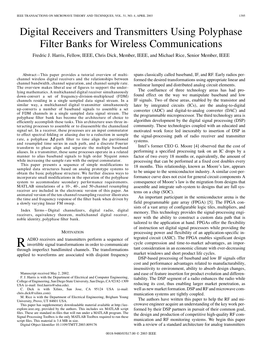
The traditional architecture of a radio receiver that performs
sets
this task is shown in Fig. 1. This architecture contains
of dual-conversion sub-receivers. Each receiver amplifies and
down-converts a selected RF channel to an IF filter that per-
forms initial bandwidth limiting.
The output of each IF filter is again down converted to
baseband by matched quadrature mixers that are followed by
matched baseband filters that perform final bandwidth control.
Each quadrature down-converted signal is then converted to
their digital representation by a pair of matched ADCs. The
output of the ADCs is processed by DSP engines that perform
the required synchronization, equalization, demodulation,
detection, and channel decoding.
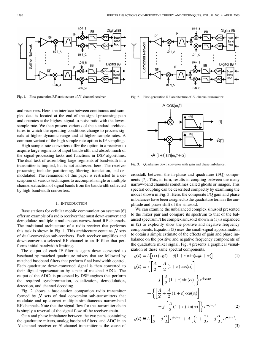
Fig. 2 shows a base-station companion radio transmitter
sets of dual conversion sub-transmitters that
formed by
modulate and up-convert multiple simultaneous narrow-band
RF channels. Note that the signal flow for the transmitter chain
is simply a reversal of the signal flow of the receiver chain.
Gain and phase imbalance between the two paths containing
the quadrature mixers, analog baseband filters, and ADC in an
-channel transmitter is the cause of
-channel receiver or
Fig. 3. Quadrature down converter with gain and phase imbalance.
crosstalk between the in-phase and quadrature (I/Q) compo-
nents [7]. This, in turn, results in coupling between the many
narrow-band channels sometimes called ghosts or images. This
spectral coupling can be described compactly by examining the
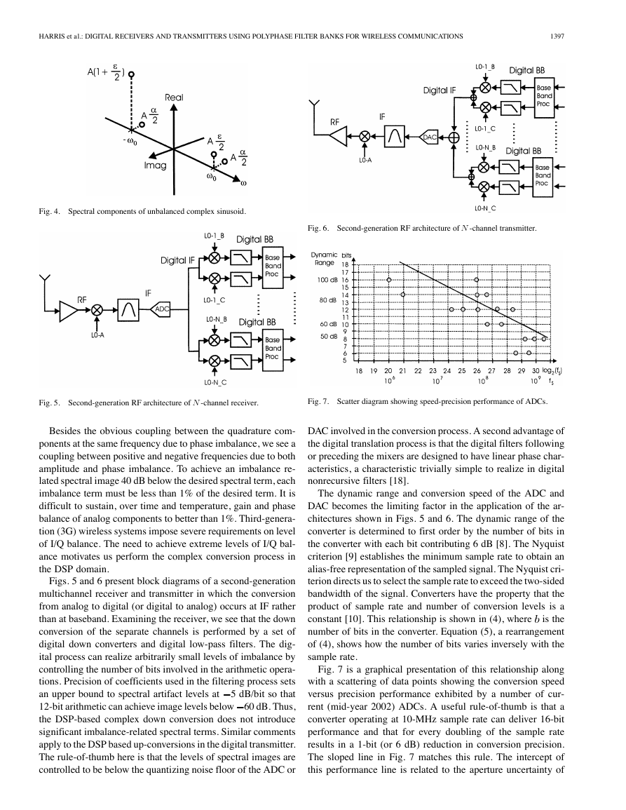
model shown in Fig. 3. Here, the composite I/Q gain and phase
imbalances have been assigned to the quadrature term as the am-
plitude and phase shift of the sinusoid.
We can examine the unbalanced complex sinusoid presented
to the mixer pair and compare its spectrum to that of the bal-
anced spectrum. The complex sinusoid shown in (1) is expanded
in (2) to explicitly show the positive and negative frequency
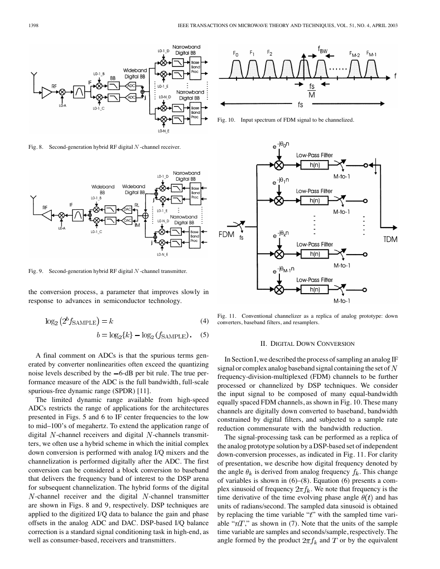
components. Equation (3) uses the small-signal approximation
to obtain a simple estimate of the effects of gain and phase im-
balance on the positive and negative frequency components of
the quadrature mixer signal. Fig. 4 presents a graphical visual-
ization of these same spectral components.
(1)
(2)
(3)
�
HARRIS et al.: DIGITAL RECEIVERS AND TRANSMITTERS USING POLYPHASE FILTER BANKS FOR WIRELESS COMMUNICATIONS
1397
Fig. 4. Spectral components of unbalanced complex sinusoid.
Fig. 6. Second-generation RF architecture of N -channel transmitter.
Fig. 5. Second-generation RF architecture of N -channel receiver.
Fig. 7. Scatter diagram showing speed-precision performance of ADCs.
Besides the obvious coupling between the quadrature com-
ponents at the same frequency due to phase imbalance, we see a
coupling between positive and negative frequencies due to both
amplitude and phase imbalance. To achieve an imbalance re-
lated spectral image 40 dB below the desired spectral term, each
imbalance term must be less than 1% of the desired term. It is
difficult to sustain, over time and temperature, gain and phase
balance of analog components to better than 1%. Third-genera-
tion (3G) wireless systems impose severe requirements on level
of I/Q balance. The need to achieve extreme levels of I/Q bal-
ance motivates us perform the complex conversion process in
the DSP domain.
Figs. 5 and 6 present block diagrams of a second-generation
multichannel receiver and transmitter in which the conversion
from analog to digital (or digital to analog) occurs at IF rather
than at baseband. Examining the receiver, we see that the down
conversion of the separate channels is performed by a set of
digital down converters and digital low-pass filters. The dig-
ital process can realize arbitrarily small levels of imbalance by
controlling the number of bits involved in the arithmetic opera-
tions. Precision of coefficients used in the filtering process sets
5 dB/bit so that
an upper bound to spectral artifact levels at
12-bit arithmetic can achieve image levels below 60 dB. Thus,
the DSP-based complex down conversion does not introduce
significant imbalance-related spectral terms. Similar comments
apply to the DSP based up-conversions in the digital transmitter.
The rule-of-thumb here is that the levels of spectral images are
controlled to be below the quantizing noise floor of the ADC or
DAC involved in the conversion process. A second advantage of
the digital translation process is that the digital filters following
or preceding the mixers are designed to have linear phase char-
acteristics, a characteristic trivially simple to realize in digital
nonrecursive filters [18].
The dynamic range and conversion speed of the ADC and
DAC becomes the limiting factor in the application of the ar-
chitectures shown in Figs. 5 and 6. The dynamic range of the
converter is determined to first order by the number of bits in
the converter with each bit contributing 6 dB [8]. The Nyquist
criterion [9] establishes the minimum sample rate to obtain an
alias-free representation of the sampled signal. The Nyquist cri-
terion directs us to select the sample rate to exceed the two-sided
bandwidth of the signal. Converters have the property that the
product of sample rate and number of conversion levels is a
is the
constant [10]. This relationship is shown in (4), where
number of bits in the converter. Equation (5), a rearrangement
of (4), shows how the number of bits varies inversely with the
sample rate.
Fig. 7 is a graphical presentation of this relationship along
with a scattering of data points showing the conversion speed
versus precision performance exhibited by a number of cur-
rent (mid-year 2002) ADCs. A useful rule-of-thumb is that a
converter operating at 10-MHz sample rate can deliver 16-bit
performance and that for every doubling of the sample rate
results in a 1-bit (or 6 dB) reduction in conversion precision.
The sloped line in Fig. 7 matches this rule. The intercept of
this performance line is related to the aperture uncertainty of
�
1398
IEEE TRANSACTIONS ON MICROWAVE THEORY AND TECHNIQUES, VOL. 51, NO. 4, APRIL 2003
Fig. 8. Second-generation hybrid RF digital N -channel receiver.
Fig. 10.
Input spectrum of FDM signal to be channelized.
Fig. 9. Second-generation hybrid RF digital N -channel transmitter.
the conversion process, a parameter that improves slowly in
response to advances in semiconductor technology.
(4)
(5)
A final comment on ADCs is that the spurious terms gen-
erated by converter nonlinearities often exceed the quantizing
6-dB per bit rule. The true per-
noise levels described by the
formance measure of the ADC is the full bandwidth, full-scale
spurious-free dynamic range (SPDR) [11].
-channel receivers and digital
The limited dynamic range available from high-speed
ADCs restricts the range of applications for the architectures
presented in Figs. 5 and 6 to IF center frequencies to the low
to mid–100’s of megahertz. To extend the application range of
-channels transmit-
digital
ters, we often use a hybrid scheme in which the initial complex
down conversion is performed with analog I/Q mixers and the
channelization is performed digitally after the ADC. The first
conversion can be considered a block conversion to baseband
that delivers the frequency band of interest to the DSP arena
for subsequent channelization. The hybrid forms of the digital
transmitter
are shown in Figs. 8 and 9, respectively. DSP techniques are
applied to the digitized I/Q data to balance the gain and phase
offsets in the analog ADC and DAC. DSP-based I/Q balance
correction is a standard signal conditioning task in high-end, as
well as consumer-based, receivers and transmitters.
-channel receiver and the digital
-channel
Fig. 11. Conventional channelizer as a replica of analog prototype: down
converters, baseband filters, and resamplers.
II. DIGITAL DOWN CONVERSION
In Section I, we described the process of sampling an analog IF
signal or complex analog baseband signal containing the set of
frequency-division-multiplexed (FDM) channels to be further
processed or channelized by DSP techniques. We consider
the input signal to be composed of many equal-bandwidth
equally spaced FDM channels, as shown in Fig. 10. These many
channels are digitally down converted to baseband, bandwidth
constrained by digital filters, and subjected to a sample rate
reduction commensurate with the bandwidth reduction.
is derived from analog frequency
The signal-processing task can be performed as a replica of
the analog prototype solution by a DSP-based set of independent
down-conversion processes, as indicated in Fig. 11. For clarity
of presentation, we describe how digital frequency denoted by
. This change
the angle
of variables is shown in (6)–(8). Equation (6) presents a com-
. We note that frequency is the
plex sinusoid of frequency
and has
time derivative of the time evolving phase angle
units of radians/second. The sampled data sinusoid is obtained
by replacing the time variable “ ” with the sampled time vari-
,” as shown in (7). Note that the units of the sample
able “
time variable are samples and seconds/sample, respectively. The
or by the equivalent
angle formed by the product
and
�
HARRIS et al.: DIGITAL RECEIVERS AND TRANSMITTERS USING POLYPHASE FILTER BANKS FOR WIRELESS COMMUNICATIONS
1399
Fig. 13. kth channel of conventional channelizer.
Fig. 14. Conceptual digital filter: coefficients and data registers, multipliers,
and adders.
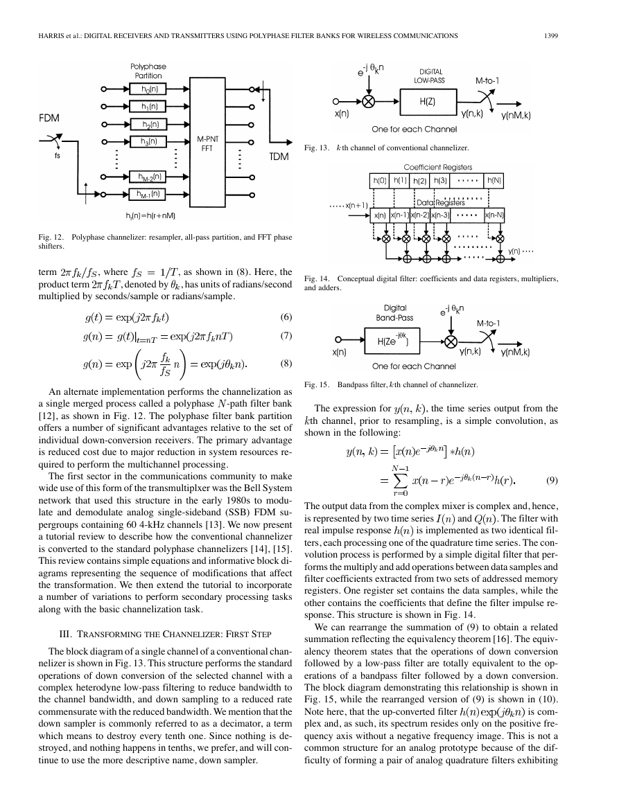
Fig. 12. Polyphase channelizer: resampler, all-pass partition, and FFT phase
shifters.
term
product term
multiplied by seconds/sample or radians/sample.
, as shown in (8). Here, the
, has units of radians/second
, where
, denoted by
(6)
(7)
(8)
An alternate implementation performs the channelization as
-path filter bank
a single merged process called a polyphase
[12], as shown in Fig. 12. The polyphase filter bank partition
offers a number of significant advantages relative to the set of
individual down-conversion receivers. The primary advantage
is reduced cost due to major reduction in system resources re-
quired to perform the multichannel processing.
The first sector in the communications community to make
wide use of this form of the transmultiplxer was the Bell System
network that used this structure in the early 1980s to modu-
late and demodulate analog single-sideband (SSB) FDM su-
pergroups containing 60 4-kHz channels [13]. We now present
a tutorial review to describe how the conventional channelizer
is converted to the standard polyphase channelizers [14], [15].
This review contains simple equations and informative block di-
agrams representing the sequence of modifications that affect
the transformation. We then extend the tutorial to incorporate
a number of variations to perform secondary processing tasks
along with the basic channelization task.
III. TRANSFORMING THE CHANNELIZER: FIRST STEP
The block diagram of a single channel of a conventional chan-
nelizer is shown in Fig. 13. This structure performs the standard
operations of down conversion of the selected channel with a
complex heterodyne low-pass filtering to reduce bandwidth to
the channel bandwidth, and down sampling to a reduced rate
commensurate with the reduced bandwidth. We mention that the
down sampler is commonly referred to as a decimator, a term
which means to destroy every tenth one. Since nothing is de-
stroyed, and nothing happens in tenths, we prefer, and will con-
tinue to use the more descriptive name, down sampler.
Fig. 15. Bandpass filter, kth channel of channelizer.
The expression for
, the time series output from the
th channel, prior to resampling, is a simple convolution, as
shown in the following:
(9)
and
The output data from the complex mixer is complex and, hence,
. The filter with
is represented by two time series
is implemented as two identical fil-
real impulse response
ters, each processing one of the quadrature time series. The con-
volution process is performed by a simple digital filter that per-
forms the multiply and add operations between data samples and
filter coefficients extracted from two sets of addressed memory
registers. One register set contains the data samples, while the
other contains the coefficients that define the filter impulse re-
sponse. This structure is shown in Fig. 14.
We can rearrange the summation of (9) to obtain a related
summation reflecting the equivalency theorem [16]. The equiv-
alency theorem states that the operations of down conversion
followed by a low-pass filter are totally equivalent to the op-
erations of a bandpass filter followed by a down conversion.
The block diagram demonstrating this relationship is shown in
Fig. 15, while the rearranged version of (9) is shown in (10).
is com-
Note here, that the up-converted filter
plex and, as such, its spectrum resides only on the positive fre-
quency axis without a negative frequency image. This is not a
common structure for an analog prototype because of the dif-
ficulty of forming a pair of analog quadrature filters exhibiting
�
1400
IEEE TRANSACTIONS ON MICROWAVE THEORY AND TECHNIQUES, VOL. 51, NO. 4, APRIL 2003
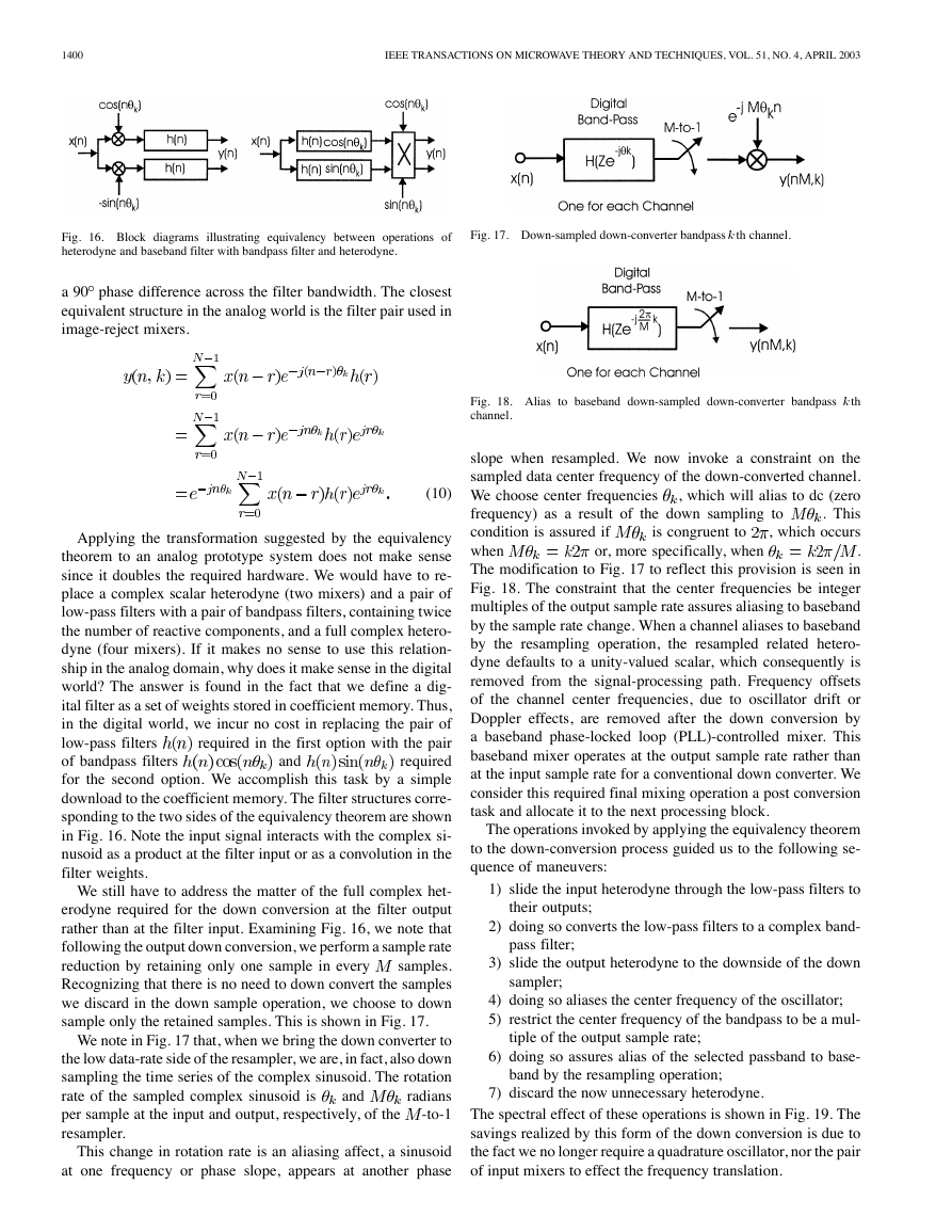
Fig. 16. Block diagrams illustrating equivalency between operations of
heterodyne and baseband filter with bandpass filter and heterodyne.
Fig. 17. Down-sampled down-converter bandpass kth channel.
a 90 phase difference across the filter bandwidth. The closest
equivalent structure in the analog world is the filter pair used in
image-reject mixers.
Fig. 18. Alias to baseband down-sampled down-converter bandpass kth
channel.
(10)
Applying the transformation suggested by the equivalency
theorem to an analog prototype system does not make sense
since it doubles the required hardware. We would have to re-
place a complex scalar heterodyne (two mixers) and a pair of
low-pass filters with a pair of bandpass filters, containing twice
the number of reactive components, and a full complex hetero-
dyne (four mixers). If it makes no sense to use this relation-
ship in the analog domain, why does it make sense in the digital
world? The answer is found in the fact that we define a dig-
ital filter as a set of weights stored in coefficient memory. Thus,
in the digital world, we incur no cost in replacing the pair of
required in the first option with the pair
low-pass filters
required
of bandpass filters
for the second option. We accomplish this task by a simple
download to the coefficient memory. The filter structures corre-
sponding to the two sides of the equivalency theorem are shown
in Fig. 16. Note the input signal interacts with the complex si-
nusoid as a product at the filter input or as a convolution in the
filter weights.
and
We still have to address the matter of the full complex het-
erodyne required for the down conversion at the filter output
rather than at the filter input. Examining Fig. 16, we note that
following the output down conversion, we perform a sample rate
samples.
reduction by retaining only one sample in every
Recognizing that there is no need to down convert the samples
we discard in the down sample operation, we choose to down
sample only the retained samples. This is shown in Fig. 17.
We note in Fig. 17 that, when we bring the down converter to
the low data-rate side of the resampler, we are, in fact, also down
sampling the time series of the complex sinusoid. The rotation
radians
rate of the sampled complex sinusoid is
-to-1
per sample at the input and output, respectively, of the
resampler.
and
This change in rotation rate is an aliasing affect, a sinusoid
at one frequency or phase slope, appears at another phase
is congruent to
or, more specifically, when
slope when resampled. We now invoke a constraint on the
sampled data center frequency of the down-converted channel.
, which will alias to dc (zero
We choose center frequencies
. This
frequency) as a result of the down sampling to
, which occurs
condition is assured if
.
when
The modification to Fig. 17 to reflect this provision is seen in
Fig. 18. The constraint that the center frequencies be integer
multiples of the output sample rate assures aliasing to baseband
by the sample rate change. When a channel aliases to baseband
by the resampling operation, the resampled related hetero-
dyne defaults to a unity-valued scalar, which consequently is
removed from the signal-processing path. Frequency offsets
of the channel center frequencies, due to oscillator drift or
Doppler effects, are removed after the down conversion by
a baseband phase-locked loop (PLL)-controlled mixer. This
baseband mixer operates at the output sample rate rather than
at the input sample rate for a conventional down converter. We
consider this required final mixing operation a post conversion
task and allocate it to the next processing block.
The operations invoked by applying the equivalency theorem
to the down-conversion process guided us to the following se-
quence of maneuvers:
1) slide the input heterodyne through the low-pass filters to
their outputs;
2) doing so converts the low-pass filters to a complex band-
pass filter;
3) slide the output heterodyne to the downside of the down
sampler;
4) doing so aliases the center frequency of the oscillator;
5) restrict the center frequency of the bandpass to be a mul-
tiple of the output sample rate;
6) doing so assures alias of the selected passband to base-
band by the resampling operation;
7) discard the now unnecessary heterodyne.
The spectral effect of these operations is shown in Fig. 19. The
savings realized by this form of the down conversion is due to
the fact we no longer require a quadrature oscillator, nor the pair
of input mixers to effect the frequency translation.
�
HARRIS et al.: DIGITAL RECEIVERS AND TRANSMITTERS USING POLYPHASE FILTER BANKS FOR WIRELESS COMMUNICATIONS
1401
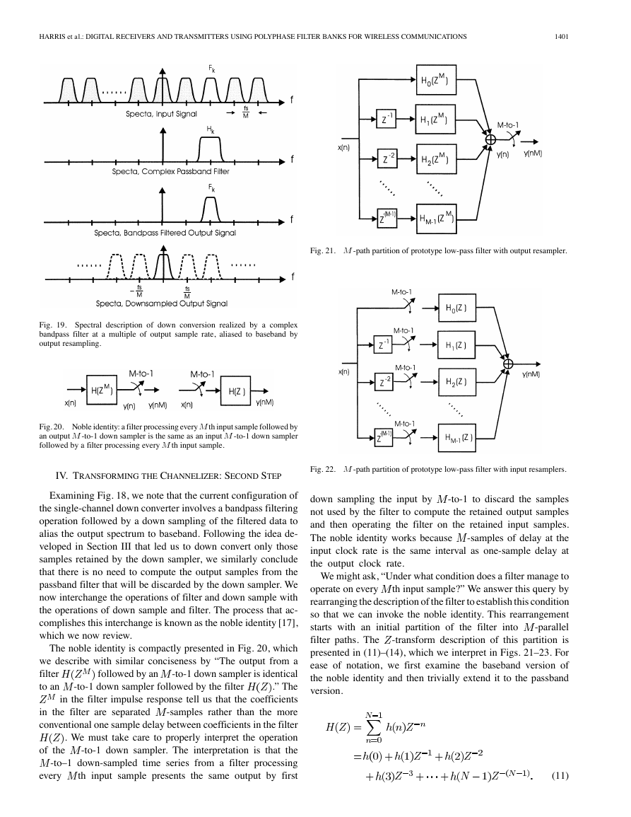
Fig. 19. Spectral description of down conversion realized by a complex
bandpass filter at a multiple of output sample rate, aliased to baseband by
output resampling.
Fig. 20. Noble identity: a filter processing every M th input sample followed by
an output M -to-1 down sampler is the same as an input M -to-1 down sampler
followed by a filter processing every M th input sample.
IV. TRANSFORMING THE CHANNELIZER: SECOND STEP
Examining Fig. 18, we note that the current configuration of
the single-channel down converter involves a bandpass filtering
operation followed by a down sampling of the filtered data to
alias the output spectrum to baseband. Following the idea de-
veloped in Section III that led us to down convert only those
samples retained by the down sampler, we similarly conclude
that there is no need to compute the output samples from the
passband filter that will be discarded by the down sampler. We
now interchange the operations of filter and down sample with
the operations of down sample and filter. The process that ac-
complishes this interchange is known as the noble identity [17],
which we now review.
followed by an
-to-1 down sampler followed by the filter
The noble identity is compactly presented in Fig. 20, which
we describe with similar conciseness by “The output from a
-to-1 down sampler is identical
filter
.” The
to an
in the filter impulse response tell us that the coefficients
-samples rather than the more
in the filter are separated
conventional one sample delay between coefficients in the filter
. We must take care to properly interpret the operation
-to-1 down sampler. The interpretation is that the
-to–1 down-sampled time series from a filter processing
th input sample presents the same output by first
of the
every
Fig. 21. M -path partition of prototype low-pass filter with output resampler.
Fig. 22. M -path partition of prototype low-pass filter with input resamplers.
down sampling the input by
-to-1 to discard the samples
not used by the filter to compute the retained output samples
and then operating the filter on the retained input samples.
-samples of delay at the
The noble identity works because
input clock rate is the same interval as one-sample delay at
the output clock rate.
We might ask, “Under what condition does a filter manage to
th input sample?” We answer this query by
operate on every
rearranging the description of the filter to establish this condition
so that we can invoke the noble identity. This rearrangement
-parallel
starts with an initial partition of the filter into
-transform description of this partition is
filter paths. The
presented in (11)–(14), which we interpret in Figs. 21–23. For
ease of notation, we first examine the baseband version of
the noble identity and then trivially extend it to the passband
version.
(11)
�
1402
IEEE TRANSACTIONS ON MICROWAVE THEORY AND TECHNIQUES, VOL. 51, NO. 4, APRIL 2003
We rewrite (13) in the traditional summation form, as shown
in (14), which describes the original polynomial as a sum of
delayed polynomials in
.
(14)
The block diagram reflecting this
-path partition of a re-
sampled digital filter is shown in Fig. 21. The output of the
separate filter
filter is the resampled sum of the output of the
-paths. We pull the resampler through the
stages along the
output summation element and down sample the separate out-
puts, only performing the output sum for the retained output
sample points. With the resamplers at the output of each filter,
th input sample, we are prepared to
which operates on every
invoke the noble identity and pull the resampler to the input side
of each filter stage. This is shown in Fig. 22. The input resam-
plers operate synchronously, all closing at the same clock cycle.
When the switches close, the signal delivered to the filter on the
top path is the current input sample. The signal delivered to the
filter one path down is the content of the one-stage delay line,
which, of course, is the previous input sample. Similarly, as we
-path partition, we find
traverse the successive paths of the
upon switch closure, that the th path receives a data sample de-
samples ago. We conclude that the interaction of the
livered
delay lines in each path with the set of synchronous switches
can be likened to an input commutator that delivers successive
-path filter. This interpreta-
samples to successive legs of the
tion is shown in Fig. 23.
We now complete the final steps of the transform that changes
-path down
a standard mixer down converter to a resampling
converter. We note and apply the frequency translation property
-transform [18]. This property is illustrated and stated
of the
in (15). Interpreting the relationship presented in (15), we note
, the impulse response of a baseband filter, has a
that, if
, the impulse
.
response of a passband filter, has a
Simply stated, we can convert a low-pass filter to a bandpass
filter by associating the complex heterodyne terms of the mod-
, then the sequence
-transform
-transform
Fig. 23. M -path partition of prototype low-pass filter with input path delays
and M -to-1 resamplers replaced by input commutator.
Anticipating the
-to-1 resampling, we partition the sum
shown in (11) to a sum of sums, as shown in (12) at the bottom
of this page. This partition maps a one-dimensional array of
) to a two-dimensional array.
weights (and index markers
This mapping is sometimes called lexicographic, for natural
order, a mapping that occurs in the Cooley–Tukey fast Fourier
transform (FFT). In this mapping, we load an array by columns,
but process the array by rows. In our example, the partition
successive terms
forms columns of length
-length
in the original sum, and continues to form adjacent
columns until we account for all the elements of the original
one-dimensional array shown in (12).
containing
, which we will denote
We note that the first row of the two-dimensional array is a
, a notation
polynomial in
to be interpreted as an addressing scheme to start at index 0
. The second row of the
and increment in stride of length
, is made into one
same array, while not a polynomial in
term and then identifying this
by factoring the common
. It is easy to see that each row of (12) can
row as
so that (12) can be rewritten in a
be described as
compact form, as shown in the following:
(13)
...
...
...
...
...
...
(12)
�


 2023年江西萍乡中考道德与法治真题及答案.doc
 2012年重庆南川中考生物真题及答案.doc
 2013年江西师范大学地理学综合及文艺理论基础考研真题.doc
 2020年四川甘孜小升初语文真题及答案I卷.doc
 2020年注册岩土工程师专业基础考试真题及答案.doc
 2023-2024学年福建省厦门市九年级上学期数学月考试题及答案.doc
 2021-2022学年辽宁省沈阳市大东区九年级上学期语文期末试题及答案.doc
 2022-2023学年北京东城区初三第一学期物理期末试卷及答案.doc
 2018上半年江西教师资格初中地理学科知识与教学能力真题及答案.doc
 2012年河北国家公务员申论考试真题及答案-省级.doc
 2020-2021学年江苏省扬州市江都区邵樊片九年级上学期数学第一次质量检测试题及答案.doc
 2022下半年黑龙江教师资格证中学综合素质真题及答案.doc