EEE525
Lab1
Mengbing Liang
EEE-525 VLSI Design
Lab1
1204252044
Mengbing Liang
2012/2/1
�
EEE525
Lab1
Mengbing Liang
Objective: Ring Oscillator analysis, interconnect modeling, power dissipation
estimation, impact of supply voltage.
Description:
The lab will be implemented in a technology that you have access to. This
technology will be used across the entire class, for all assignments and project.
It is preferred that the chosen technology will be a recent, high performance
technology; at the same time it should be a technology at which at least four
other students that you may work with during the project (your group) have
access to. On-line students may work in any technology, without the group
remark.
1. Every inverter in the ring oscillator has the NMOS transistor minimum
sized for the respective technology. The W and L of the PMOS transistor
equals the W and L of the NMOS transistor. The VDD for the ring oscillator
will be the nominal VDD voltage for the technology that you will use.
Ln=240nm
Lp=240nm
Wn=360nm
Wp=360nm
Vdd=2.5V
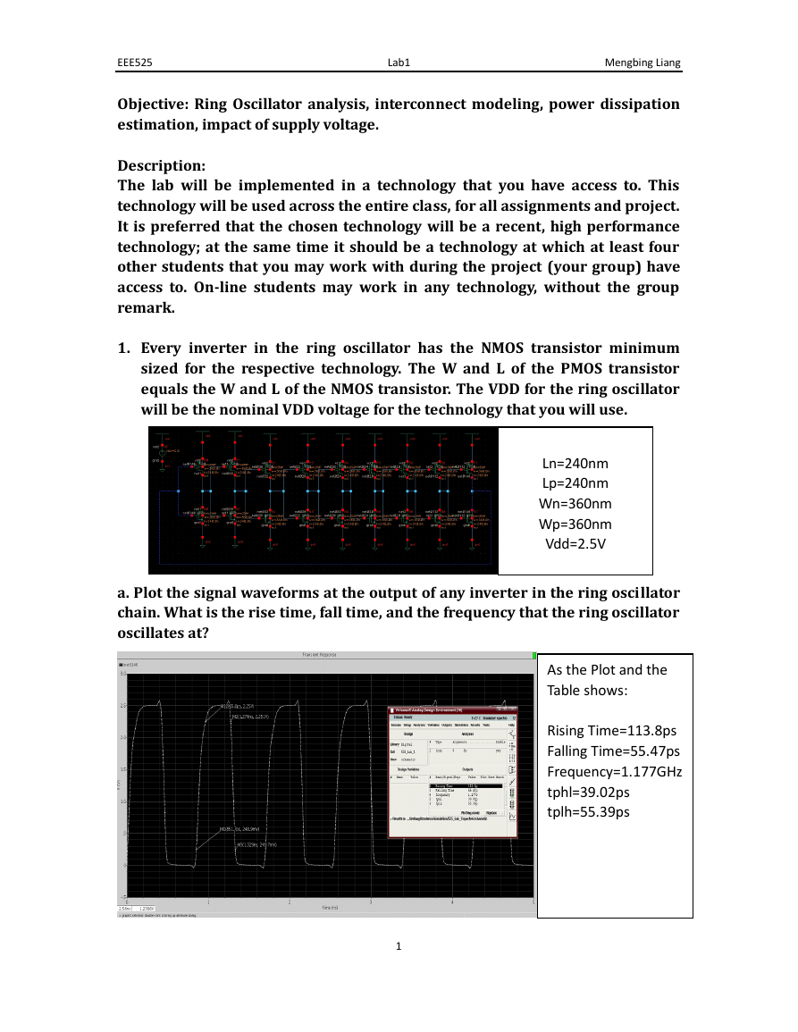
a. Plot the signal waveforms at the output of any inverter in the ring oscillator
chain. What is the rise time, fall time, and the frequency that the ring oscillator
oscillates at?
As the Plot and the
Table shows:
Rising Time=113.8ps
Falling Time=55.47ps
Frequency=1.177GHz
tphl=39.02ps
tplh=55.39ps
1
�
EEE525
Lab1
Mengbing Liang
b. What are your estimations for the load capacitance at the output of every
inverter, and for the R_ON of the devices?
Build a 2-inverter test circuit. The first stage is N9 and P9, and the second stage is
N11 and P11.
When Vin=0V, get the Cdd of N9 and P9,and the Cgg of N11 and P11 from the
browser.
When Vin=2.5V, get the Cdd of N9 and P9,and the Cgg of N11 and P11 from the
browser.
The Con=[(2.563+9.392+4.495+4.849)*10^(-16)+(5.153+6.099+1.99+7.481) *10^(-16)]/2=2.1011fF
2
�
EEE525
Lab1
Mengbing Liang
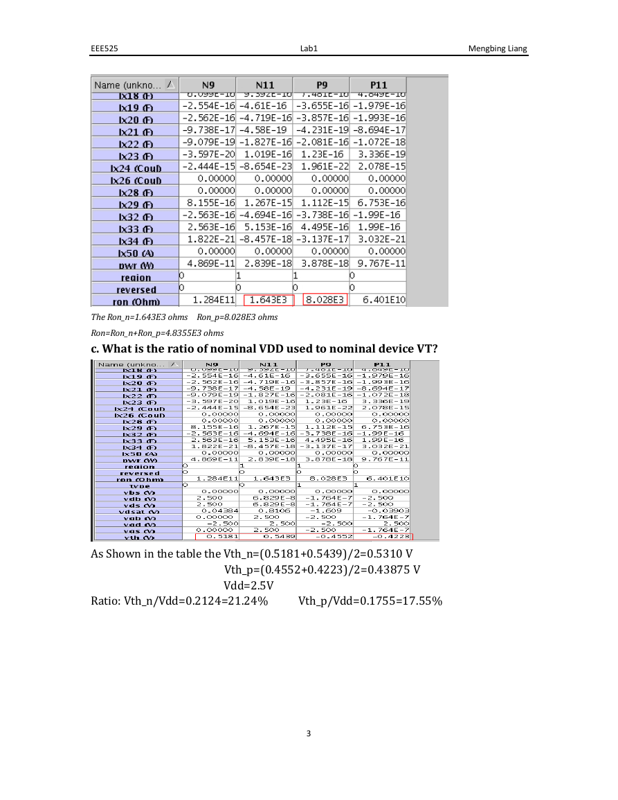
The Ron_n=1.643E3 ohms Ron_p=8.028E3 ohms
Ron=Ron_n+Ron_p=4.8355E3 ohms
c. What is the ratio of nominal VDD used to nominal device VT?
As Shown in the table the Vth_n=(0.5181+0.5439)/2=0.5310 V
Vth_p=(0.4552+0.4223)/2=0.43875 V
Vdd=2.5V
Ratio: Vth_n/Vdd=0.2124=21.24% Vth_p/Vdd=0.1755=17.55%
3
�
EEE525
Lab1
Mengbing Liang
2. While maintaining the NMOS transistors as at (1), increase the W of the
PMOS transistor until you achieve equal rise and fall times at the output of
an inverter (maintain same L).
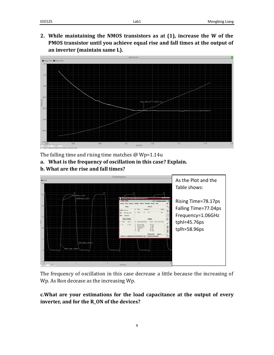
The falling time and rising time matches @ Wp=1.14u
a. What is the frequency of oscillation in this case? Explain.
b. What are the rise and fall times?
As the Plot and the
Table shows:
Rising Time=78.17ps
Falling Time=77.04ps
Frequency=1.06GHz
tphl=45.76ps
tplh=58.96ps
The frequency of oscillation in this case decrease a little because the increasing of
Wp. As Ron decease as the increasing Wp.
c.What are your estimations for the load capacitance at the output of every
inverter, and for the R_ON of the devices?
4
�
EEE525
Lab1
Mengbing Liang
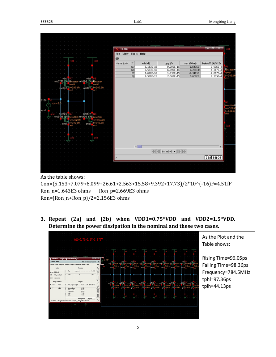
As the table shows:
Con=(5.153+7.079+6.099+26.61+2.563+15.58+9.392+17.73)/2*10^(-16)F=4.51fF
Ron_n=1.643E3 ohms Ron_p=2.669E3 ohms
Ron=(Ron_n+Ron_p)/2=2.156E3 ohms
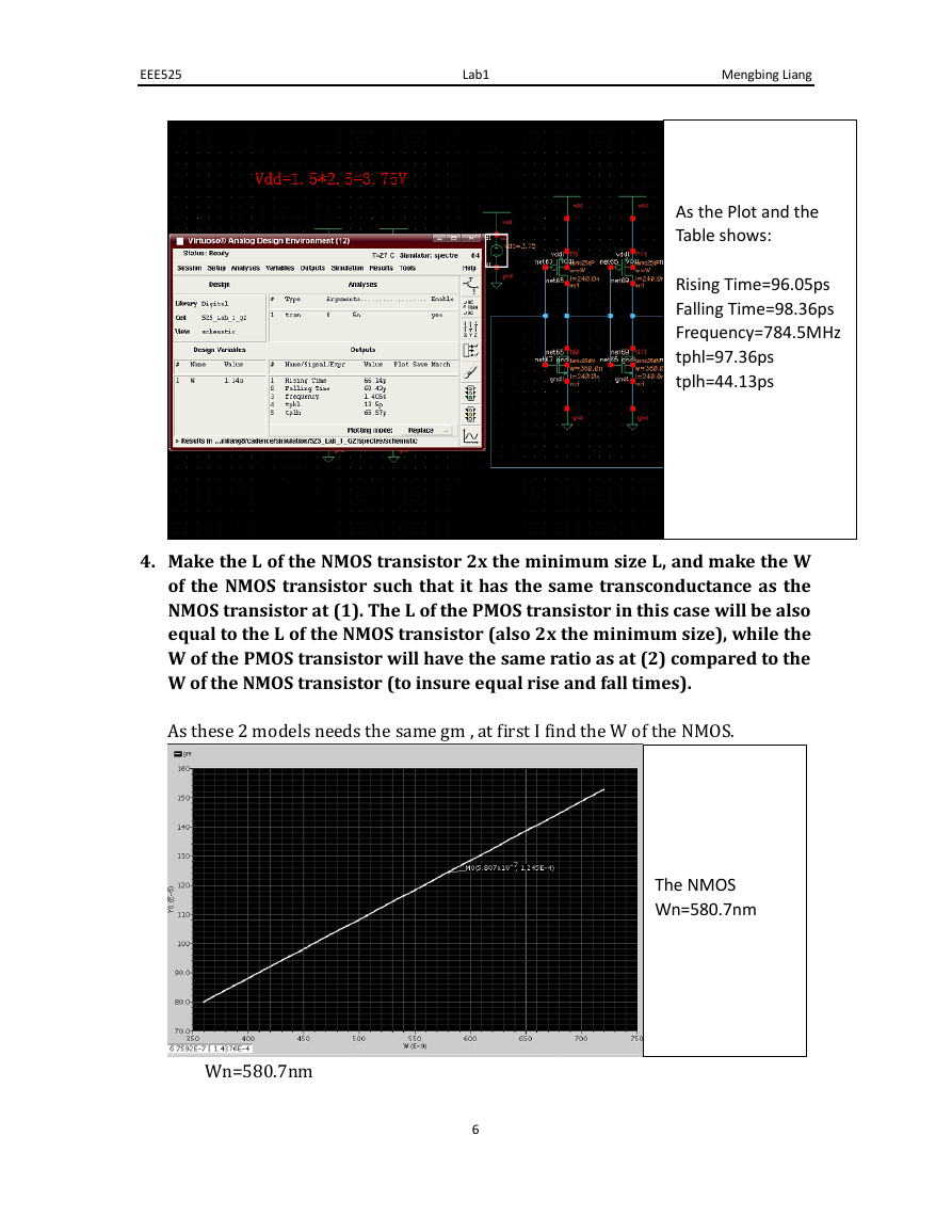
3. Repeat (2a) and (2b) when VDD1=0.75*VDD and VDD2=1.5*VDD.
Determine the power dissipation in the nominal and these two cases.
As the Plot and the
Table shows:
Rising Time=96.05ps
Falling Time=98.36ps
Frequency=784.5MHz
tphl=97.36ps
tplh=44.13ps
5
�
EEE525
Lab1
Mengbing Liang
As the Plot and the
Table shows:
Rising Time=96.05ps
Falling Time=98.36ps
Frequency=784.5MHz
tphl=97.36ps
tplh=44.13ps
4. Make the L of the NMOS transistor 2x the minimum size L, and make the W
of the NMOS transistor such that it has the same transconductance as the
NMOS transistor at (1). The L of the PMOS transistor in this case will be also
equal to the L of the NMOS transistor (also 2x the minimum size), while the
W of the PMOS transistor will have the same ratio as at (2) compared to the
W of the NMOS transistor (to insure equal rise and fall times).
As these 2 models needs the same gm , at first I find the W of the NMOS.
The NMOS
Wn=580.7nm
Wn=580.7nm
6
�
EEE525
Lab1
Mengbing Liang
a. What is the frequency of oscillation in this case? Explain.
b. What are the rise and fall times?
As the Plot and the
Table shows:
Rising Time=179.7ps
Falling Time=173.8ps
Frequency=413.5MHz
tphl=400ps
tplh=405.9ps
As both the L and W increase, the Con and Ron increase. So that obviously, the
Freaquency decreases and the delay increases.
What’s more, the Rising time and Falling time increase.
c. What are your estimations for the load capacitance at the output of
every inverter, and for the R_ON of the devices?
7
�




 2023年江西萍乡中考道德与法治真题及答案.doc
 2012年重庆南川中考生物真题及答案.doc
 2013年江西师范大学地理学综合及文艺理论基础考研真题.doc
 2020年四川甘孜小升初语文真题及答案I卷.doc
 2020年注册岩土工程师专业基础考试真题及答案.doc
 2023-2024学年福建省厦门市九年级上学期数学月考试题及答案.doc
 2021-2022学年辽宁省沈阳市大东区九年级上学期语文期末试题及答案.doc
 2022-2023学年北京东城区初三第一学期物理期末试卷及答案.doc
 2018上半年江西教师资格初中地理学科知识与教学能力真题及答案.doc
 2012年河北国家公务员申论考试真题及答案-省级.doc
 2020-2021学年江苏省扬州市江都区邵樊片九年级上学期数学第一次质量检测试题及答案.doc
 2022下半年黑龙江教师资格证中学综合素质真题及答案.doc