Features
Description
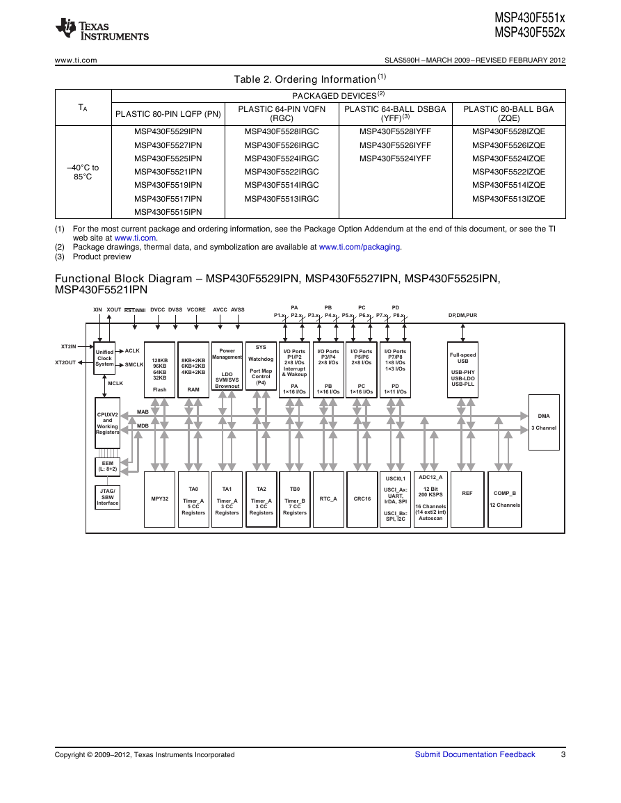
Functional Block Diagram – MSP430F5529IPN, MSP430F5527IPN, MSP430F5525IPN, MSP430F5521IPN
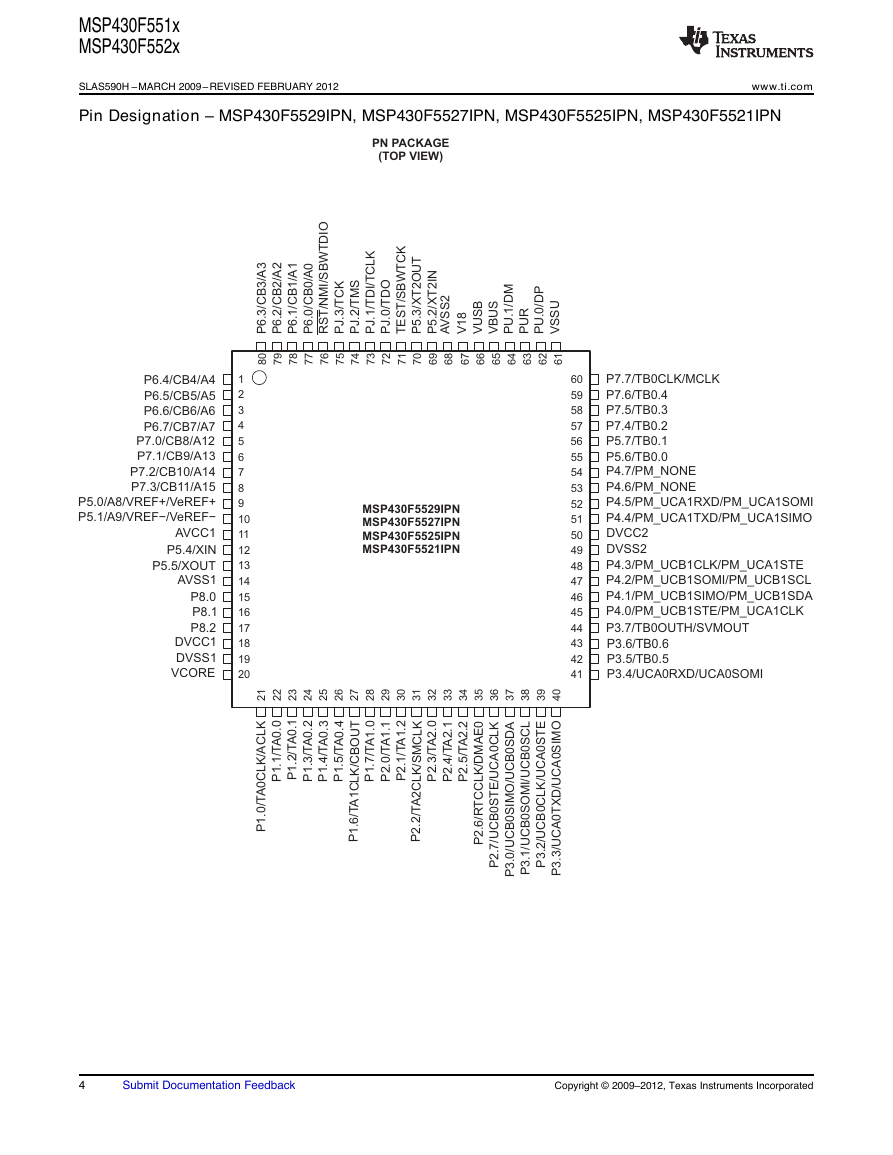
Pin Designation – MSP430F5529IPN, MSP430F5527IPN, MSP430F5525IPN, MSP430F5521IPN
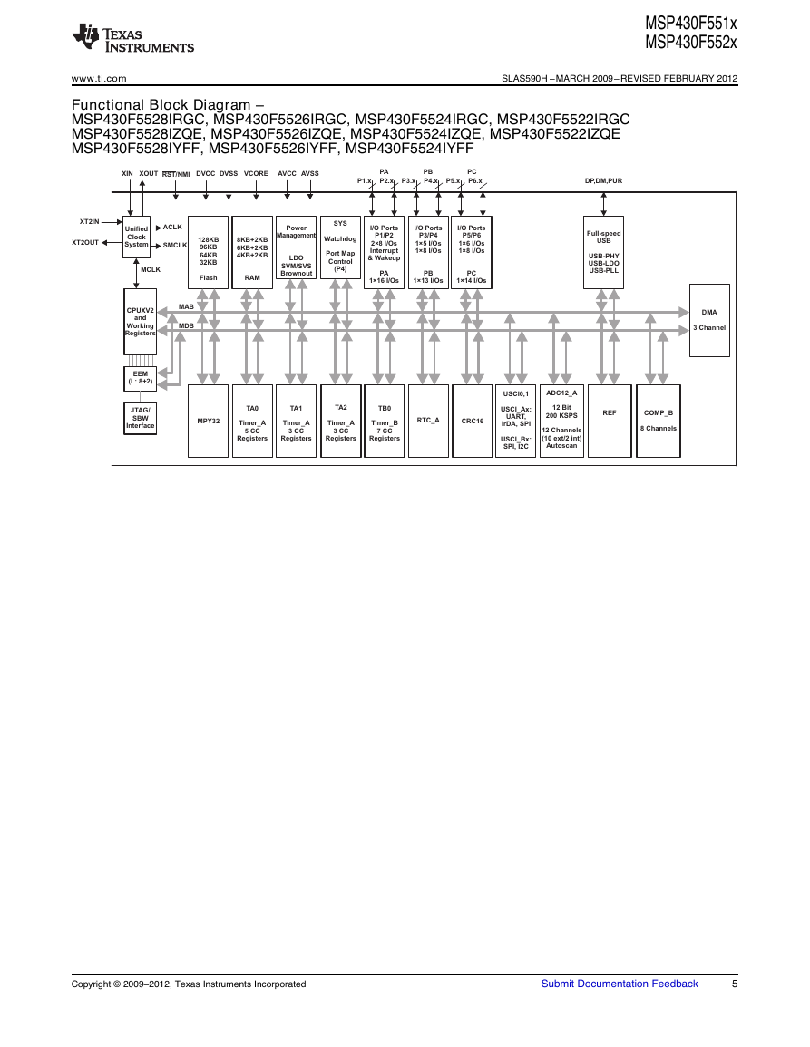
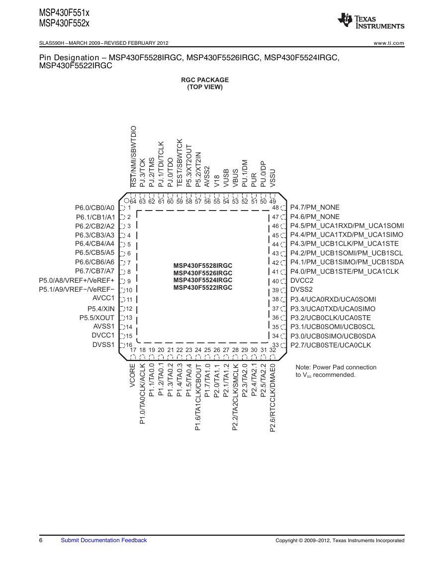
Functional Block Diagram – MSP430F5528IRGC, MSP430F5526IRGC, MSP430F5524IRGC, MSP430F5522IRGCMSP430F5528IZQE, MSP430F5526IZQE, MSP430F5524IZQE, MSP430F5522IZQEMSP430F5528IYFF, MSP430F5526IYFF, MSP430F5524IYFF
Pin Designation – MSP430F5528IRGC, MSP430F5526IRGC, MSP430F5524IRGC, MSP430F5522IRGC
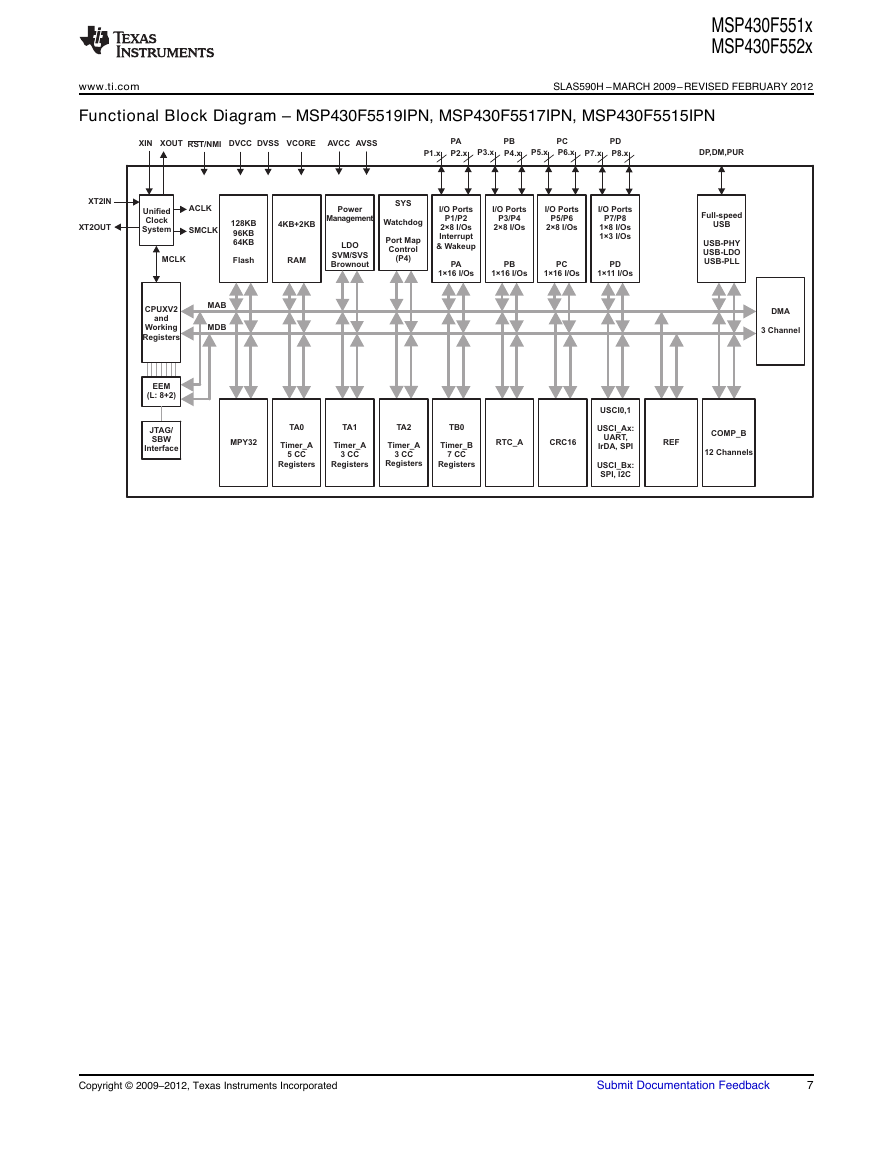
Functional Block Diagram – MSP430F5519IPN, MSP430F5517IPN, MSP430F5515IPN
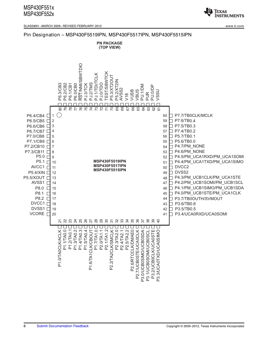
Pin Designation – MSP430F5519IPN, MSP430F5517IPN, MSP430F5515IPN
Functional Block Diagram – MSP430F5514IRGC, MSP430F5513IRGC, MSP430F5514IZQE, MSP430F5513IZQE
Pin Designation – MSP430F5514IRGC, MSP430F5513IRGC
Pin Designation – MSP430F5528IZQE, MSP430F5526IZQE, MSP430F5524IZQE, MSP430F5522IZQE, MSP430F5514IZQE, MSP430F5513IZQE
Pin Designation – MSP430F5528IYFF, MSP430F5526IYFF, MSP430F5524IYFF
Short-Form Description
CPU
Operating Modes
Interrupt Vector Addresses
Memory Organization
Bootstrap Loader (BSL)
USB BSL
UART BSL
JTAG Operation
JTAG Standard Interface
Spy-Bi-Wire Interface
Flash Memory
RAM Memory
Peripherals
Digital I/O
Port Mapping Controller
Oscillator and System Clock
Power Management Module (PMM)
Hardware Multiplier
Real-Time Clock (RTC_A)
Watchdog Timer (WDT_A)
System Module (SYS)
DMA Controller
Universal Serial Communication Interface (USCI)
TA0
TA1
TA2
TB0
Comparator_B
ADC12_A
CRC16
REF Voltage Reference
USB Universal Serial Bus
Embedded Emulation Module (EEM)
Peripheral File Map
Absolute Maximum Ratings
Thermal Packaging Characteristics
Recommended Operating Conditions
Electrical Characteristics
Active Mode Supply Current Into VCC Excluding External Current
Low-Power Mode Supply Currents (Into VCC) Excluding External Current
Schmitt-Trigger Inputs – General Purpose I/O(P1.0 to P1.7, P2.0 to P2.7, P3.0 to P3.7, P4.0 to P4.7)(P5.0 to P5.7, P6.0 to P6.7, P7.0 to P7.7, P8.0 to P8.2, PJ.0 to PJ.3, RST/NMI)
Inputs – Ports P1 and P2 (P1.0 to P1.7, P2.0 to P2.7)
Leakage Current – General Purpose I/O(P1.0 to P1.7, P2.0 to P2.7, P3.0 to P3.7, P4.0 to P4.7)(P5.0 to P5.7, P6.0 to P6.7, P7.0 to P7.7, P8.0 to P8.2, PJ.0 to PJ.3, RST/NMI)
Outputs – General Purpose I/O (Full Drive Strength)(P1.0 to P1.7, P2.0 to P2.7, P3.0 to P3.7, P4.0 to P4.7)(P5.0 to P5.7, P6.0 to P6.7, P7.0 to P7.7, P8.0 to P8.2, PJ.0 to PJ.3)
Outputs – General Purpose I/O (Reduced Drive Strength)(P1.0 to P1.7, P2.0 to P2.7, P3.0 to P3.7, P4.0 to P4.7)(P5.0 to P5.7, P6.0 to P6.7, P7.0 to P7.7, P8.0 to P8.2, PJ.0 to PJ.3)
Output Frequency – General Purpose I/O(P1.0 to P1.7, P2.0 to P2.7, P3.0 to P3.7, P4.0 to P4.7)(P5.0 to P5.7, P6.0 to P6.7, P7.0 to P7.7, P8.0 to P8.2, PJ.0 to PJ.3)
Typical Characteristics – Outputs, Reduced Drive Strength (PxDS.y = 0)
Typical Characteristics – Outputs, Full Drive Strength (PxDS.y = 1)
Crystal Oscillator, XT1, Low-Frequency Mode
Crystal Oscillator, XT2
Internal Very-Low-Power Low-Frequency Oscillator (VLO)
Internal Reference, Low-Frequency Oscillator (REFO)
DCO Frequency
PMM, Brown-Out Reset (BOR)
PMM, Core Voltage
PMM, SVS High Side
PMM, SVM High Side
PMM, SVS Low Side
PMM, SVM Low Side
Wake-Up From Low-Power Modes and Reset
Timer_A
Timer_B
USCI (UART Mode), Recommended Operating Conditions
USCI (UART Mode)
USCI (SPI Master Mode), Recommended Operating Conditions
USCI (SPI Master Mode)
USCI (SPI Slave Mode)
USCI (I2C Mode)
12-Bit ADC, Power Supply and Input Range Conditions
12-Bit ADC, Timing Parameters
12-Bit ADC, Linearity Parameters Using an External Reference Voltage or AVCC as Reference Voltage
12-Bit ADC, Linearity Parameters Using the Internal Reference Voltage
12-Bit ADC, Temperature Sensor and Built-In VMID
REF, External Reference
REF, Built-In Reference
Comparator_B
Ports PU.0 and PU.1
USB-Output Ports DP and DM
USB-Input Ports DP and DM
USB-PWR (USB Power System)
USB-PLL (USB Phase Locked Loop)
Flash Memory
JTAG and Spy-Bi-Wire Interface
Input/Output Schematics
Port P1, P1.0 to P1.7, Input/Output With Schmitt Trigger
Port P2, P2.0 to P2.7, Input/Output With Schmitt Trigger
Port P3, P3.0 to P3.7, Input/Output With Schmitt Trigger
Port P4, P4.0 to P4.7, Input/Output With Schmitt Trigger
Port P5, P5.0 and P5.1, Input/Output With Schmitt Trigger
Port P5, P5.2, Input/Output With Schmitt Trigger
Port P5, P5.3, Input/Output With Schmitt Trigger
Port P5, P5.4 and P5.5 Input/Output With Schmitt Trigger
Port P5, P5.6 to P5.7, Input/Output With Schmitt Trigger
Port P6, P6.0 to P6.7, Input/Output With Schmitt Trigger
Port P7, P7.0 to P7.3, Input/Output With Schmitt Trigger
Port P7, P7.4 to P7.7, Input/Output With Schmitt Trigger
Port P8, P8.0 to P8.2, Input/Output With Schmitt Trigger
Port PU.0/DP, PU.1/DM, PUR USB Ports
Port J, J.0 JTAG pin TDO, Input/Output With Schmitt Trigger or Output
Port J, J.1 to J.3 JTAG pins TMS, TCK, TDI/TCLK, Input/Output With Schmitt Trigger or Output
Device Descriptors (TLV)
Revision History



 2023年江西萍乡中考道德与法治真题及答案.doc
 2012年重庆南川中考生物真题及答案.doc
 2013年江西师范大学地理学综合及文艺理论基础考研真题.doc
 2020年四川甘孜小升初语文真题及答案I卷.doc
 2020年注册岩土工程师专业基础考试真题及答案.doc
 2023-2024学年福建省厦门市九年级上学期数学月考试题及答案.doc
 2021-2022学年辽宁省沈阳市大东区九年级上学期语文期末试题及答案.doc
 2022-2023学年北京东城区初三第一学期物理期末试卷及答案.doc
 2018上半年江西教师资格初中地理学科知识与教学能力真题及答案.doc
 2012年河北国家公务员申论考试真题及答案-省级.doc
 2020-2021学年江苏省扬州市江都区邵樊片九年级上学期数学第一次质量检测试题及答案.doc
 2022下半年黑龙江教师资格证中学综合素质真题及答案.doc