1454
IEEE JOURNAL OF SOLID-STATE CIRCUITS, VOL 24, NO 5, OCTOBER 1989
show that the total augmented area overhead is nearly 15 to 25
percent over the original PLA, but the chip yield can be im-
proved sigruficantly It should be mentioned that the signal
So = 0 is to isolate the shift registers from the orignal PLA’s
dunng the normal operation. Thus, the use of shift registers will
not affect the propagation delay in the design. In addition, since
the shft registers are used only for fault-hagnosis purposes, they
may possibly be shared by many PLA’s to reduce the chip area
overhead
Most existing testable PLA designs for fault detection employ
shift registers that are capable of only WRITE operation and
consume larger chip area than the proposed shift registers that
are capable of both WRITE and READ operations. Therefore: the
proposed shift register can be implemented for the testable PLA
design in less c h p area
clk
d
clk
REFERENCES
Master Latch
I
Slave Latch
(4
[1] C L Wey, M K V a , and F Lombardi, “On the design of a redundant
programmable logic array (RPLA),” IEEE J Solid-state Circuits, vol
SC-22, no 1, pp 114-117, Feb 1987
[2] C L Wey, “On yield considerations for the design of redundant pro-
grammable logic arrays,” IEEE Trans Comput a d e d Des , vol 7, no 4,
pp 528-535, Apr 1988
[3] N Wehn, M Glesner, K Caesar, P Mann, and A Roth, “A defect-
tolerant and fully testable PLA,” in Proc 2Sth ACM/IEEE Des Au-
tomut Conf (Anaheim, CA), June 1988, pp 22-27
[4] S Y Kuo and W K Fuchs, “Fault diagnosis and spare allocation for
yield enhancement in large reconfigurable PLA’s,” in Proc Int Test
C o n f , Sept 1987
[5] F Somenzi and S Gal, “Fault detection in programmable logic arrays,”
[6] R Tieuer, H FujlWara, and V K Agarwal, “Implementing a built-in
Proc IEEE, vol 74. no 5, pp 655-668, May 1986
self-test P I A design,” IEEE Des Test Comput , pp 37-48, Apr 1985
[7] C L Wey and T Y Chang, “Design of programmable logic arrays with
diagnosability,” Dept of Elec Eng , Micbgan State U n ~ v , Tech Rep ,
Oct 1988
Behavior Analysis of CMOS D Flip-Flops
H JONATHAN CHAO, MEMBER, IEEE,
AND CESAR A JOHNSTON
Absfruct -In
this paper, we analyze two D flip-flops (DFF’s) generally
considered to be the fastest (and most widely used), and compare their
speed performance and their robustness against clock skew when a two-
phase clocking scheme is applied. The effect of clock skew on their speed
and proper logic operation is analyzed,and verified with SPICE simulation.
I. INTRODUCTION
Synchronous pipelined structures have been extensively used to
obtain high-speed digital systems [l]. Pipelined structures are
used to reduce the propagation delay between two registers (D
flip flops, or DFF’s) where data and signal flow are synchronized
with clocks. The clock’s minimum period is constrained by the
DFF’s setup and delay times as well as the delay of any combina-
tional circuits between two DFF’s. Therefore, when building
synchronous pipelined structures, we want to reduce the DFF’s
setup and delay times as much as possible so that more stages of
combinational logic can be inserted between the pipelined regis-
ters.
Manuscript received February 3, 1989, remsed Apnl 11, 1989
The authors are with Bellcore. Morristown, NJ 07960
IEEE Log Number 8929744
1
,
Master Latch
I
Slave Latch
(b)
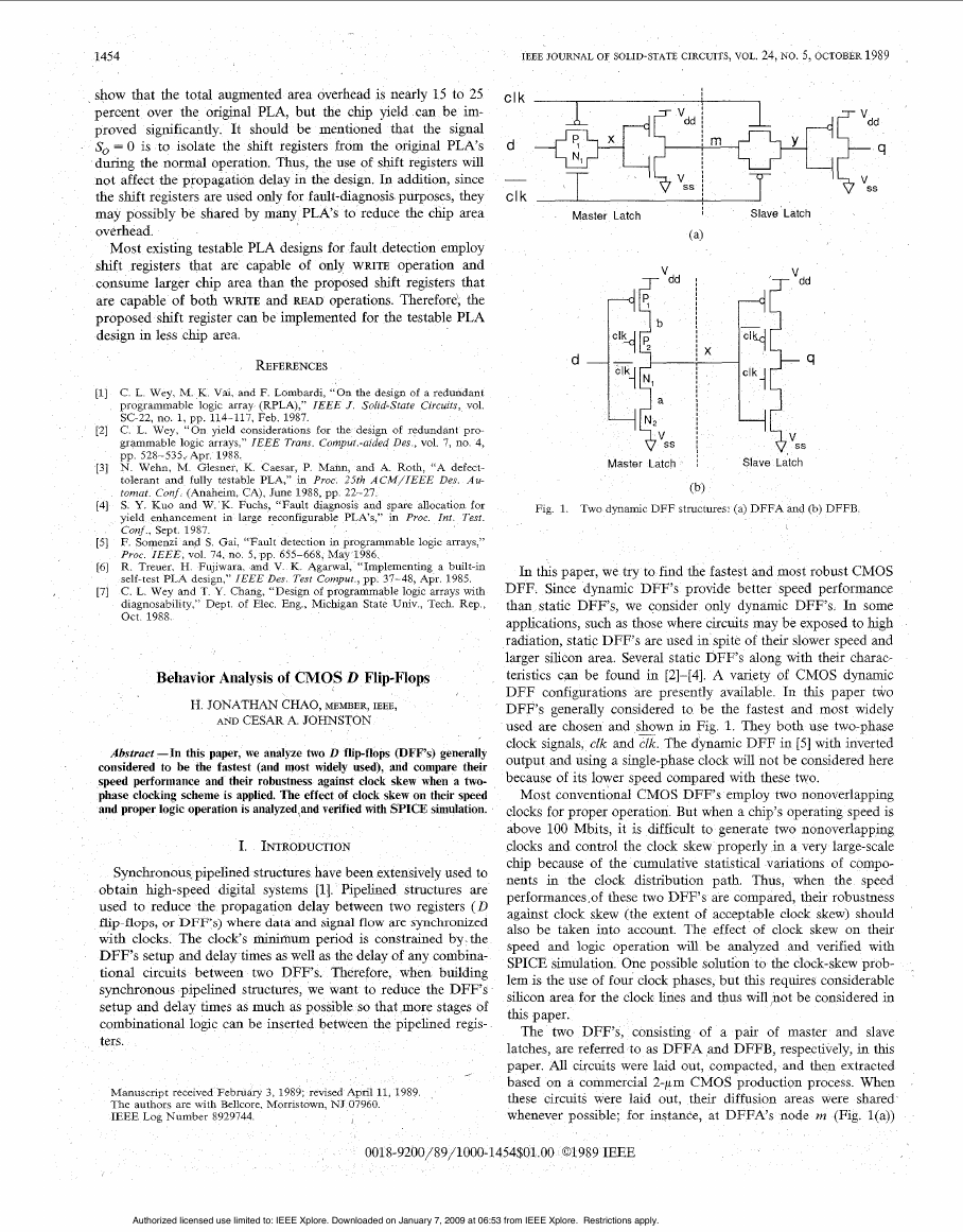
Fig 1 Two dynamic DFF structures (a) DFFA and (b) DFFB
In this paper, we try to find the fastest and most robust CMOS
DFF. Since dynamic DFF‘s provide better speed performance
than static DFF’s, we consider only dynamic DFF’s. In some
applications, such as those where circuits may be exposed to high
radiation, static DFF’s are used in spite of their slower speed and
larger silicon area. Several static DFF’s along with their charac-
teristics can be found in [2]-[4]. A variety of CMOS dynamic
DFF configurations are presently available In this paper two
DFF’s generally considered to be the fastest and most widely
used are chosen and shown in Fig 1. They both use two-phase
clock signals, clk and c2k. The dynamic DFF in [5] with inverted
output and using a single-phase clock will not be considered here
because of its lower speed compared with these two.
Most conventional CMOS DFF’s employ two nonoverlapping
clocks for proper operation But when a chip’s operating speed is
above 100 Mbits, it is difficult to generate two nonoverlapping
clocks and control the clock skew properly in a very large-scale
chip because of the cumulative statistical vanations of compo-
nents in the clock distribution path. Thus, when the speed
performances.of these two DFF’s are compared, their robustness
against clock skew (the extent of acceptable clock skew) should
also be taken into account. The effect of clock skew on their
speed and logic operation will be analyzed and verified with
SPICE simulation. One possible solution to the clock-skew prob-
lem is the use of four clock phases, but this requires considerable
silicon area for the clock lines and thus will ,not be considered in
this paper.
The two DFF’s, consisting of a pair of master and slave
latches, are referred to as DFFA and DFFB, respectively, in ths
paper. All circuits were laid out, compacted, and then extracted
based on a commercial 2-pm CMOS production process When
these circuits were laid out, their diffusion areas were shared
whenever possible; for instance, at DFFA’s node m (Fig. l(a))
001 8-9200/89/1000-1454$01 .OO 01 989 IEEE
Authorized licensed use limited to: IEEE Xplore. Downloaded on January 7, 2009 at 06:53 from IEEE Xplore. Restrictions apply.
�
IEEE JOURNAL OF SOLID-STATE CIRCUITS, VOL. 24, NO. 5, OCTOBER 1989
DFFl
Logic
DFF2
.
I
I
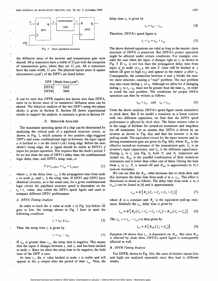
Fig. 2. Basic pipelined structure.
the diffusion areas of the inverter and transmission gate were
shared. All p transistors have a width of 27pm with the exception
of transmission gates, where they are 12 pm. All n transistors
have the same width, 12 pm. The physical layout areas in square
micrometers (pd) of the DFF‘s are listed below:
DFF I Mask Area (pm2)
DFFAl DFFB
5162
3888
It can be seen that DFFB requires less layout area than DFFA,
since in its layout most of its transistors’ diffusion areas can be
shared. The behavior analysis of the two DFF‘s using two-phase
clocks is given in Section 11. Section I11 shows experimental
results to support the analysis. A summary is given in Section IV.
11. BEHAVIOR ANALYSIS
The maximum operating speed of a chip can be determined by
analyzing the critical path of a pipelined structure circuit, as
shown in Fig. 2, which consists of two positive edge-triggered
DFF’s and some combinational logic in between. An input signal
a is latched to o on the clock‘s ( c k ) rising edge. Before the next
clock’s rising edge, the p signal should be stable at DFF2’s d
input for proper operation. This requires that the clock‘s period T
be no less than the sum of DFFl’s delay time, the combinational
logic delay time, and DFF2’s setup time, or
2 td.DFFl + top + ts.DFF2
(1)
where t, is the delay time, to, is the propagation time from node
o to node p , and t, is the setup time. If DFFl and DFF2 have
identical circuitry, as is the usual case, for a given combinational
logic circuit the pipelined structure speed is dependent on the
t, + t , value, also called the DFF’s speed figure and used to
compare different DFFs’ performance.
A. DFFA Timing Analysis
In order to latch the d value at node x in Fig. l(a) before clk
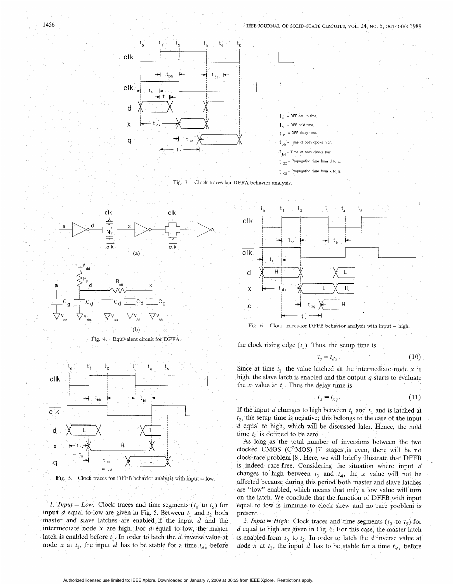
goes to low, the timings shown in Fig. 3 have to meet the
following condition:
delay time t, is given by
t , = th/, - txq.
Therefore, DFFA’s speed figure is
t, + t, = t,, + txq.
1455 .
( 4)
(5)
The above derived equations are valid as long as the master-slave
structure of DFFA is preserved. But DFFA’s proper operation
might be affected under certain conditions. For example, con-
sider the case when the input d changes right at t3 as shown in
Fig. 3. If thl is not less than the propagation delay time from
input d to node y(tdy), the new d value will be latched at y
goes to high (t,) and appear at the output q after t,.
before
Consequently, the connection between d and q breaks the mas-
ter-slave structure, causing a “race” problem. The race problem
may also occur during tl to t2. Although we allow for d changing
during t, to t,, t,, must not be greater than the time t,, in order
to avoid the race problem. The conditions for proper DFFA
operation can then be written as follows:
From the above analysis, DFFA’s speed figure seems insensitive
to clock skew. But if we model a transistor as a linear resistor
with two diffusion capacitors, we find that the DFFA speed
performance is aflected by clock skew. The linear resistor value is
in the range of kilohms for turned-on transistors and megohms
for off transistors. Let us assume that DFFA is driven by an
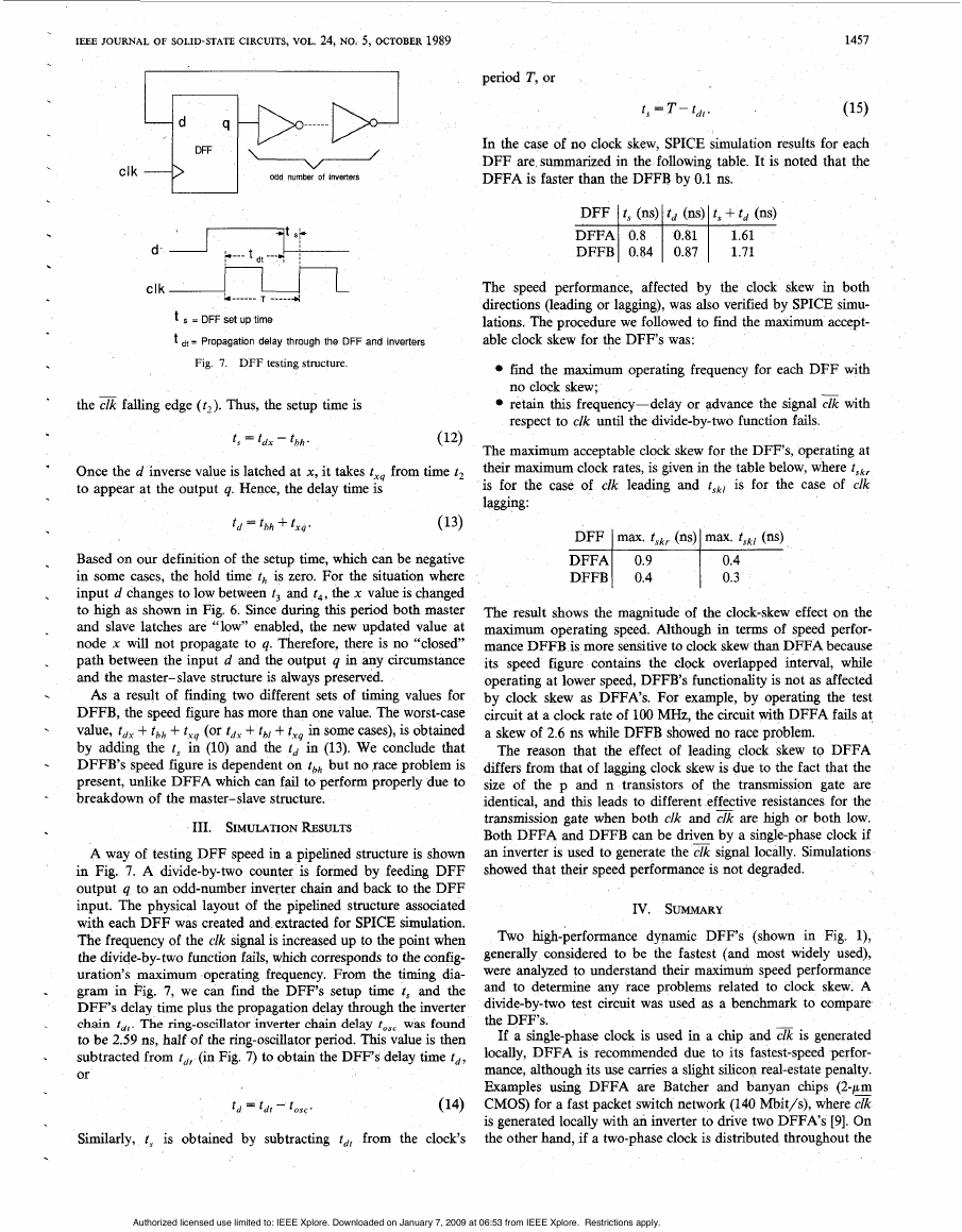
inverter as shown in Fig. 4(a) and that the inverter is in the
pull-up mode. The equivalent circuit for the input inverter and its
driving transmission gate are given by Fig. 4(b), where Reff is the
effective turned-on resistance of the transmission gate, C’
is an
inverter’s input capacitance, and C,
is the diffusion capacitance.
During to to t, (see Fig. 3), both Pl and NI transistors are
turned on; Reff is the parallel combination of their turned-on
resistances and is lower than either one of them. During the time
from t, to t,, Pl is turned off and Reff is approximate to N,’s
turn-on resistance.
We can see that the RefE value increases due to clock skew and
this increases the delay time from node d to x, tdx. This effect is
illustrated in detail as follows. The delay time from node a to d
( t u , ) can be found in [6] and is approximately
tu, = K [ R,(C, +C, + C, + C,)]
( 7)
where K is a constant and R, is the equivalent pull-up resis-
tance. Similarly the t,, delay time is given by
tax c K [ ~ p ( c d +C + C, + c g > + Reff(c, + ~ g > ] .
(8)
+ thh d t ,
The t,, ( = tu, - to,) is then given by
(2)
Thus, the setup time t, is given by
t , = td, - thh.
( 3)
If tbh is greater than t d l , the setup time is negative. This means
that the input d changes between tl and t, and has been latched
at node x. Since we allow the setup time to be negative, the hold
time of the DFF is zero.
At time t,, the d value latched at node x is stable and will
appear at the q output after the period of time txq. Thus, the
Equation (9) shows that tJ, is dependent on R,,,. But since Reef
is affected by clock skew, DFFA’s speed figure is consequently
affected as well.
B. DFFB Timing Analysis
For DFFB, shown in Fig. l(b), the cases of distinct inputs (low
and high) are analyzed separately since they lead to different
results.
Authorized licensed use limited to: IEEE Xplore. Downloaded on January 7, 2009 at 06:53 from IEEE Xplore. Restrictions apply.
�
1456
IEEE JOURNAL OF SOLID-STATE CIRCUITS, VOL 24, NO 5, OCTOBER 1989
high
= Time of both clocks low
t
t dX = Propagation time from d to x
t xq = Propagation time from x io q
Fig 3 Clock traces for DFFA behawor analysis
;
clk
clk
i
clk
(b)
Fig 4 Equivalent circmt for DFFA
x 6 t d x *
~
L
E
H
-
-4 t,,
Fig 6 Clock traces for DFFB behavior analysis w t h input = h g h
the clock rising edge (t,). Thus, the setup time is
(10)
Since at time tl the value latched at the intermediate node x is
high, the slave latch is enabled and the output q starts to evaluate
the x value at tl. Thus the delay time is
t, = t,, .
td = txq
(11)
If the input d changes to high between t, and t, and is latched at
t,, the setup time is negative; this belongs to the case of the input
d equal to high, whch will be discussed later. Hence, the hold
time th is defined to be zero.
As long as the total number of inversions between the two
clocked CMOS (C2MOS) [7] stages,is even, there will be no
clock-race problem [8]. Here, we will briefly illustrate that DFFB
is indeed race-free. Considering the situation where input d
changes to high between t, and I,, the x value will not be
affected because during this period both master and slave latches
are “low” enabled, which means that only a low value will turn
on the latch. We conclude that the function of DFFB with input
equal to low is immune to clock skew and no race problem is
present.
2. Input = Hzgh: Clock traces and time segments (to to t
d equal to high are given in Fig. 6. For this case, the master latch
is enabled from to to t, In order to latch the d inverse value at
node x at t,, the input d has to be stable for a time t,, before
Fig 5 Clock traces for DFFB behawor analysls wlth input = low
t d
1. Input = Low: Clock traces and time segments (to to t s ) for
input d equal to low are given in Fig. 5. Betwe
master and slave latches are enabled if the
intermediate node x are high. For d equal to low, the master
latch is enabled before t,. In order to latch the d inverse value at
node x at t,, the input d has to be stable for a time td, before
Authorized licensed use limited to: IEEE Xplore. Downloaded on January 7, 2009 at 06:53 from IEEE Xplore. Restrictions apply.
�
IEEE JOURNAL OF SOLID-STATE CIRCUITS, VOL. 24, NO. 5, OCTOBER 1989
period T, or
t, = T - td, .
1457
(15)
clk
odd number of inverters
clk
the clk falling edge (tr). Thus, the setup time is
Once the d inverse value is latched at x, it takes t
xq
to appear at the output q. Hence, the delay time is
from time t ,
Based on our definition of the setup time, which can be negative
in some cases, the hold time t, is zero. For the situation where
input d changes to low between t3 and t,, the x value is changed
to high as shown in Fig. 6. Since during this period both master
and slave latches are “low” enabled, the new updated value at
node x will not propagate to q. Therefore, there is no “closed”
path between the input d and the output q in any circumstance
and the master-slave structure is always preserved.
As a result of finding two different sets of timing values for
DFFB, the speed figure has more than one value. The worst-case
value, t,, + thh + t,, (or t,, + th/ + txq in some cases), is obtained
by adding the t, in (10) and the t, in (13). We conclude that
DFFB’s speed figure is dependent on thh but no face problem is
present, unlike DFFA which can fail to perform properly due to
breakdown of the master-slave structure.
111. SIMULATION RESULTS
A way of testing DFF speed in a pipelined structure is shown
in Fig. 7. A divide-by-two counter is formed by feeding DFF
output q to an odd-number inverter chain and back to the DFF
input. The physical layout of the pipelined structure associated
with each DFF was created and extracted for SPICE simulation.
The frequency of the clk signal is increased up to the point when
the divide-by-two function fails, which corresponds to the config-
uration’s maximum operating frequency. From the timing dia-
gram in Fig. 7, we can find the DFF‘s setup time t, and the
DFF’s delay time plus the propagation delay through the inverter
chain tdr. The ring-oscillator inverter chain delay to,, was found
to be 2.59 ns, half of the ring-oscillator period. This value is then
subtracted from t,, (in Fig. 7) to obtain the DFF‘s delay time td,
or
Similarly, t, is obtained by subtracting t,, from the clock’s
In the case of no dock skew, SPICE simulation results for each
DFF are summarized in the following table. It is noted that the
DFFA is faster than the DFFB by 0.1 ns.
I 0.81 I
DFF I t~ (ns) I td (ns) I t~ + td (ns>
DFFAI 0.8
DFFB 0.84
1.61
1.71
0.87
The speed performance, affected by the clock skew in both
directions (leading or lagging), was also verified by SPICE simu-
lations. The procedure we followed to find the maximum accept-
able clock skew for the DFF‘s was:
find the maximum operating frequency for each DFF with
no clock skew;
retain this frequency-delay or advance the signal clk with
respect to clk until the divide-by-two function fails.
The maximum acceptable clock skew for the DFF’s, operating at
their maximum clock rates, is given in the table below, where tskr
is for the case of clk leading and tskl is for the case of clk
lagging:
m t - x - j r
DFF max. tskr (ns) max. tskl (ns)
DFFB
0.4
0.3
The result shows the magnitude of the clock-skew effect on the
maximum operating speed. Although in terms of speed perfor-
mance DFFB is more sensitive to clock skew than DFFA because
its speed figure contains the clock overlapped interval, while
operating at lower speed, DFFB’s functionality is not as affected
by clock skew as DFFA’s. For example, by operating the test
circuit at a clock rate of 100 MHz, the circuit with DFFA fails at
a skew of 2.6 ns while DFFB showed no race problem.
The reason that the effect of leading clock skew t9 DFFA
differs from that of lagging clock skew is due to the fact that the
size of the p and n transistors of the transmission gate are
identical, and this leads to different effective resistances for the
transmission gate when both clk and clk are high or both low.
Both DFFA and DFFB can be driven by a single-phase clock if
an inverter is used to generate the clk signal locally. Simdations
showed that their speed performance is not degraded.
IV. S U m R Y
Two high-performance dynamic DFF‘s (shown in Fig. l),
generally considered to be the fastest (and most widely used),
were analyzed to understand their maximum speed performance
and to determine any race problems related to clock skew. A
divide-by-two test circuit was used as a benchmark to compare
the DFF’s.
If a single-phase clock is used in a chip and clk is generated
locally, DFFA is recommended due to its fastest-speed perfor-
mance, although its use carries a slight silicon real-estate penalty.
Examples using DFFA are Batcher and banyan chips (2-pm
CMOS) for a fast packet switch network (140 Mbit/s), where clk
is generated locally with an inverter to drive two DFFA’s [9]. On
the other hand, if a two-phase clock is distributed throughout the
Authorized licensed use limited to: IEEE Xplore. Downloaded on January 7, 2009 at 06:53 from IEEE Xplore. Restrictions apply.
�
1458
entire chp, since the balance between clk and clk capacitive
loading is difficult to control, DFFA is not suggested for use
unless the designer can assure that the clock-skew amount is
bounded. Instead, DFFB is recommended because its logic oper-
ation is immune to clock skew and it offers a smaller silicon area.
. For example, DFFB’s have been successfully employed in a
SONET-like Framer chip (2-pm CMOS) [lo], which is applicable
in a broad-band ISDN to facilitate high-speed data interface at a
Inside the chip, clk and clk are
bit rate up to 210 Mhit/s
broadcast throughout the chip through a four-stage buffer, driv-
ing about at 10-pF capacitive load.
REFERENCES
IEEE JOURNAL OF SOLID-STATE CIRCUITS, VOL 24, NO. 5, OCTOBER 1989
’“out
I
I
I
I
/
/
0 0
7 Bits
8Bits
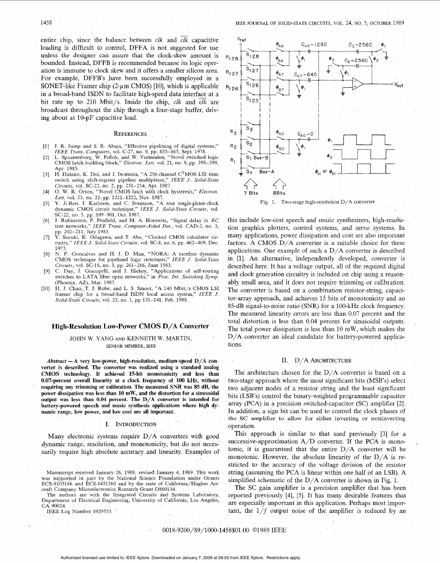
Fig 1 Two-stage high-resolution D/A converter
J R Jump and S R Ahuja, “Effective pipehmng of digital systems,”
IEEE Trans Computers, vol C-27, no 9, pp 855-865, Sept 1978
L Spaanenburg, W Pollok, and W Vermeulen, “Novel switched logc
CMOS latch building block,” Electron Lett vol 21, no 9, pp 398-399,
Apr 1985
H Hatano, K Dol, and J Iwamura, “A 256-channel C2MOS LSI time
switch using shift-register pipehne multiplexer,” IEEE J Solid-State
Circuits, vol SC-22, no 2, pp 251-254, Apr 1987
0 W R Orton, “Novel CMOS latch with clock hysteresis,” E!ectron
Lett vol 23, no 23, pp 1221-1222, Nov 1987
Y Ji-Ren I Karlsson. and C Svensson, “A true single-ohase-clock
dynamic CMOS circuit techmque,” IEEE J Solid-State dircuits, vol
SC-22, no 5, pp 899-901, Oct 1987
J Rubinstein, P Penfield, and M A Horowitz, “Signal delay in RC
tree networks,” IEEE Trans Computer-Aided D e s , vol CAD-2, no 3,
pp 202-211, July 1983
Y Suzuki, K Odagawa, and T Abe, “Clocked CMOS calculator cir-
cuitry,” IEEE J Solid-Stute Circuits, vol SC-8, no 6, pp 462-469, Dec
1973
N F Goncalves and H J D Man, “NORA A racefree d y n m c
CMOS technique for pipelined logic structures,” IEEE J Solid-State
Circuits, vol SC-18, no 3, pp 261-266, June 1983
C Day, J Giacopelli, and J Hickey, “ApplicaQons of self-routing
switches to LATA fiber ootic networks.” in Proc Int Switchine S V ~ D
(Phoenix, U), Mar 1987‘
H J Chao, T J Robe, and L S Smoot, “A 140 Mbit/s CMOS LSI
framer chip for a broad-band ISDN local access system,’’ IEEE J
Solid-Stat; Circuits, vol 23, no 1, pp 131-141, Feb 1988
-
,
/
High-Resolution Low-Power CMOS D/A Converter
JOHN W YANG AND KENNETH W MARTIN,
SENIOR MEMBER, IEEE
Abstract -A very low-power, high-resolution, medium-speed D/A con-
verter is described. The converter was realized using a standard analog
CMOS technology. It achieved 15-bit monotonicity and less than
0.07-percent overall linearity at a clock frequency of 100 kHz, without
requiring any trimming or calibration. The measured SNR was 85 dB, the
power dissipation was less than 10 mW, and the distortion for a sinusoidal
output was less than 0.04 percent. The D/A converter is intended for
battery-powered speech and music synthesis applications where high dy-
namic range, low power, and low cost are all important.
I. INTRODUCTION
Many electromc systems require D/A converters with good
dynamic range, resolution, and monotonicity, but do not neces-
sarily require high absolute accuracy and linearity. Examples of
Manuscript received January 26, 1988, revised January 4, 1989 This work
was supported in part by the National Science Foundahon under Grants
ECS-8105166 and ECS-8451260 and by the state of C&forma/Hughes A r -
craft Company Microelectronics Research Grant D860134
The authors are with the Integrated Circmts and Systems Laboratory,
Department of Electrical Engineenng, Umversity of Califorma, Los Angeles,
CA 90024
IEEE Log Number 8929553 ’
this include low-cost speech and music synthesizers, high-resolu-
tion graphics plotters, control systems, and servo systems. In
many applicabons, power dissipation and cost are also important
factors. A CMOS D/A converter is a suitable choice for these
applications. One example of such a D/A converter is described
in [l]. An alternative, independently developed, converter is
described here. It has a voltage output, all of the required diptal
and clock generation circuitry is included on chip using a reason-
ably small area, and it does not require trimming or calibration.
The converter is based on a combinabon resistor-stnng, capaci-
tor-array approach, and achieves 15 bits of monotonicity and an
85-dB signal-to-noise ratio (SNR) for a 100-kHz clock frequency.
The measured hnearity errors are less than 0.07 percent and the
total distortion is less than 004 percent for sinusoidal outputs
The total power dissipation is less than 10 mW, which makes the
D/A converter an ideal candidate for battery-powered applica-
tions.
,
11. D/A ARCHITECTURE
The architecture chosen for the D/A converter is based on a
two-stage approach where the most significant bits (MSB’s) select
two adjacent nodes of a resistor string and the least significant
bits (LSB’s) control the binary-weighted programmable capacitor
array (PCA) in a precision switched-capacitor (SC) amphfier [2].
In addition, a sign bit can be used to control the clock phases of
amphfier to allow for either inverting or noninverting
operation.
This approach is similar to that used previously [3] for a
successive-approximation A/D converter. If the PCA is mono-
tonic, it is guaranteed that the entire D/A converter will be
monotonic. However, the absolute linearity of the D/A is re-
stricted to the accuracy of the voltage division of the resistor
string (assuming the PCA is linear within one half of an LSB). A
simplified schematic of the D/A converter is shown in Fig. 1.
The SC gain amplifier is a precision amplifier that has been
reported prevlously [4], [5]. It has many desirable features that
are especially important in this application. Perhaps most impor-
tant, the l/f output noise of the amplifier is reduced by an
0018-9200/89/1000-1458$01.00 01989 IEEE
Authorized licensed use limited to: IEEE Xplore. Downloaded on January 7, 2009 at 06:53 from IEEE Xplore. Restrictions apply.
�


 2023年江西萍乡中考道德与法治真题及答案.doc
 2012年重庆南川中考生物真题及答案.doc
 2013年江西师范大学地理学综合及文艺理论基础考研真题.doc
 2020年四川甘孜小升初语文真题及答案I卷.doc
 2020年注册岩土工程师专业基础考试真题及答案.doc
 2023-2024学年福建省厦门市九年级上学期数学月考试题及答案.doc
 2021-2022学年辽宁省沈阳市大东区九年级上学期语文期末试题及答案.doc
 2022-2023学年北京东城区初三第一学期物理期末试卷及答案.doc
 2018上半年江西教师资格初中地理学科知识与教学能力真题及答案.doc
 2012年河北国家公务员申论考试真题及答案-省级.doc
 2020-2021学年江苏省扬州市江都区邵樊片九年级上学期数学第一次质量检测试题及答案.doc
 2022下半年黑龙江教师资格证中学综合素质真题及答案.doc