西安郵電學院
毕业设计(论文)
附件
(英文原文及译文)
系
专
班
别: 信息与控制
业: 测控技术与仪器
级: 测控 0302
学生姓名:
何 佳
导师姓名:
张 玲
起止时间:2007.3.20 至 2007.6.29
�
英文原文
Description
The AT89C51 is a low-power, high-performance CMOS 8-bit microcomputer with 4K bytes of
Flash Programmable and Erasable Read Only Memory (PEROM) and 128 bytes RAM. The device is
manufactured using Atmel’s high density nonvolatile memory technology and is compatible with the
industry standard MCS-51™ instruction set and pinout. The chip combines a versatile 8-bit CPU with
Flash on a monolithic chip, the Atmel AT89C51 is a powerful microcomputer which provides a highly
flexible and cost effective solution to many embedded control applications.
Features:
• Compatible with MCS-51™ Products
• 4K Bytes of In-System Reprogrammable Flash Memory
• Endurance: 1,000 Write/Erase Cycles
• Fully Static Operation: 0 Hz to 24 MHz
• Three-Level Program Memory Lock
• 128 x 8-Bit Internal RAM
• 32 Programmable I/O Lines
• Two 16-Bit Timer/Counters
• Six Interrupt Sources
• Programmable Serial Channel
• Low Power Idle and Power Down Modes
The AT89C51 provides the following standard features: 4K bytes of Flash, 128 bytes of RAM, 32
I/O lines, two 16-bit timer/counters, a five vector two-level interrupt architecture, a full duplex serial
port, on-chip oscillator and clock circuitry. In addition, the AT89C51 is designed with static logic for
operation down to zero frequency and supports two software selectable power saving modes. The Idle
Mode stops the CPU while allowing the RAM, timer/counters, serial port and interrupt system to
continue functioning. The Power Down Mode saves the RAM contents but freezes the oscillator
disabling all other chip functions until the next hardware reset.
�
Block Diagram
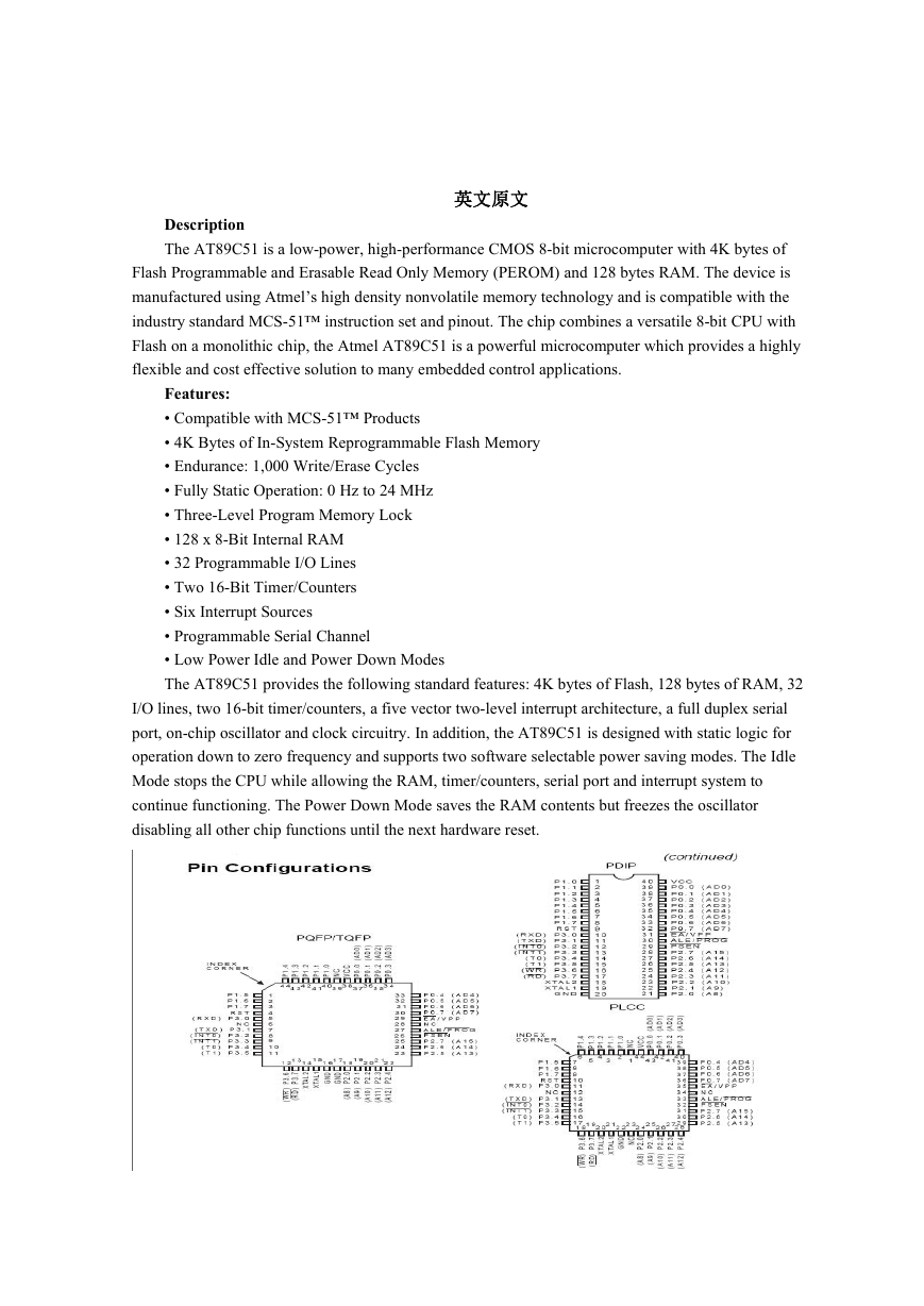
Pin Description:
VCC Supply voltage.
GND Ground.
Port 0
Port 0 is an 8-bit open drain bidirectional I/O port. As an output port each pin can sink eight TTL
inputs. When is are written to port 0 pins, the pins can be used as high impedance inputs.
Port 0 may also be configured to be the multiplexed loworder address/data bus during accesses to
external program and data memory. In this mode P0 has internal pullups.
Port 0 also receives the code bytes during Flash programming, and outputs the code bytes during
program verification. External pullups are required during program verification.
Port 1
Port 1 is an 8-bit bidirectional I/O port with internal pullups. The Port 1 output buffers can
sink/source four TTL inputs. When 1s are written to Port 1 pins they are pulled high by the internal
pullups and can be used as inputs. As inputs, Port 1 pins that are externally being pulled low will source
current (IIL) because of the internal pullups.
Port 1 also receives the low-order address bytes during Flash programming and verification.
�
Port 2
Port 2 is an 8-bit bidirectional I/O port with internal pullups. The Port 2 output buffers can
sink/source four TTL inputs. When 1s are written to Port 2 pins they are pulled high by the internal
pullups and can be used as inputs. As inputs, Port 2 pins that are externally being pulled low will source
current (IIL) because of the internal pullups.
Port 2 emits the high-order address byte during fetches from external program memory and
during accesses to external data memory that use 16-bit addresses (MOVX @ DPTR). In this
application it uses strong internal pull-ups when emitting 1s. During accesses to external data memory
that use 8-bit addresses (MOVX @ RI), Port 2 emits the contents of the P2 Special Function Register.
Port 2 also receives the high-order address bits and some control signals during Flash programming
and verification.
Port 3
Port 3 is an 8-bit bidirectional I/O port with internal pullups. The Port 3 output buffers can
sink/source four TTL inputs. When 1s are written to Port 3 pins they are pulled high by the internal
pullups and can be used as inputs. As inputs, Port 3 pins that are externally being pulled low will source
current (IIL) because of the pullups.
Port 3 also serves the functions of various special features of the AT89C51 as listed below:
Port pin
P3.0
P3.1
P3.2
P3.3
P3.4
P3.5
P3.6
P3.7
alternate functions
rxd (serial input port)
txd (serial output port)
^int0 (external interrupt0)
^int1 (external interrupt1)
t0 (timer0 external input)
t1 (timer1 external input)
^WR (external data memory write strobe)
^rd (external data memory read strobe)
Port 3 also receives
some control signals for
Flash programming and
verification.
RST
Reset input. A high on
this pin for two machine
cycles while the oscillator is
running resets the device.
ALE/PROG
Address Latch Enable output pulse for latching the low byte of the address during accesses to
external memory. This pin is also the program pulse input (PROG) during Flash programming.
In normal operation ALE is emitted at a constant rate of 1/6 the oscillator frequency, and may be
used for external timing or clocking purposes. Note, however, that one ALE pulse is skipped during
each access to external Data Memory.
If desired, ALE operation can be disabled by setting bit 0 of SFR location 8EH. With the bit set,
ALE is active only during a MOVX or MOVC instruction. Otherwise, the pin is weakly pulled high.
Setting the ALE-disable bit has no effect if the microcontroller is in external execution mode.
PSEN
Program Store Enable is the read strobe to external program memory.
When the AT89C51 is executing code from external program memory, PSEN is activated twice
each machine cycle, except that two PSEN activations are skipped during each access to external data
memory.
�
EA/VPP
External Access Enable. EA must be strapped to GND in order to enable the device to fetch code
from external program memory locations starting at 0000H up to FFFFH. Note, however, that if lock bit
1 is programmed, EA will be internally latched on reset.
EA should be strapped to VCC for internal program executions.
This pin also receives the 12-volt programming enable voltage(VPP) during Flash programming,
for parts that require 12-volt VPP.
XTAL1
Input to the inverting oscillator amplifier and input to the internal clock operating circuit.
XTAL2
Output from the inverting oscillator amplifier.
Oscillator Characteristics
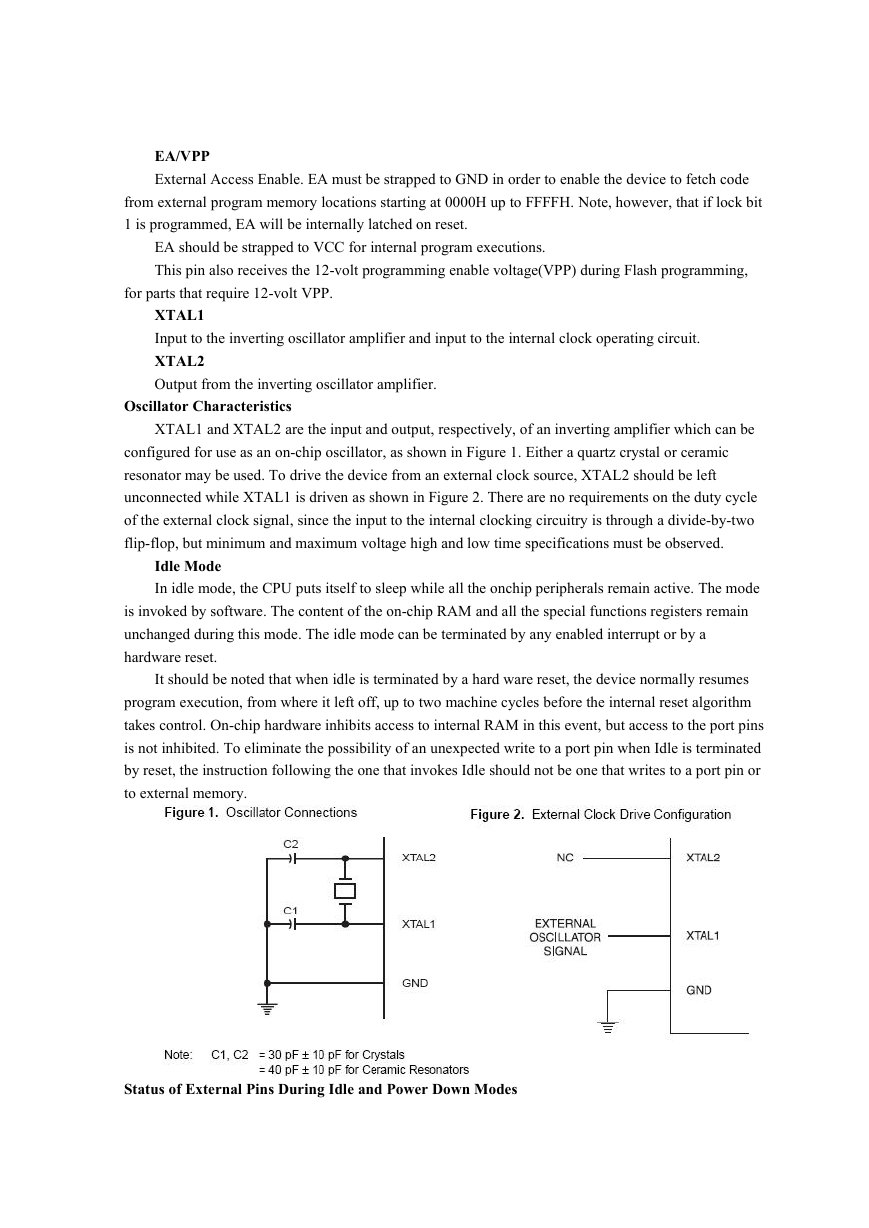
XTAL1 and XTAL2 are the input and output, respectively, of an inverting amplifier which can be
configured for use as an on-chip oscillator, as shown in Figure 1. Either a quartz crystal or ceramic
resonator may be used. To drive the device from an external clock source, XTAL2 should be left
unconnected while XTAL1 is driven as shown in Figure 2. There are no requirements on the duty cycle
of the external clock signal, since the input to the internal clocking circuitry is through a divide-by-two
flip-flop, but minimum and maximum voltage high and low time specifications must be observed.
Idle Mode
In idle mode, the CPU puts itself to sleep while all the onchip peripherals remain active. The mode
is invoked by software. The content of the on-chip RAM and all the special functions registers remain
unchanged during this mode. The idle mode can be terminated by any enabled interrupt or by a
hardware reset.
It should be noted that when idle is terminated by a hard ware reset, the device normally resumes
program execution, from where it left off, up to two machine cycles before the internal reset algorithm
takes control. On-chip hardware inhibits access to internal RAM in this event, but access to the port pins
is not inhibited. To eliminate the possibility of an unexpected write to a port pin when Idle is terminated
by reset, the instruction following the one that invokes Idle should not be one that writes to a port pin or
to external memory.
Status of External Pins During Idle and Power Down Modes
�
mode
idle
Idle
Power down
Power down
Program memory
ALE
internal
External
Internal
External
1
1
0
0
^psen
1
1
0
0
Port0
data
float
Data
float
Port1
data
Data
Data
data
Port2
data
data
Data
Data
Port3
Data
Data
Data
data
Power Down Mode
In the power down mode the oscillator is stopped, and the instruction that invokes power down is
the last instruction executed. The on-chip RAM and Special Function Registers retain their values until
the power down mode is terminated. The only exit from power down is a hardware reset. Reset
redefines the SFRs but does not change the on-chip RAM. The reset should not be activated before
VCC is restored to its normal operating level and must be held active long enough to allow the oscillator
to restart and stabilize.
Program Memory Lock Bits
On the chip are three lock bits which can be left unprogrammed (U) or can be programmed (P) to
obtain the additional features listed in the table below:
Lock Bit Protection Modes
Program lock bits
Protection type
Lb1 Lb2 Lb3
1 U
2 P
U
U
U
U
No program lock features
Movc instructions executed from external program memory are
disable from fetching code bytes from internal memory, ^ea is
sampled and latched on reset, and further programming of the flash
disabled
Same as mode 2, also verify is disable.
Same as mode 3, also external execution is disabled.
P
P
U
P
3 P
4 P
When lock bit 1 is programmed, the logic level at the EA pin is sampled and latched during reset.
If the device is powered up without a reset, the latch initializes to a random value, and holds that value
until reset is activated. It is necessary that the latched value of EA be in agreement with the current logic
level at that pin in order for the device to function properly.
Programming the Flash:
The AT89C51 is normally shipped with the on-chip Flash memory array in the erased state (that is,
contents = FFH) and ready to be programmed. The programming interface accepts either a high-voltage
(12-volt) or a low-voltage (VCC) program enable signal. The low voltage programming mode provides
a convenient way to program the AT89C51 inside the user’s system, while the high-voltage
programming mode is compatible with conventional third party Flash or EPROM programmers.
The AT89C51 is shipped with either the high-voltage or low-voltage programming mode enabled.
The respective top-side marking and device signature codes are listed in the following table.
Top-side mark
Vpp=12v
AT89C51
xxxx
yyww
Vpp=5v
AT89C51
xxxx-5
yyww
�
signature
(030H)=1EH
(031H)=51H
(032H)=FFH
(030H)=1EH
(031H)=51H
(032H)=05H
The AT89C51 code memory array is programmed byte-bybyte in either programming mode. To
program any nonblank byte in the on-chip Flash Programmable and Erasable Read Only Memory, the
entire memory must be erased using the Chip Erase Mode.
Programming Algorithm:
Before programming the AT89C51, the address, data and control signals should be set up
according to the Flash programming mode table and Figures 3 and 4. To program the AT89C51, take
the following steps.
1. Input the desired memory location on the address lines.
2. Input the appropriate data byte on the data lines.
3. Activate the correct combination of control signals.
4. Raise EA/VPP to 12V for the high-voltage programming mode.
5. Pulse ALE/PROG once to program a byte in the Flash array or the lock bits. The byte-write
cycle is self-timed and typically takes no more than 1.5 ms. Repeat steps 1 through 5, changing the
address and data for the entire array or until the end of the object file is reached.
Data Polling: The AT89C51 features Data Polling to indicate the end of a write cycle. During a
write cycle, an attempted read of the last byte written will result in the complement of the written datum
on PO.7. Once the write cycle has been completed, true data are valid on all outputs, and the next cycle
may begin. Data Polling may begin any time after a write cycle has been initiated.
Ready/Busy: The progress of byte programming can also be monitored by the RDY/BSY output
signal. P3.4 is pulled low after ALE goes high during programming to indicate BUSY. P3.4 is pulled
high again when programming is done to indicate READY.
Program Verify: If lock bits LB1 and LB2 have not been programmed, the programmed code data
can be read back via the address and data lines for verification. The lock bits cannot be verified directly.
Verification of the lock bits is achieved by observing that their features are enabled.
Chip Erase: The entire Flash Programmable and Erasable Read Only Memory array is erased
electrically by using the proper combination of control signals and by holding ALE/PROG low for 10
ms. The code array is written with all “1”s. The chip erase operation must be executed before the code
memory can be re-programmed.
Reading the Signature Bytes: The signature bytes are read by the same procedure as a normal
verification of locations 030H, 031H, and 032H, except that P3.6 and P3.7 must be pulled to a logic low.
The values returned are as follows.
(030H) = 1EH indicates manufactured by Atmel
(031H) = 51H indicates 89C51
(032H) = FFH indicates 12V programming
(032H) = 05H indicates 5V programming
Programming Interface
Every code byte in the Flash array can be written and the entire array can be erased by using the
appropriate combination of control signals. The write operation cycle is selftimed and once initiated,
will automatically time itself to completion.
�
Table 1
Flash Programming Modes
^PSEN ALE/^PROG
^EA/Vpp
H/12V
P2.6
L
P2.7
H
P3.6
H
P3.7
H
mode
Write code data
RST
H
Read code data
H
Bit-1 H
Write lock
Bit-2 H
Bit-3 H
Chip erase
Read signature syte
H
H
L
L
L
L
L
L
L
H
H
H/12V
H/12V
H/12V
H/12V
H
H
L
H
H
H
H
L
L
H
H
L
L
L
H
H
L
H
L
L
H
H
L
L
L
L
Note: 1.chip erase requires a 10-ms PROG pulse
Figure 3. Programming the Flash
Figure 4. Verifying the Flash
Flash Programming and Verification Characteristics
parameter
10%
TA = 0°C to 70°C, VCC = 5.0
Symbol
Vpp⑴ Programming enable voltage
Ipp⑴ Programming enable current
1/Tclcl Oscillator frequency
Tavgl
Tghax Address hole after ^PSEN
Tdvgl
Data setup to ^PSEN low
Tghdx Data hole after ^PSEN
Tehsh
Tshgl
P2.7(^enable)high to Vpp
Vpp setup to ^PSEN low
Address setup to ^PSEN low
max
12.5
1.0
24
min
11.5
3
48Tclcl
48Tclcl
48Tclcl
48Tclcl
48Tclcl
10
Units
V
mA
MHZ
us
�





 2023年江西萍乡中考道德与法治真题及答案.doc
 2012年重庆南川中考生物真题及答案.doc
 2013年江西师范大学地理学综合及文艺理论基础考研真题.doc
 2020年四川甘孜小升初语文真题及答案I卷.doc
 2020年注册岩土工程师专业基础考试真题及答案.doc
 2023-2024学年福建省厦门市九年级上学期数学月考试题及答案.doc
 2021-2022学年辽宁省沈阳市大东区九年级上学期语文期末试题及答案.doc
 2022-2023学年北京东城区初三第一学期物理期末试卷及答案.doc
 2018上半年江西教师资格初中地理学科知识与教学能力真题及答案.doc
 2012年河北国家公务员申论考试真题及答案-省级.doc
 2020-2021学年江苏省扬州市江都区邵樊片九年级上学期数学第一次质量检测试题及答案.doc
 2022下半年黑龙江教师资格证中学综合素质真题及答案.doc