AND9669
Advance Information
AR0144AT Developer Guide
1/4−Inch CMOS Digital Image Sensor
www.onsemi.com
APPLICATION NOTE
INTRODUCTION
This Developer Guide provides detailed descriptions and
usage guidelines for various features of the AR0144AT
Global Shutter Sensor. Also provided are guidelines for
optimal settings for various use cases. For detailed electrical
and timing specifications or register descriptions, refer to
the AR0144AT Data Sheet and the AR0144AT Register
Reference documents (AND9541/D), respectively.
OPTIMAL SETTING GUIDELINES
The AR0144AT Global Shutter Sensor has many built-in
features and is capable of many resolutions and frame rates.
Guidelines for setting resolution and frame rate are provided
in this section. Detailed settings for the many features are
provided throughout the remainder of this Developer Guide.
The AR0144AT includes the ON Semiconductor Register
Wizard tool which can be used to create appropriate settings.
RESOLUTION
The ON Semiconductor AR0144AT sensor is capable of
a maximum resolution of 1280 x 800 at up to 60 fps, or it may
be configured to run 720p at 66 fps. Registers y_addr_start,
x_addr_start, y_addr_end, and x_addr_end are used to
specify the image window. The minimum value for
x_addr_start is 0 and the maximum value for x_addr_end is
1279. The minimum y_addr_start and maximum
y_addr_end are 0 and 799, respectively.
FRAME RATE
Achieving the desired frame rate at the proper resolution
is a balancing act between row timing and the number of
rows in the image. Integration time and the pixel clock
frequency are additional factors. The minimum line length
is 1488 pixel clocks which enables a frame rate of 60 fps.
BLANKING CONTROL
Horizontal blanking and vertical blanking times are
controlled by the LINE_LENGTH_PCK and
FRAME_LENGTH_LINES registers, respectively.
The actual imager timing is described in the Frame Time
section of this Developer Guide.
This document contains information on a product under development.
ON Semiconductor reserves the right to change or discontinue this
product without notice.
This document, and the information contained herein, is CONFIDENTIAL AND
PROPRIETARY and the property of Semiconductor Components Industries,
LLC., dba ON Semiconductor. It shall not be used, published, disclosed or
disseminated outside of the Company, in whole or in part, without the written
permission of ON Semiconductor. Reverse engineering of any or all of the
information contained herein is strictly prohibited.
E 2017, SCILLC. All Rights Reserved.
© Semiconductor Components Industries, LLC, 2016
October, 2017 − Rev. P0
1
Publication Order Number:
AND9663/D
�
CONFIDENTIAL AND PROPRIETARY
NOT FOR PUBLIC RELEASE
AND9669
Table of Contents
Introduction
Optimal Setting Guidelines .
Resolution .
Frame Rate
Blanking Control
Output Data Format
Exposure .
Real−Time Context Switching
Switching Contexts .
Features
Grid Feature
Embedded Data and Statistics Within Image .
Compression .
Two−Wire Serial Interface CRC.
Reading the Sensor Fuse ID
. . . . . . . . . . . . . . . . . . . . . . . . . . . . . . . . . . . . . . . . . . . . . . . . . . . . . . . . . . . . . . . . . . . . . . . . . . . . . . . . . . . . . . . . . . . .
. . . . . . . . . . . . . . . . . . . . . . . . . . . . . . . . . . . . . . . . . . . . . . . . . . . . . . . . . . . . . . . . . . . . . . . . . . . . . . .
. . . . . . . . . . . . . . . . . . . . . . . . . . . . . . . . . . . . . . . . . . . . . . . . . . . . . . . . . . . . . . . . . . . . . . . . . . . . . . . . . . . . . . . . . . . . .
. . . . . . . . . . . . . . . . . . . . . . . . . . . . . . . . . . . . . . . . . . . . . . . . . . . . . . . . . . . . . . . . . . . . . . . . . . . . . . . . . . . . . . . . . . . .
. . . . . . . . . . . . . . . . . . . . . . . . . . . . . . . . . . . . . . . . . . . . . . . . . . . . . . . . . . . . . . . . . . . . . . . . . . . . . . . . . . . . . . . .
. . . . . . . . . . . . . . . . . . . . . . . . . . . . . . . . . . . . . . . . . . . . . . . . . . . . . . . . . . . . . . . . . . . . . . . . . . . . . . . . . . . . .
. . . . . . . . . . . . . . . . . . . . . . . . . . . . . . . . . . . . . . . . . . . . . . . . . . . . . . . . . . . . . . . . . . . . . . . . . . . . . . . . . . . . . . . . . . . . . .
. . . . . . . . . . . . . . . . . . . . . . . . . . . . . . . . . . . . . . . . . . . . . . . . . . . . . . . . . . . . . . . . . . . . . . . . . . . . .
. . . . . . . . . . . . . . . . . . . . . . . . . . . . . . . . . . . . . . . . . . . . . . . . . . . . . . . . . . . . . . . . . . . . . . . . . . . . . . . . . . . . .
. . . . . . . . . . . . . . . . . . . . . . . . . . . . . . . . . . . . . . . . . . . . . . . . . . . . . . . . . . . . . . . . . . . . . . . . . . . . . . . . . . . . . . . . . . . . . . .
. . . . . . . . . . . . . . . . . . . . . . . . . . . . . . . . . . . . . . . . . . . . . . . . . . . . . . . . . . . . . . . . . . . . . . . . . . . . . . . . . . . . . . . . . . .
. . . . . . . . . . . . . . . . . . . . . . . . . . . . . . . . . . . . . . . . . . . . . . . . . . . . . . . . . . . . . . .
. . . . . . . . . . . . . . . . . . . . . . . . . . . . . . . . . . . . . . . . . . . . . . . . . . . . . . . . . . . . . . . . . . . . . . . . . . . . . . . . . . . . . . . . . .
. . . . . . . . . . . . . . . . . . . . . . . . . . . . . . . . . . . . . . . . . . . . . . . . . . . . . . . . . . . . . . . . . . . . . . . . . .
. . . . . . . . . . . . . . . . . . . . . . . . . . . . . . . . . . . . . . . . . . . . . . . . . . . . . . . . . . . . . . . . . . . . . . . . . . . . .
1
1
1
1
1
3
5
6
8
8
24
32
40
40
43
www.onsemi.com
2
�
AND9669
CONFIDENTIAL AND PROPRIETARY
NOT FOR PUBLIC RELEASE
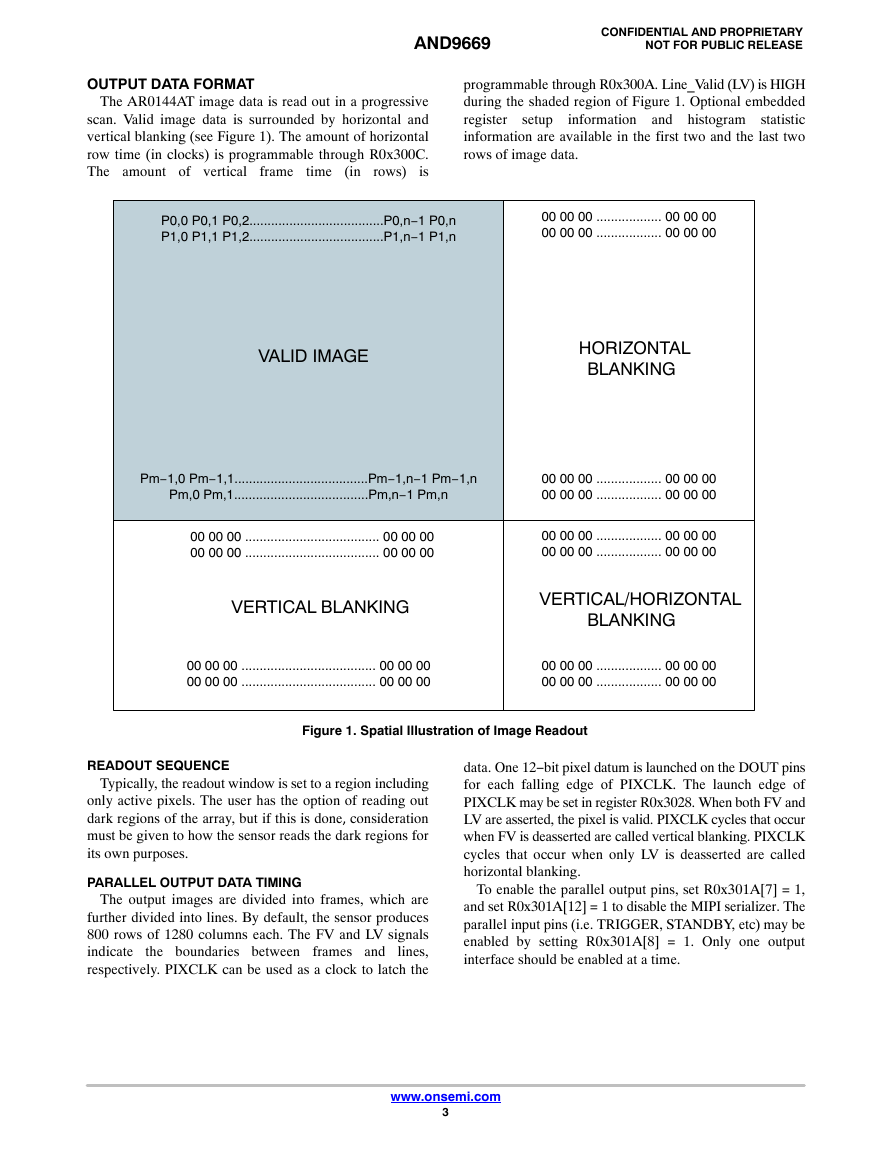
OUTPUT DATA FORMAT
The AR0144AT image data is read out in a progressive
scan. Valid image data is surrounded by horizontal and
vertical blanking (see Figure 1). The amount of horizontal
row time (in clocks) is programmable through R0x300C.
The amount of vertical frame
is
time (in rows)
programmable through R0x300A. Line_Valid (LV) is HIGH
during the shaded region of Figure 1. Optional embedded
register setup
information and histogram statistic
information are available in the first two and the last two
rows of image data.
P0,0 P0,1 P0,2.....................................P0,n−1 P0,n
P1,0 P1,1 P1,2.....................................P1,n−1 P1,n
00 00 00 .................. 00 00 00
00 00 00 .................. 00 00 00
VALID IMAGE
HORIZONTAL
BLANKING
Pm−1,0 Pm−1,1.....................................Pm−1,n−1 Pm−1,n
Pm,0 Pm,1.....................................Pm,n−1 Pm,n
00 00 00 .................. 00 00 00
00 00 00 .................. 00 00 00
00 00 00 ..................................... 00 00 00
00 00 00 ..................................... 00 00 00
00 00 00 .................. 00 00 00
00 00 00 .................. 00 00 00
VERTICAL BLANKING
VERTICAL/HORIZONTAL
BLANKING
00 00 00 ..................................... 00 00 00
00 00 00 ..................................... 00 00 00
00 00 00 .................. 00 00 00
00 00 00 .................. 00 00 00
Figure 1. Spatial Illustration of Image Readout
READOUT SEQUENCE
Typically, the readout window is set to a region including
only active pixels. The user has the option of reading out
dark regions of the array, but if this is done, consideration
must be given to how the sensor reads the dark regions for
its own purposes.
PARALLEL OUTPUT DATA TIMING
The output images are divided into frames, which are
further divided into lines. By default, the sensor produces
800 rows of 1280 columns each. The FV and LV signals
indicate
lines,
respectively. PIXCLK can be used as a clock to latch the
the boundaries between frames and
data. One 12−bit pixel datum is launched on the DOUT pins
for each falling edge of PIXCLK. The launch edge of
PIXCLK may be set in register R0x3028. When both FV and
LV are asserted, the pixel is valid. PIXCLK cycles that occur
when FV is deasserted are called vertical blanking. PIXCLK
cycles that occur when only LV is deasserted are called
horizontal blanking.
To enable the parallel output pins, set R0x301A[7] = 1,
and set R0x301A[12] = 1 to disable the MIPI serializer. The
parallel input pins (i.e. TRIGGER, STANDBY, etc) may be
enabled by setting R0x301A[8] = 1. Only one output
interface should be enabled at a time.
www.onsemi.com
3
�
CONFIDENTIAL AND PROPRIETARY
NOT FOR PUBLIC RELEASE
AND9669
PIXCLK
FV
LV
DOUT[11:0]
P0
P1
P2
P3
Pn
Vertical Blanking Horiz Blanking
Valid Image Data Horiz Blanking Vertical Blanking
Figure 2. Default Pixel Output Timing
LV and FV
The timing of the FV and LV outputs is closely related to
the row time and the frame time. FV will be asserted for an
integral number of row times, which will normally be equal
to the height of the output image.
LV will be asserted during the valid pixels of each row.
The leading edge of LV will be offset from the leading edge
of FV by 6 PIXCLKs. Normally, LV will only be asserted if
FV is asserted; this is configurable as described below.
LV Format Options
The default situation (R0x306E[1:0] = 0x0) is for LV to
be de−asserted when FV is de−asserted. By setting
R0x306E[1:0]= 0x1, a continuous LV signal will be output.
The formats for reading out three lines and two vertical
blanking lines are shown in Figure 3.
Default
Continuous LV
FV
LV
FV
LV
Figure 3. LV Format Options
The timing of an entire frame is shown below in Figure 4:
“Line Timing and FRAME_VALID/ LINE_VALID
Signals”. For detailed timing diagrams and switching
parameters, refer to the AR0144AT data sheet.
the maximum rate of one pixel per PIXCLK. One row time
(tROW) is the period from the first pixel output in a row to the
first pixel output in the next row. The row time and frame
time are defined by equations in Table 1.
Frame Time
The pixel clock (PIXCLK) represents the time needed to
sample one pixel from the array. The sensor outputs data at
FRAME_VALID
LINE_VALID
...
...
...
Number of master clocks
P1
A
Q
A
Q
A
P2
Figure 4. Line Timing and FRAME_VALID/LINE_VALID Signals
www.onsemi.com
4
�
AND9669
CONFIDENTIAL AND PROPRIETARY
NOT FOR PUBLIC RELEASE
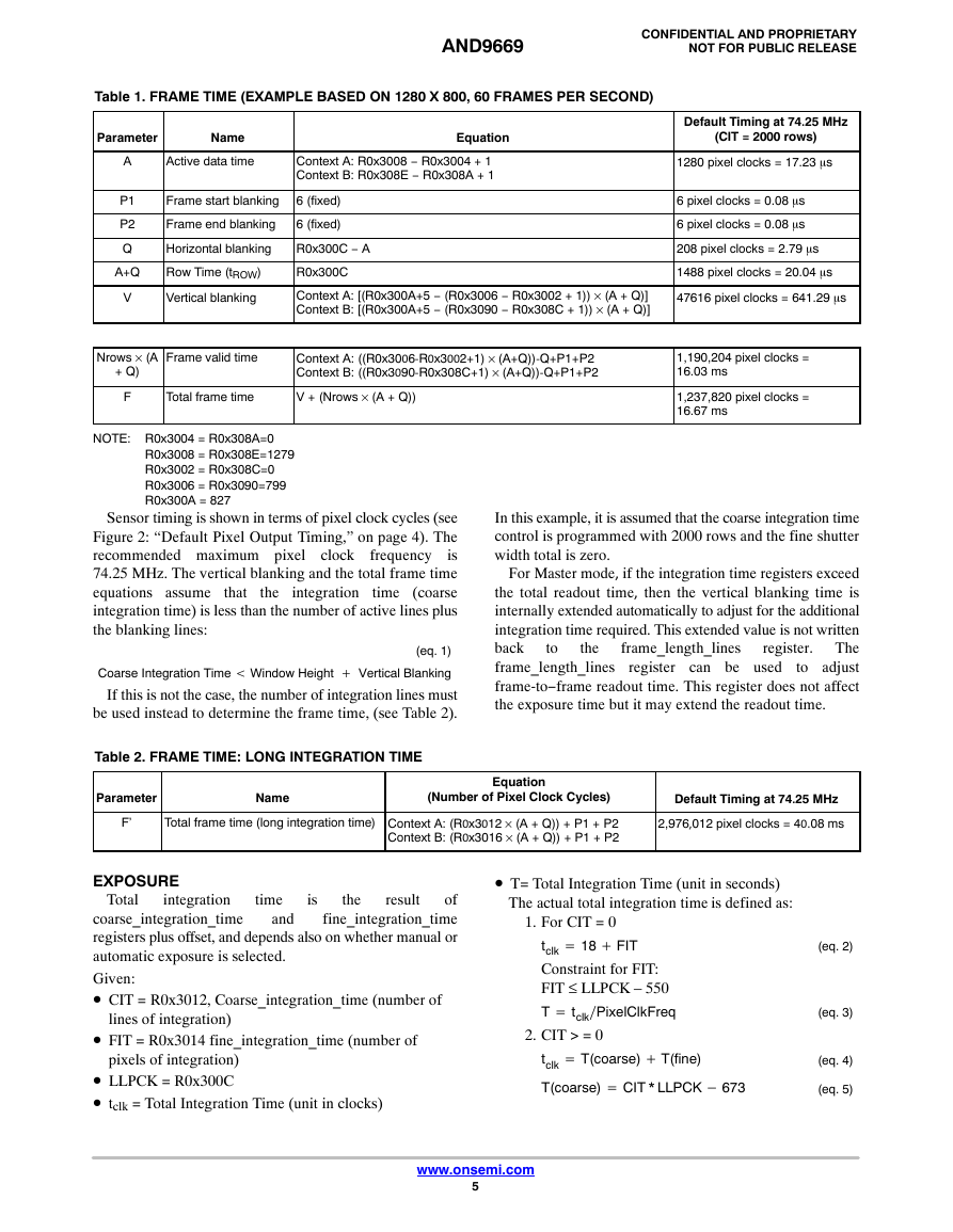
Table 1. FRAME TIME (EXAMPLE BASED ON 1280 X 800, 60 FRAMES PER SECOND)
Parameter
Name
Equation
A
P1
P2
Q
Active data time
Context A: R0x3008 − R0x3004 + 1
Context B: R0x308E − R0x308A + 1
Frame start blanking
6 (fixed)
Frame end blanking
6 (fixed)
Horizontal blanking
R0x300C − A
A+Q
Row Time (tROW)
V
Vertical blanking
R0x300C
Context A: [(R0x300A+5 − (R0x3006 − R0x3002 + 1)) × (A + Q)]
Context B: [(R0x300A+5 − (R0x3090 − R0x308C + 1)) × (A + Q)]
Nrows × (A
+ Q)
Frame valid time
F
Total frame time
Context A: ((R0x3006-R0x3002+1) × (A+Q))-Q+P1+P2
Context B: ((R0x3090-R0x308C+1) × (A+Q))-Q+P1+P2
V + (Nrows × (A + Q))
Default Timing at 74.25 MHz
(CIT = 2000 rows)
1280 pixel clocks = 17.23 ms
6 pixel clocks = 0.08 ms
6 pixel clocks = 0.08 ms
208 pixel clocks = 2.79 ms
1488 pixel clocks = 20.04 ms
47616 pixel clocks = 641.29 ms
1,190,204 pixel clocks =
16.03 ms
1,237,820 pixel clocks =
16.67 ms
NOTE: R0x3004 = R0x308A=0
R0x3008 = R0x308E=1279
R0x3002 = R0x308C=0
R0x3006 = R0x3090=799
R0x300A = 827
Sensor timing is shown in terms of pixel clock cycles (see
Figure 2: “Default Pixel Output Timing,” on page 4). The
recommended maximum pixel clock
is
74.25 MHz. The vertical blanking and the total frame time
equations assume
time (coarse
integration time) is less than the number of active lines plus
the blanking lines:
integration
frequency
that
the
(eq. 1)
Coarse Integration Time t Window Height ) Vertical Blanking
If this is not the case, the number of integration lines must
be used instead to determine the frame time, (see Table 2).
Table 2. FRAME TIME: LONG INTEGRATION TIME
In this example, it is assumed that the coarse integration time
control is programmed with 2000 rows and the fine shutter
width total is zero.
For Master mode, if the integration time registers exceed
the total readout time, then the vertical blanking time is
internally extended automatically to adjust for the additional
integration time required. This extended value is not written
register. The
back
frame_length_lines register can be used
to adjust
frame-to−frame readout time. This register does not affect
the exposure time but it may extend the readout time.
frame_length_lines
the
to
Parameter
F’
Name
(Number of Pixel Clock Cycles)
Total frame time (long integration time) Context A: (R0x3012 × (A + Q)) + P1 + P2
Context B: (R0x3016 × (A + Q)) + P1 + P2
Default Timing at 74.25 MHz
2,976,012 pixel clocks = 40.08 ms
Equation
EXPOSURE
is
the
and
time
Total
result
integration
of
coarse_integration_time
fine_integration_time
registers plus offset, and depends also on whether manual or
automatic exposure is selected.
Given:
• CIT = R0x3012, Coarse_integration_time (number of
• FIT = R0x3014 fine_integration_time (number of
pixels of integration)
• LLPCK = R0x300C
• tclk = Total Integration Time (unit in clocks)
lines of integration)
• T= Total Integration Time (unit in seconds)
The actual total integration time is defined as:
1. For CIT = 0
+ 18 ) FIT
tclk
Constraint for FIT:
FIT ≤ LLPCK – 550
ńPixelClkFreq
T + tclk
2. CIT > = 0
+ T(coarse) ) T(fine)
tclk
T(coarse) + CIT * LLPCK * 673
(eq. 2)
(eq. 3)
(eq. 4)
(eq. 5)
www.onsemi.com
5
�
CONFIDENTIAL AND PROPRIETARY
NOT FOR PUBLIC RELEASE
AND9669
Constraint for FIT:
FIT ≤ LLPCK – 740
T(fine) + FIT
T + tclk
ńPixelClkFreq
With the restrictions that:
(eq. 6)
(eq. 7)
1. When automatic exposure control (AEC) is
disabled:
a. The number of lines of integration for Context
A equals the value in R0x3012, and for Context B
equals the value in R0x3016.
b. The number of pixels of integration for Context
A equals the value in R0x3014, and for Context B
equals the value in R0x3018.
2. When automatic exposure control (AEC) is
enabled, the number of lines of integration may
vary from frame to frame, with the limits
controlled by R0x311E (minimum auto exposure
time) and R0x311C (maximum auto exposure
time). For a specific frame output, the exposure
time (in rows) can be read in R0x3164. Fine
integration time is not used by the auto exposure
function.
If the exposure time is to be set to approximately 2 ms and
default settings are being used (where one row−time equals
20 μs), a value of “100” is entered in R0x3012 (2 ms / 20 μs
= 100). In this mode, only whole number row−time
increments are allowed−no fractional time increments can
be achieved. It may be possible to adjust the number of
horizontal active or blanking pixels to bring the desired
exposure time to a whole number row−time increment.
The exposure time using the default power up settings of
the sensor can be determined as follows:
(eq. 8)
exposure_time + coarse_integration_time row_time
(eq. 9)
exposure_time + (100 rows) (20 ms) + 2 ms
Typically, the value of the coarse_integration_time
register is limited to the number of lines per frame (which
includes vertical blanking lines), such that the frame rate is
not affected by the integration time.
ROW−TIME DEFINITION
One row−time is equal to the sum of the number of active
pixels (columns) and the number of horizontal blanking
pixels divided by the pixel readout rate:
row_time + active_pixel ) horizontal_blank_pixels
(eq. 10)
PIXCLK_frequency
row_timedefault_settings
+ line_length_pck(R0x300C)
PIXCLK_frequency
(eq. 11)
+ line_length_pck(1488)
74.25 MHz
+ 20.04 ms
FRAME TIME DEFINITION
When frame_length_lines > coarse_integration_time:
rows_per_frame = frame_length_lines + overhead =
frame_length_lines + 5
When frame_length_lines <= coarse_integration_time:
rows_per_frame = coarse_integration_time − 2 + overhead
= coarse_integration_time + 3
Frame Time = rows_per_frame × row_time
EXPOSURE INDICATOR
The AR0144AT provides an output pin, FLASH, to
indicate when the exposure takes place. When R0x3270[8]
is set, FLASH is HIGH during exposure.
REAL−TIME CONTEXT SWITCHING
In the AR0144AT, the user may switch between two full
register sets (listed in Table 3) by writing to a context switch
change bit in R0x30B0[13]. This context switch will change
all registers (no shadowing) at the frame start time and have
the new values apply to the immediate next exposure and
readout time.
Table 3. REAL−TIME CONTEXT−SWITCHABLE REGISTERS
Register Number
Register Description
y_addr_start
x_addr_start
y_addr_end
x_addr_end
coarse_integration_time
fine_integration_time
x_odd_inc
y_odd_Inc
Context A
R0x3002
R0x3004
R0x3006
R0x3008
R0x3012
R0x3014
R0x30A2
R0x30A6
www.onsemi.com
6
Context B
R0x308C
R0x308A
R0x3090
R0x308E
R0x3016
R0x3018
R0x30AE
R0x30A8
�
AND9669
CONFIDENTIAL AND PROPRIETARY
NOT FOR PUBLIC RELEASE
Table 3. REAL−TIME CONTEXT−SWITCHABLE REGISTERS
Register Number
Register Description
Register Description
green1_gain (GreenR)
blue_gain
red_gain
green2_gain (GreenB)
global_gain
frame_length_lines
coarse_analog_gain
fine_analog_gain
col_bin
row_bin
line_length_pck
operation_mode
col_sf_bin_en
col_sf_bin_mono_en
Context A
R0x3056
R0x3058
R0x305A
R0x305C
R0x305E
R0x300A
R0x3060[6:4]
R0x3060[3:0]
R0x3040[13]
R0x3040[12]
R0x300C
R0x3082[1:0]
R0x3040[9]
R0x3040[7]
Context B
R0x30BC
R0x30BE
R0x30C0
R0x30C2
R0x30C4
R0x30AA
R0x3060[14:12]
R0x3060[11:8]
R0x3040[11]
R0x3040[10]
R0x303E
R0x3084[1:0]
R0x3040[8]
R0x3040[6]
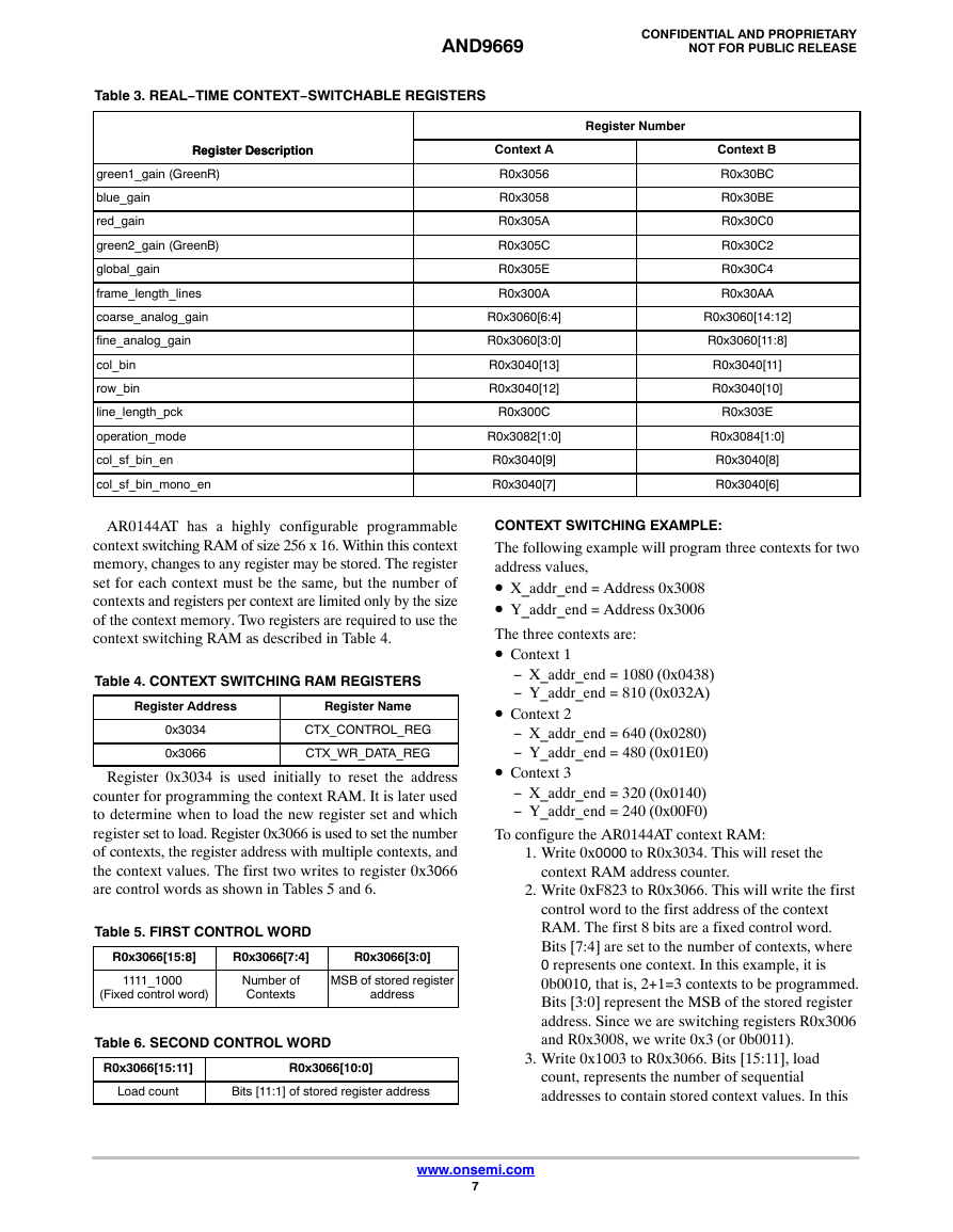
AR0144AT has a highly configurable programmable
context switching RAM of size 256 x 16. Within this context
memory, changes to any register may be stored. The register
set for each context must be the same, but the number of
contexts and registers per context are limited only by the size
of the context memory. Two registers are required to use the
context switching RAM as described in Table 4.
Table 4. CONTEXT SWITCHING RAM REGISTERS
Register Address
Register Name
0x3034
0x3066
CTX_CONTROL_REG
CTX_WR_DATA_REG
Register 0x3034 is used initially to reset the address
counter for programming the context RAM. It is later used
to determine when to load the new register set and which
register set to load. Register 0x3066 is used to set the number
of contexts, the register address with multiple contexts, and
the context values. The first two writes to register 0x3066
are control words as shown in Tables 5 and 6.
Table 5. FIRST CONTROL WORD
R0x3066[15:8]
R0x3066[7:4]
R0x3066[3:0]
1111_1000
(Fixed control word)
Number of
Contexts
MSB of stored register
address
Table 6. SECOND CONTROL WORD
R0x3066[15:11]
R0x3066[10:0]
Load count
Bits [11:1] of stored register address
CONTEXT SWITCHING EXAMPLE:
The following example will program three contexts for two
address values,
• X_addr_end = Address 0x3008
• Y_addr_end = Address 0x3006
The three contexts are:
• Context 1
− X_addr_end = 1080 (0x0438)
− Y_addr_end = 810 (0x032A)
• Context 2
− X_addr_end = 640 (0x0280)
− Y_addr_end = 480 (0x01E0)
• Context 3
− X_addr_end = 320 (0x0140)
− Y_addr_end = 240 (0x00F0)
To configure the AR0144AT context RAM:
1. Write 0x0000 to R0x3034. This will reset the
context RAM address counter.
2. Write 0xF823 to R0x3066. This will write the first
control word to the first address of the context
RAM. The first 8 bits are a fixed control word.
Bits [7:4] are set to the number of contexts, where
0 represents one context. In this example, it is
0b0010, that is, 2+1=3 contexts to be programmed.
Bits [3:0] represent the MSB of the stored register
address. Since we are switching registers R0x3006
and R0x3008, we write 0x3 (or 0b0011).
3. Write 0x1003 to R0x3066. Bits [15:11], load
count, represents the number of sequential
addresses to contain stored context values. In this
www.onsemi.com
7
�
CONFIDENTIAL AND PROPRIETARY
NOT FOR PUBLIC RELEASE
AND9669
example, it is 0b00010, that is, two consecutive
registers, R0x3006 and R0x3008 are to be
configured. Bits [10:0] represent bits [11:1] of the
address of the first register to be configured. Bit 0
is not needed because all address values are even.
In this case, we are writing bits [11:1] of R0x3006.
4. Program the register values for R0x3006
a. Write 0x032A to R0x3066
b. Write 0x01E0 to R0x3066
c. Write 0x00F0 to R0x3066
5. Program the register values for R0x3008
a. Write 0x0438 to R0x3066
b. Write 0x0280 to R0x3066
c. Write 0x0140 to R0x3066
6. The load counter has now expired, so a new
command is expected. This may be a new set of
context registers to be programmed. In this case,
return to step 2.
7. If all desired context registers have been
configured, write 0x0000 to R0x3066 to end the
programming sequence.
If the desired context switchable registers do not share the
same MSB in address, the programming procedure will need
to skip back to step 2 to load the new MSB in R0x3066[3:0].
SWITCHING CONTEXTS
Once the context RAM has been configured, register
R0x3034 is then used to determine when to switch contexts,
and to which context to switch. Table 7 describes how to
control context switching.
Table 7. CONTEXT SWITCH CONTROL
CTX_CONTROL_REG
Description
R0x3034[15] = 0x1
Load the new context immediately
R0x3034[3:0]
Determines which context to load
FEATURES
NOTE: See the AR0144AT Register Reference for
additional details.
OPERATIONAL MODES
Master Mode
The AR0144AT works in master (video) or trigger (single
frame) modes. In master mode, the sensor generates the
integration and readout timing. In trigger mode, it accepts an
external trigger to start exposure, then generates the
exposure and readout timing. The exposure time is
programmed through the two−wire serial interface for both
modes.
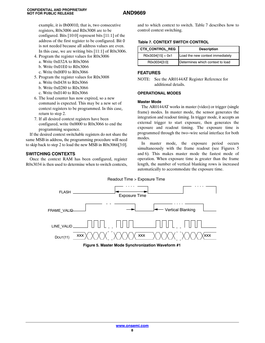
In master mode,
the exposure period occurs
simultaneously with the frame readout (see Figures 5
and 6). This makes master mode the fastest mode of
operation. When exposure time is greater than the frame
length, the number of vertical blanking rows is increased
automatically to accommodate the exposure time.
FLASH
FRAME_VALID
LINE_VALID
DOUT(11)
xxx
Readout Time > Exposure Time
Exposure Time
Vertical Blanking
xxx
xxx
Figure 5. Master Mode Synchronization Waveform #1
www.onsemi.com
8
�






 2023年江西萍乡中考道德与法治真题及答案.doc
 2012年重庆南川中考生物真题及答案.doc
 2013年江西师范大学地理学综合及文艺理论基础考研真题.doc
 2020年四川甘孜小升初语文真题及答案I卷.doc
 2020年注册岩土工程师专业基础考试真题及答案.doc
 2023-2024学年福建省厦门市九年级上学期数学月考试题及答案.doc
 2021-2022学年辽宁省沈阳市大东区九年级上学期语文期末试题及答案.doc
 2022-2023学年北京东城区初三第一学期物理期末试卷及答案.doc
 2018上半年江西教师资格初中地理学科知识与教学能力真题及答案.doc
 2012年河北国家公务员申论考试真题及答案-省级.doc
 2020-2021学年江苏省扬州市江都区邵樊片九年级上学期数学第一次质量检测试题及答案.doc
 2022下半年黑龙江教师资格证中学综合素质真题及答案.doc