AR0144AT
Advance Information
1/4‐inch 1.0 Mp CMOS
Digital Image Sensor
with Global Shutter
Description
The AR0144AT is a 1/4-inch 1.0 Mp CMOS digital image sensor
with an active-pixel array of 1280 (H) × 800 (V). It incorporates a new
innovative global shutter pixel design optimized for accurate and fast
capture of moving scenes. The sensor produces clear, low noise
images in both low-light and bright scenes. It includes sophisticated
camera functions such as auto exposure control, windowing, row skip
mode, column-skip mode, pixel-binning and both video and single
frame modes. It is programmable through a simple two-wire serial
interface. The AR0144AT produces extraordinarily clear, sharp digital
pictures, and its ability to capture both continuous video and single
frames makes it the perfect choice for a wide range of applications,
including automotive in-cabin systems.
Table 1. KEY PERFORMANCE PARAMETERS
Parameter
Typical Value
Optical Format
Active Pixels
Pixel Size
Color Filter Array
Chief Ray Angle
Shutter Type
Input Clock Range
Output Pixel Clock (Maximum)
Output
Serial
Parallel
Frame Rate
Full Resolution
720p
Responsivity
Monochrome
Color
SNRMAX
Dynamic Range
Supply Voltage
I/O
Digital
Analog
Power Consumption
Operating Temperature
Package Options
1/4-inch (4.5 mm)
1280 (H) × 800 (V) = 1.0 Mp
3.0 mm
RGB Bayer or Monochrome
20°
Global Shutter
6–64 MHz
74.25 MHz
MIPI, 2-lane
12-bit
60 fps
66 fps
3.6 V/lux−sec
3.1 V/lux−sec
38 dB
63.9 dB
1.8 or 2.8 V
1.2 V
2.8 V
< 250 mW
–40°C to + 105°C (Ambient)
–40°C to + 125°C (Junction)
7 × 7 mm 63-ball iBGA
Bare Die
This document contains information on a new product. Specifications and information
herein are subject to change without notice.
www.onsemi.com
IBGA63 7 y 7
CASE TBD
ORDERING INFORMATION
See detailed ordering and shipping information on page 2 of
this data sheet.
Windowing and Pixel Binning
Features
• Superior Low-light and IR Performance
• HD Video (720p60)
• 2-lane MIPI or Parallel Data Interface
• Automatic Black Level Calibration (ABLC)
• Programmable Control for Region Of
• Horizontal and Vertical Mirroring,
• On-chip Auto Exposure Control for Any
• 5 × 5 Statistics Engine for Any
• Flexible Control for Row and Column Skip
• On-chip Slave or Trigger Mode for
• Built in Strobe Control
• On Chip Phase Lock Loop (PLL)
• On-chip Slave or Trigger Mode for
Programmable ROI
Programmable ROI
Interest (ROI)
Mode
Synchronization
Synchronization
Applications
• In Cabin Automotive
♦ Gesture Recognition
♦ Iris Scanning
♦ Head Roll
♦ Eye Tracking
♦ Augmented Reality
♦ Machine Vision
• Others Such as Barcode Scanner, Biometric
© Semiconductor Components Industries, LLC, 2016
December, 2016 − Rev. P0
1
Publication Order Number:
AR0144AT/D
�
AR0144AT
ORDERING INFORMATION
Table 2. AVAILABLE PART NUMBERS
Part Number
AR0144ATSM20XUEA0−DRBR−E
AR0144ATSC20XUEA0−DRBR−E
AR0144ATSM20XUEA0−DRBR
AR0144ATSC20XUEA0−DRBR
AR0144ATSM20XUEA0−GEVB
AR0144ATSC20XUEA0−GEVB
Product Description
Mono, iBGA
RGB, iBGA
Mono, iBGA
RGB, iBGA
Mono, iBGA, Headboard Mono, Headboard
RGB, iBGA, Headboard
RGB, Headboard
Orderable Product Attribute Description
Mono, iBGA, CRA = 20°, without PF, Double Sided BBAR Glass, Samples
RGB, iBGA, CRA = 20°, without PF, Double Sided BBAR Glass, Samples
Mono, iBGA, CRA = 20°, without PF, Double Sided BBAR Glass
RGB, iBGA, CRA = 20°, without PF, Double Sided BBAR Glass
See the ON Semiconductor Device Nomenclature
document (TND310/D) for a full description of the naming
convention used for
image sensors. For reference
documentation, including information on evaluation kits,
please visit our web site at www.onsemi.com.
GENERAL DESCRIPTION
The ON Semiconductor AR0144AT can be operated in its
default mode or programmed for frame size, exposure, gain,
and other parameters. The default mode output is
a full-resolution image at 60 frames per second (fps). It
outputs 12-bit raw data, using either the parallel or serial
(MIPI) output ports. The device may be operated in video
(master) mode or in frame trigger mode.
FRAME_VALID and LINE_VALID signals are output on
dedicated pins, along with a synchronized pixel clock.
A dedicated FLASH pin can be programmed to control
external LED or flash exposure illumination.
The AR0144AT includes additional features to allow
application-specific
adjustable
auto-exposure control, auto black level correction, on-board
temperature sensor, row-skip and column-skip modes and
binning modes.
tuning: windowing,
The sensor is designed to operate in a wide temperature
range (–40°C to +105°C).
FUNCTIONAL OVERVIEW
The AR0144AT is a progressive-scan sensor that
generates a stream of pixel data at a constant frame rate. It
uses an on-chip, phase-locked loop (PLL) that can be
optionally enabled to generate all internal clocks from
a single master input clock running between 6 and 64 MHz.
The maximum output pixel
is 74.25 Mp/s,
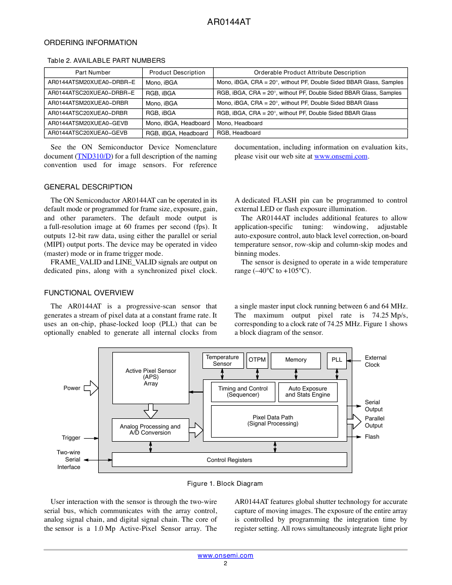
corresponding to a clock rate of 74.25 MHz. Figure 1 shows
a block diagram of the sensor.
rate
Power
Trigger
Two-wire
Serial
Interface
Active Pixel Sensor
(APS)
Array
Analog Processing and
A/D Conversion
Temperature
Sensor
OTPM
Memory
PLL
Timing and Control
(Sequencer)
Auto Exposure
and Stats Engine
Pixel Data Path
(Signal Processing)
External
Clock
Serial
Output
Parallel
Output
Flash
Control Registers
Figure 1. Block Diagram
User interaction with the sensor is through the two-wire
serial bus, which communicates with the array control,
analog signal chain, and digital signal chain. The core of
the sensor is a 1.0 Mp Active-Pixel Sensor array. The
AR0144AT features global shutter technology for accurate
capture of moving images. The exposure of the entire array
is controlled by programming the integration time by
register setting. All rows simultaneously integrate light prior
www.onsemi.com
2
�
AR0144AT
to readout. Once a row has been read, the data from the
columns is sequenced through an analog signal chain
(providing offset correction and gain), and then through an
analog-to-digital converter (ADC). The output from the
ADC is a 12-bit value for each pixel in the array. The ADC
output passes through a digital processing signal chain
(which provides further data path corrections and applies
digital gain). The pixel data are output at a rate of up to
74.25 Mp/s, in parallel to frame and line synchronization
signals.
FEATURES OVERVIEW
The AR0144AT Global Shutter sensor has a wide array of
features to enhance functionality and to increase versatility.
A summary of features follows. Please refer to the AR0144
Developer Guide for detailed feature descriptions, register
settings, and tuning guidelines and recommendations.
• 3.0 mm Global Shutter Pixel
To improve the low light performance and to capture
the moving images accurately a large (3.0 mm) global
shutter pixel is implemented for better image
optimization.
• Operating Modes
The AR0144AT works in master (video), trigger (single
frame), or Auto Trigger modes. In master mode,
the sensor generates the integration and readout timing.
In trigger mode, it accepts an external trigger to start
exposure, then generates the exposure and readout
timing. The exposure time is programmed through the
two-wire serial interface for both modes.
• Window Control
Configurable window size and blanking times allow
a wide range of resolutions and frame rates. Digital
binning and skipping modes are supported, as are
vertical and horizontal mirror operations.
• Frame Rate
AR0144AT is capable of running up to 60 fps at full
(1280 × 800) resolution and 66 fps at 720p resolution.
• Embedded Data and Statistics
The AR0144AT has the capability to output image data
and statistics embedded within the frame timing.
• Multi-Camera Synchronization
The AR0144AT supports advanced line synchronization
controls for multi-camera (stereo) support.
• Slave Mode
The slave mode feature of the AR0144AT supports
triggering the start of a frame readout from an input
signal that is supplied from an external source.
The slave mode signal allows for precise control of
frame rate and register change updates.
• Context Switching and Register Updates
Context switching may be used to rapidly switch
between two sets of register values.
Refer to the AR0144 Developer Guide for a complete
description of context switchable registers.
• Gain
A programmable analog gain of 1x to 16x applied
globally to all color channels is available along with
a digital gain of 1x to 16x that may be configured on
a per color channel basis.
• Automatic Exposure Control
The integrated automatic exposure control may be used
to ensure optimal settings of exposure and gain are
computed and updated every other frame. Refer to the
AR0144 Developer Guide for more details.
• MIPI
The AR0144AT Global Shutter image sensor supports
two lanes of MIPI data. Compliant to MIPI standards:
♦ MIPI Alliance Standard for CSI−2 version 1.2
♦ MIPI Alliance Standard for D−PHY version 1.0
• PLL
An on chip PLL provides reference clock flexibility and
supports spread spectrum sources for improved EMI
performance.
• Reset
The AR0144AT may be reset by a register write, or by
a dedicated input pin.
• Output Enable
The AR0144AT output pins may be tri-stated using
a dedicated output enable pin.
• Temperature Sensor
• Black Level Correction
• Row Noise Correction
• Test Patterns
Several test patterns may be enabled for debug
purposes. These include a solid color, color bar, fade to
gray, and a walking 1s test pattern.
• Silicon/OTPM Revision Information
A revision register is provided to read out (via I2C)
silicon and OTPM revision information. This will be
helpful to distinguish material if there are future OTPM
or silicon revisions.
• Lens Shading Correction
A lens shading correction algorithm is included for
potential low Z height applications.
• Compression
AR0144AT can optionally compress 12-bit data to
10-bit using A-law compression.
www.onsemi.com
3
�
AR0144AT
PIXEL DATA FORMAT
Pixel Array Structure
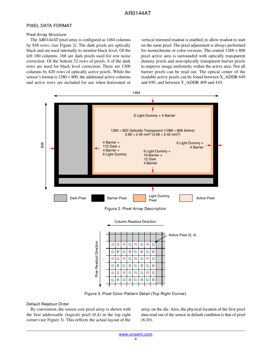
The AR0144AT pixel array is configured as 1484 columns
by 856 rows, (see Figure 2). The dark pixels are optically
black and are used internally to monitor black level. Of the
left 180 columns, 168 are dark pixels used for row noise
correction. Of the bottom 32 rows of pixels, 8 of the dark
rows are used for black level correction. There are 1300
columns by 820 rows of optically active pixels. While the
sensor’s format is 1280 × 800, the additional active columns
and active rows are included for use when horizontal or
vertical mirrored readout is enabled, to allow readout to start
on the same pixel. The pixel adjustment is always performed
for monochrome or color versions. The central 1288 × 808
pixel active area is surrounded with optically transparent
dummy pixels and non-optically transparent barrier pixels
to improve image uniformity within the active area. Not all
barrier pixels can be read out. The optical center of the
readable active pixels can be found between X_ADDR 649
and 650, and between Y_ADDR 409 and 410.
1484
6 Light Dummy + 4 Barrier
6
5
8
1300 × 820 Optically Transparent (1288 × 808 Active)
3.89 × 2.45 mm2 (3.86 × 2.42 mm2)
4 Barrier +
172 Dark +
4 Barrier +
6 Light Dummy
6 Light Dummy +
4 Barrier
6 Light Dummy +
16 Barrier +
12 Dark
4 Barrier
Dark Pixel
Barrier Pixel
Light Dummy
Pixel
Active Pixel
Figure 2. Pixel Array Description
Active Pixel (0, 4)
Column Readout Direction
…
G
B
G
B
G
B
R
G
R
G
R
G
G
B
G
B
G
B
R
G
R
G
R
G
G
B
G
B
G
B
…
R
G
R
G
R
G
G
B
G
B
G
B
R
G
R
G
R
G
n
o
i
t
c
e
r
i
D
t
u
o
d
a
e
R
w
o
R
Figure 3. Pixel Color Pattern Detail (Top Right Corner)
Default Readout Order
By convention, the sensor core pixel array is shown with
the first addressable (logical) pixel (0,4) in the top right
corner (see Figure 3). This reflects the actual layout of the
array on the die. Also, the physical location of the first pixel
data read out of the sensor in default condition is that of pixel
(6,10).
www.onsemi.com
4
�
AR0144AT
CONFIGURATION AND PINOUT
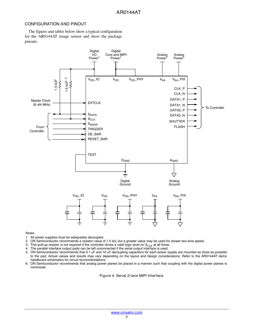
The figures and tables below show a typical configuration
for the AR0144AT image sensor and show the package
pinouts.
Digital
I/O
Power1
Digital
Core and MIPI
Power1
Analog
Power1
Analog
Power1
2
W
k
5
.
1
3
,
2
W
k
5
.
1
Master Clock
(6−64 MHz)
From
Controller
VDD_IO
VDD
VDD_PHY
VAA
VAA_PIX
CLK_P
CLK_N
DATA1_P
DATA1_N
DATA2_P
DATA2_N
SHUTTER
FLASH
To Controller
EXTCLK
SDATA
SCLK
SADDR
TRIGGER
OE_BAR
RESET_BAR
TEST
DGND
AGND
Digital
Ground
Analog
Ground
VDD_IO
VDD
VDD_PHY
VAA
VAA_PIX
Notes:
1. All power supplies must be adequately decoupled.
2. ON Semiconductor recommends a resistor value of 1.5 kW, but a greater value may be used for slower two-wire speed.
3. This pull-up resistor is not required if the controller drives a valid logic level on SCLK at all times.
4. The parallel interface output pads can be left unconnected if the serial output interface is used.
5. ON Semiconductor recommends that 0.1 mF and 10 mF decoupling capacitors for each power supply are mounted as close as possible
to the pad. Actual values and results may vary depending on the layout and design considerations. Refer to the AR0144AT demo
headboard schematics for circuit recommendations.
6. ON Semiconductor recommends that analog power planes be placed in a manner such that coupling with the digital power planes is
minimized.
Figure 4. Serial 2-lane MIPI Interface
www.onsemi.com
5
�
AR0144AT
Digital
Core
Power1
Analog
Power1
Analog
Power1
Digital
I/O
Power1
2
W
k
5
.
1
3
,
2
W
k
5
.
1
Master Clock
(6−64 MHz)
From
Controller
VDD_IO
VDD
VAA
VAA_PIX
EXTCLK
SDATA
SCLK
SADDR
TRIGGER
OE_BAR
RESET_BAR
TEST
DOUT[11:0]
PIXCLK
LINE_VALID
FRAME_VALID
SHUTTER
FLASH
To Controller
DGND
AGND
Digital
Ground
Analog
Ground
VDD_IO
VDD
VAA
VAA_PIX
Notes:
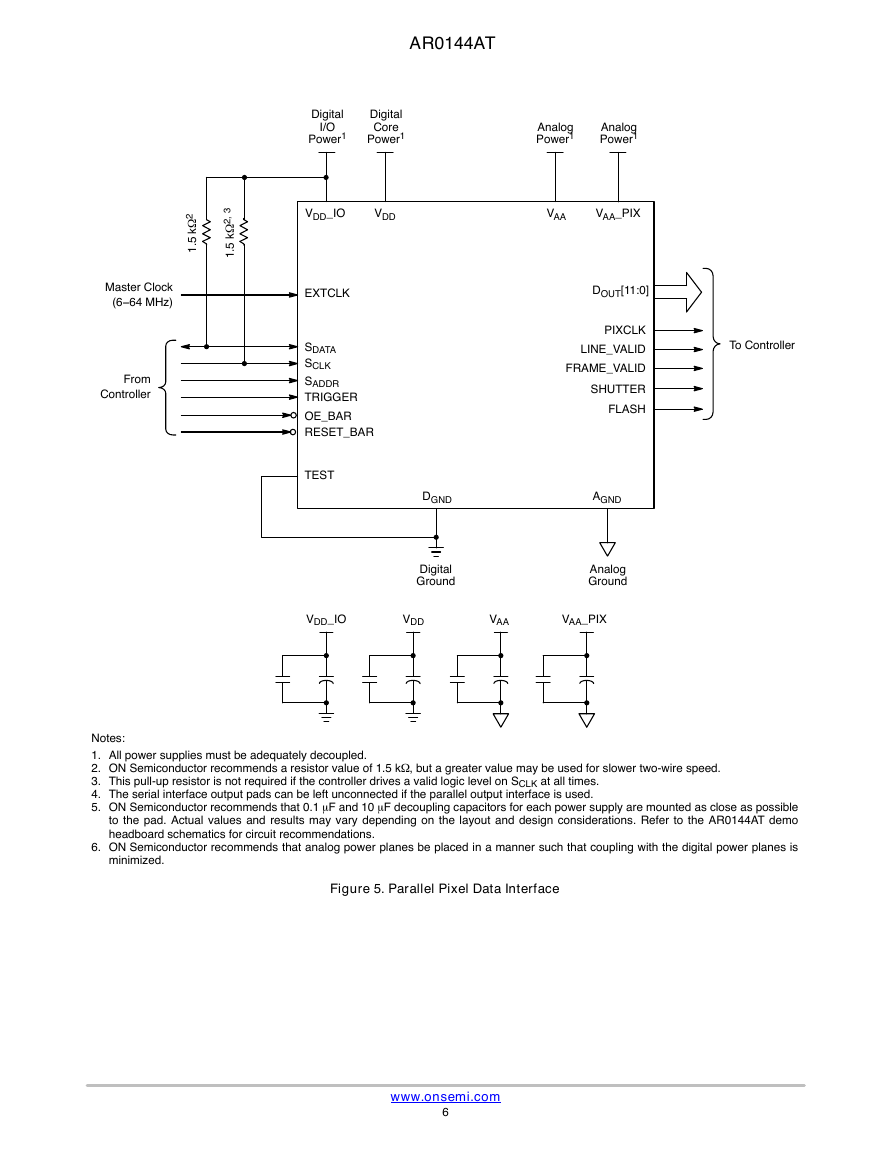
1. All power supplies must be adequately decoupled.
2. ON Semiconductor recommends a resistor value of 1.5 kW, but a greater value may be used for slower two-wire speed.
3. This pull-up resistor is not required if the controller drives a valid logic level on SCLK at all times.
4. The serial interface output pads can be left unconnected if the parallel output interface is used.
5. ON Semiconductor recommends that 0.1 mF and 10 mF decoupling capacitors for each power supply are mounted as close as possible
to the pad. Actual values and results may vary depending on the layout and design considerations. Refer to the AR0144AT demo
headboard schematics for circuit recommendations.
6. ON Semiconductor recommends that analog power planes be placed in a manner such that coupling with the digital power planes is
minimized.
Figure 5. Parallel Pixel Data Interface
www.onsemi.com
6
�
AR0144AT
1
2
3
4
5
6
7
8
A
VDD
DGND
DATA1_N
CLK_N
DATA0_N
VDD
DGND
B
VDD_IO
DGND
EXTCLK
DATA1_P
CLK_P
DATA0_P
DGND
VDD_IO
C
DGND
LINE_
VALID
FRAME_
VALID
DGND
VDD_PHY
FLASH
SCLK
VDD
D
VDD_IO
DOUT10
DOUT11
PIXCLK
SHUTTER
SDATA
OE_BAR
AGND
E
F
DGND
DOUT6
DOUT7
DOUT8
DOUT9
TEST
DGND
Reserved
VDD
DOUT2
DOUT3
DOUT4
DOUT5
SADDR
TRIGGER
VAA_PIX
G
VAA
DGND
DOUT1
DOUT0
RESET_
BAR
Reserved
DGND
VAA
H
DGND
VDD
VAA
AGND
AGND
VAA
VDD
DGND
Top View
(Ball Down)
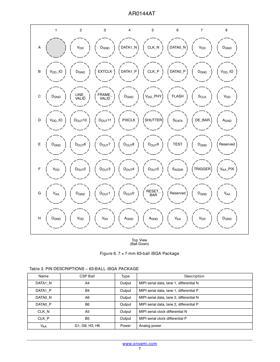
Figure 6. 7 y 7 mm 63-ball iBGA Package
Table 3. PIN DESCRIPTIONS − 63-BALL iBGA PACKAGE
Name
DATA1_N
DATA1_P
DATA0_N
DATA0_P
CLK_N
CLK_P
VAA
CSP Ball
Type
Description
A4
B4
A6
B6
A5
B5
G1, G8, H3, H6
Output
MIPI serial data, lane 1, differential N
Output
Output
Output
Output
Output
Power
MIPI serial data, lane 1, differential P
MIPI serial data, lane 2, differential N
MIPI serial data, lane 2, differential P
MIPI serial clock differential N
MIPI serial clock differential P
Analog power
www.onsemi.com
7
�
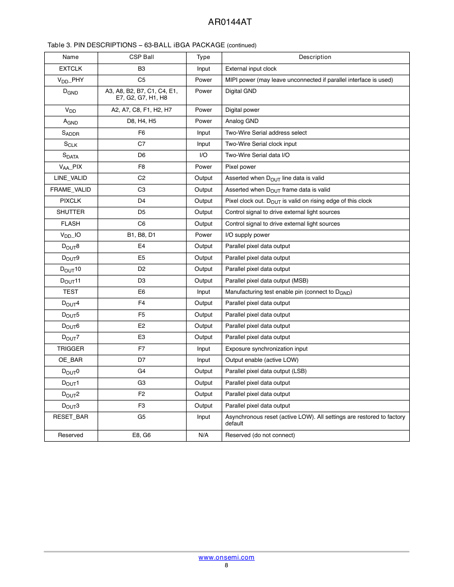
Table 3. PIN DESCRIPTIONS − 63-BALL iBGA PACKAGE (continued)
AR0144AT
Name
EXTCLK
VDD_PHY
DGND
VDD
AGND
SADDR
SCLK
SDATA
VAA_PIX
LINE_VALID
FRAME_VALID
PIXCLK
SHUTTER
FLASH
VDD_IO
DOUT8
DOUT9
DOUT10
DOUT11
TEST
DOUT4
DOUT5
DOUT6
DOUT7
TRIGGER
OE_BAR
DOUT0
DOUT1
DOUT2
DOUT3
RESET_BAR
CSP Ball
B3
C5
A3, A8, B2, B7, C1, C4, E1,
E7, G2, G7, H1, H8
A2, A7, C8, F1, H2, H7
D8, H4, H5
F6
C7
D6
F8
C2
C3
D4
D5
C6
B1, B8, D1
E4
E5
D2
D3
E6
F4
F5
E2
E3
F7
D7
G4
G3
F2
F3
G5
Type
Input
Power
Power
Power
Power
Input
Input
I/O
Power
Output
Output
Output
Output
Output
Power
Output
Output
Output
Output
Input
Output
Output
Output
Output
Input
Input
Output
Output
Output
Output
Input
External input clock
Description
MIPI power (may leave unconnected if parallel interface is used)
Digital GND
Digital power
Analog GND
Two-Wire Serial address select
Two-Wire Serial clock input
Two-Wire Serial data I/O
Pixel power
Asserted when DOUT line data is valid
Asserted when DOUT frame data is valid
Pixel clock out. DOUT is valid on rising edge of this clock
Control signal to drive external light sources
Control signal to drive external light sources
I/O supply power
Parallel pixel data output
Parallel pixel data output
Parallel pixel data output
Parallel pixel data output (MSB)
Manufacturing test enable pin (connect to DGND)
Parallel pixel data output
Parallel pixel data output
Parallel pixel data output
Parallel pixel data output
Exposure synchronization input
Output enable (active LOW)
Parallel pixel data output (LSB)
Parallel pixel data output
Parallel pixel data output
Parallel pixel data output
Asynchronous reset (active LOW). All settings are restored to factory
default
Reserved
E8, G6
N/A
Reserved (do not connect)
www.onsemi.com
8
�



 2023年江西萍乡中考道德与法治真题及答案.doc
 2012年重庆南川中考生物真题及答案.doc
 2013年江西师范大学地理学综合及文艺理论基础考研真题.doc
 2020年四川甘孜小升初语文真题及答案I卷.doc
 2020年注册岩土工程师专业基础考试真题及答案.doc
 2023-2024学年福建省厦门市九年级上学期数学月考试题及答案.doc
 2021-2022学年辽宁省沈阳市大东区九年级上学期语文期末试题及答案.doc
 2022-2023学年北京东城区初三第一学期物理期末试卷及答案.doc
 2018上半年江西教师资格初中地理学科知识与教学能力真题及答案.doc
 2012年河北国家公务员申论考试真题及答案-省级.doc
 2020-2021学年江苏省扬州市江都区邵樊片九年级上学期数学第一次质量检测试题及答案.doc
 2022下半年黑龙江教师资格证中学综合素质真题及答案.doc