UCC27323, UCC27324, UCC27325
UCC37323, UCC37324, UCC37325
SLUS492F − JUNE 2001 − REVISED MARCH 2009
DUAL 4ĆA PEAK HIGH SPEED LOW-SIDE POWER MOSFET DRIVERS
FEATURES
D Industry-Standard Pin-Out
D High Current Drive Capability of ±4 A at the
Miller Plateau Region
D Efficient Constant Current Sourcing Even at
Low Supply Voltages
D TTL/CMOS Compatible Inputs Independent
of Supply Voltage
D 20-ns Typical Rise and 15-ns Typical Fall
Times with 1.8-nF Load
D Typical Propagation Delay Times of 25 ns
with Input Falling and 35 ns with Input Rising
D 4-V to 15-V Supply Voltage
D Supply Current of 0.3 mA
D Dual Outputs Can Be Paralleled for Higher
Drive Current
D Available in Thermally Enhanced MSOP
PowerPADTM Package with 4.7°C/W θjc
D Rated From –40°C to 125°C
D TrueDrive Output Architecture Using Bipolar
and CMOS Transistors in Parallel
BLOCK DIAGRAM
APPLICATIONS
D Switch Mode Power Supplies
D DC/DC Converters
D Motor Controllers
D Line Drivers
D Class D Switching Amplifiers
DESCRIPTION
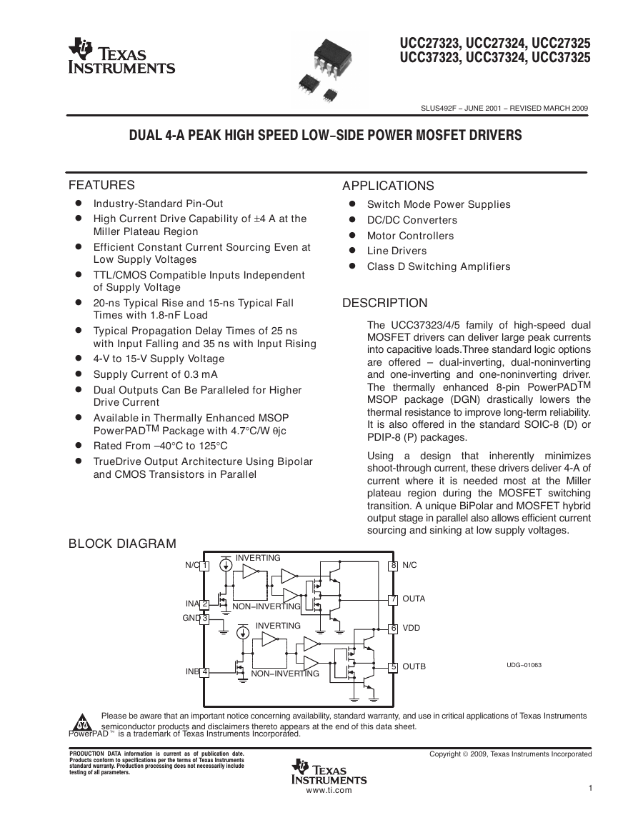
The UCC37323/4/5 family of high-speed dual
MOSFET drivers can deliver large peak currents
into capacitive loads.Three standard logic options
are offered – dual-inverting, dual-noninverting
and one-inverting and one-noninverting driver.
The thermally enhanced 8-pin PowerPADTM
MSOP package (DGN) drastically lowers the
thermal resistance to improve long-term reliability.
It is also offered in the standard SOIC-8 (D) or
PDIP-8 (P) packages.
that
Using a design
inherently minimizes
shoot-through current, these drivers deliver 4-A of
current where it is needed most at the Miller
plateau region during the MOSFET switching
transition. A unique BiPolar and MOSFET hybrid
output stage in parallel also allows efficient current
sourcing and sinking at low supply voltages.
N/C
1
INA
2
GND
3
INVERTING
NON−INVERTING
INVERTING
8
N/C
7
OUTA
6 VDD
INB
4
NON−INVERTING
5
OUTB
UDG−01063
Please be aware that an important notice concerning availability, standard warranty, and use in critical applications of Texas Instruments
semiconductor products and disclaimers thereto appears at the end of this data sheet.
PowerPADt is a trademark of Texas Instruments Incorporated.
information
PRODUCTION DATA
is current as of publication date.
Products conform to specifications per the terms of Texas Instruments
standard warranty. Production processing does not necessarily include
testing of all parameters.
Copyright 2009, Texas Instruments Incorporated
www.ti.com
1
�
UCC27323, UCC27324, UCC27325
UCC37323, UCC37324, UCC37325
SLUS492F − JUNE 2001 − REVISED MARCH 2009
ORDERING INFORMATION
OUTPUT
OUTPUT
CONFIGURATION
TEMPERATURE RANGE
TEMPERATURE RANGE
TA = TJ
Dual inverting
Dual inverting
Dual nonInverting
Dual nonInverting
One inverting,
One inverting,
one noninverting
−40°C to +125°C
0°C to +70°C
−40°C to +125°C
0°C to +70°C
−40°C to +125°C
0°C to +70°C
SOIC-8 (D)
UCC27323D
UCC37323D
UCC27324D
UCC37324D
UCC27325D
UCC37325D
PACKAGED DEVICES
MSOP-8 PowerPAD
(DGN)}
UCC27323DGN
UCC37323DGN
UCC27324DGN
UCC37324DGN
UCC27325DGN
UCC37325DGN
PDIP-8 (P)
UCC27323P
UCC37323P
UCC27324P
UCC37324P
UCC27325P
UCC37325P
† D (SOIC−8) and DGN (PowerPAD−MSOP) packages are available taped and reeled. Add R suffix to device type (e.g. UCC27323DR,
UCC27324DGNR) to order quantities of 2,500 devices per reel for D or 1,000 devices per reel for DGN package.
‡ The PowerPAD is not directly connected to any leads of the package. However, it is electrically and thermally connected to the substrate which
is the ground of the device.
D, DGN, OR P PACKAGE
(TOP VIEW)
D, DGN, OR P PACKAGE
(TOP VIEW)
D, DGN, OR P PACKAGE
(TOP VIEW)
N/A
1
INA
2
GND
3
INB
4
8
7
6
5
N/A
OUTA
VDD
OUTB
N/A
1
INA
2
GND
3
INB
4
8
7
6
5
N/A
OUTA
VDD
OUTB
N/A
1
INA
2
GND
3
INB
4
8
7
6
5
N/A
OUTA
VDD
OUTB
(DUAL INVERTING)
(DUAL NONINVERTING)
(ONE INVERTING,
ONE NONINVERTING)
power dissipation rating table
PACKAGE
SUFFIX
Θjc (°C/W)
Θja (°C/W)
Power Rating (mW)
TA = 70°C See Note 1
Derating Factor Above
70°C (mW/5C) See
Note 1
SOIC-8
PDIP-8
MSOP PowerPAD-8
See Note 3
D
P
DGN
42
49
4.7
84 – 160}
344−655 See Note 2
6.25 − 11.9 See Note 2
110
50 − 59}
500
1370
9
17.1
Notes: 1. 125°C operating junction temperature is used for power rating calculations
2. The range of values indicates the effect of pc−board. These values are intended to give the system designer an indication of the
best and worst case conditions. In general, the system designer should attempt to use larger traces on the pc−board where possible
in order to spread the heat away form the device more effectively. For information on the PowerPADt package, refer to Technical
Brief, PowerPad Thermally Enhanced Package, Texas Instrument s Literature No. SLMA002 and Application Brief, PowerPad Made
Easy, Texas Instruments Literature No. SLMA004.
3. The PowerPAD is not directly connected to any leads of the package. However, it is electrically and thermally connected to the
substrate which is the ground of the device.
Table 1. Input/Output Table
INPUTS (VIN_L, VIN_H)
UCC37323
UCC37324
UCC37325
INA
L
L
H
H
INB
L
H
L
H
OUTA OUTB OUTA OUTB OUTA OUTB
H
H
L
L
H
L
H
L
L
L
H
H
L
H
L
H
H
H
L
L
L
H
L
H
2
www.ti.com
�
absolute maximum ratings over operating free-air temperature (unless otherwise noted)†}
UCC27323, UCC27324, UCC27325
UCC37323, UCC37324, UCC37325
SLUS492F − JUNE 2001 − REVISED MARCH 2009
. . . . . . . . . . . . . . . . . . . . . . . . . . . . . . . . . . . . . . . . . . . . . . . . . . . . . . . . . . . . . . .
Supply voltage, VDD
Analog input (IN), and output voltage (OUTA, OUTB)
Output current (OUTA, OUTB) DC, IOUT_DC
Pulsed, (0.5 µs), IOUT_PULSED
Power dissipation at TA = 25°C (DGN package)
(D package)
(P package)
Junction operating temperature, TJ
Storage temperature, Tstg
Lead temperature (soldering, 10 sec.),
−0.3 V to 16 V
−0.3 V to VDD + 0.3 V, not to exceed 16 V
0.2 A
4.5 A
3 W
650 mW
350 mW
−55°C to 150°C
−65°C to 150°C
300°C
† Stresses beyond those listed under “absolute maximum ratings” may cause permanent damage to the device. These are stress ratings only, and
functional operation of the device at these or any other conditions beyond those indicated under “recommended operating conditions” is not
implied. Exposure to absolute-maximum-rated conditions for extended periods may affect device reliability.
. . . . . . . . . . . . . . . . . . . . . . . . . . . . . . . . . . . . . . . . . . . . . . . . .
. . . . . . . . . . . . . . . . . . . . . . . . . . . . . . . . . . . . . . . . . . . . . . . . . . . . . . . . .
. . . . . . . . . . .
. . . . . . . . . . . . . . . . . . . . . . . . . . . . . . . . . . . . . . . . . . . . . . . . .
. . . . . . . . . . . . . . . . . . . . . . . . . . . . . . . . .
. . . . . . . . . . . . . . . . . . . . . . . . . . . . . . . . . . . . . . . . . . . . . . . .
. . . . . . . . . . . . . . . . . . . . . . . . . . . . . . . . . . . . . . . . . . . . . . . .
. . . . . . . . . . . . . . . . . . . . . . . . . . . . . . . . . . . . . . . . . . . . . . . . .
. . . . . . . . . . . . . . . . . . . . . . . . . . . . . . . . . . . . . . . . . . . . . . . . . . . . . .
‡ All voltages are with respect to GND. Currents are positive into, negative out of the specified terminal.
electrical characteristics, VDD = 4.5 V to 15 V, TA = TJ, (unless otherwise noted)
input (INA, INB)
PARAMETER
VIN_H, logic 1 input threshold
VIN_L, logic 0 input threshold
Input current
output (OUTA, OUTB)
PARAMETER
Output current
VOH, high-level output voltage
VOL, low-level output level
Output resistance high
Output resistance low
TEST CONDITION
MIN
TYP
MAX
UNITS
TEST CONDITION
See Note 1,
See Note 2
IOUT = −10 mA
IOUT = −10 mA,
VDD = 14 V,
IOUT = −10 mA,
VDD = 14 V,
IOUT = 10 mA,
VDD = 14 V,
IOUT = 10 mA,
VDD = 14 V,
2
−10
0
V
V
µA
1
10
MIN
TYP
MAX
UNITS
4
300
22
30
2.2
450
45
35
42
2.5
4.0
25
18
1.9
1.2
500
A
mV
mV
Ω
Ω
Ω
Ω
mA
0 V <= VIN <= VDD
VDD = 14 V,
VOH = VDD – VOUT,
IOUT = 10 mA
TA = 25°C,
See Note 3
TA = full range,
See Note 3
TA = 25°C,
See Note 3
TA = full range
See Note 3
See Note 1
Latch-up protection
NOTES: 1. Ensured by design. Not tested in production.
2. The pullup / pulldown circuits of the driver are bipolar and MOSFET transistors in parallel. The pulsed output current rating is the
combined current from the bipolar and MOSFET transistors.
3. The pullup / pulldown circuits of the driver are bipolar and MOSFET transistors in parallel. The output resistance is the RDS(ON) of
the MOSFET transistor when the voltage on the driver output is less than the saturation voltage of the bipolar transistor.
www.ti.com
3
�
UCC27323, UCC27324, UCC27325
UCC37323, UCC37324, UCC37325
SLUS492F − JUNE 2001 − REVISED MARCH 2009
electrical characteristics, VDD = 4.5 V to 15 V, TA = −405C to 1255C for the UCC2732x, TA = 05C to 705C
for the UCC3732x, TA = TJ, (unless otherwise noted)
switching time
PARAMETER
TEST CONDITION
MIN
UNITS
ns
ns
ns
ns
UNITS
µA
A
TYP
20
15
25
35
TYP
300
300
300
300
2
300
300
600
150
450
150
450
MAX
40
40
40
50
MAX
450
450
450
450
50
450
450
750
300
600
300
600
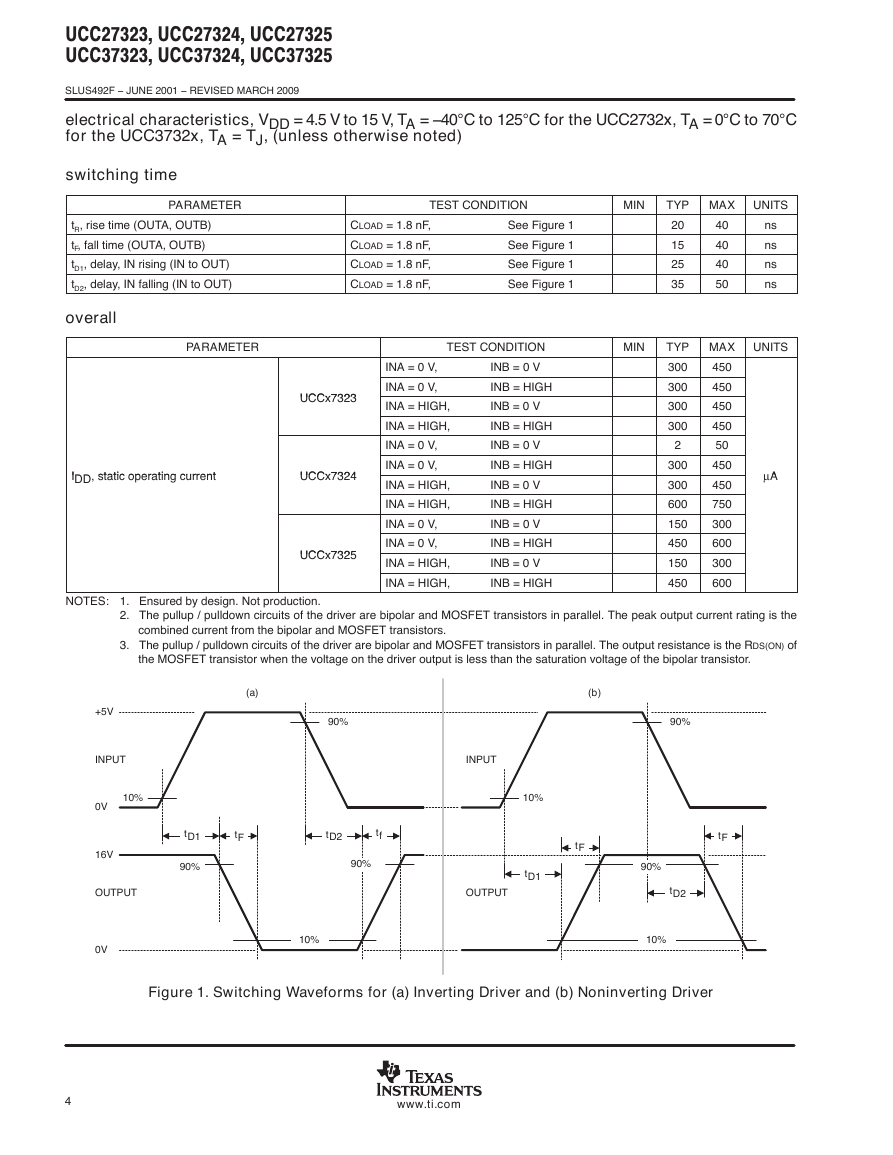
tR, rise time (OUTA, OUTB)
tF, fall time (OUTA, OUTB)
tD1, delay, IN rising (IN to OUT)
tD2, delay, IN falling (IN to OUT)
overall
PARAMETER
UCCx7323
UCCx7323
IDD, static operating current
IDD, static operating current
UCCx7324
UCCx7324
UCCx7325
UCCx7325
CLOAD = 1.8 nF,
CLOAD = 1.8 nF,
CLOAD = 1.8 nF,
CLOAD = 1.8 nF,
See Figure 1
See Figure 1
See Figure 1
See Figure 1
MIN
INA = 0 V,
INA = 0 V,
INA = HIGH,
INA = HIGH,
INA = 0 V,
INA = 0 V,
INA = HIGH,
INA = HIGH,
INA = 0 V,
INA = 0 V,
INA = HIGH,
INA = HIGH,
TEST CONDITION
INB = 0 V
INB = HIGH
INB = 0 V
INB = HIGH
INB = 0 V
INB = HIGH
INB = 0 V
INB = HIGH
INB = 0 V
INB = HIGH
INB = 0 V
INB = HIGH
NOTES: 1. Ensured by design. Not production.
2. The pullup / pulldown circuits of the driver are bipolar and MOSFET transistors in parallel. The peak output current rating is the
combined current from the bipolar and MOSFET transistors.
3. The pullup / pulldown circuits of the driver are bipolar and MOSFET transistors in parallel. The output resistance is the RDS(ON) of
the MOSFET transistor when the voltage on the driver output is less than the saturation voltage of the bipolar transistor.
(a)
90%
(b)
90%
tF
tD1
90%
tD2
tf
90%
10%
INPUT
OUTPUT
10%
tD1
tF
tF
90%
tD2
10%
+5V
INPUT
10%
0V
16V
OUTPUT
0V
Figure 1. Switching Waveforms for (a) Inverting Driver and (b) Noninverting Driver
4
www.ti.com
�
UCC27323, UCC27324, UCC27325
UCC37323, UCC37324, UCC37325
SLUS492F − JUNE 2001 − REVISED MARCH 2009
TERMINAL
NO.
NAME
1
2
3
4
5
6
7
8
N/C
INA
GND
INB
OUTB
VDD
OUTA
N/C
I/O
−
I
−
I
O
I
O
−
Terminal Functions
FUNCTION
FUNCTION
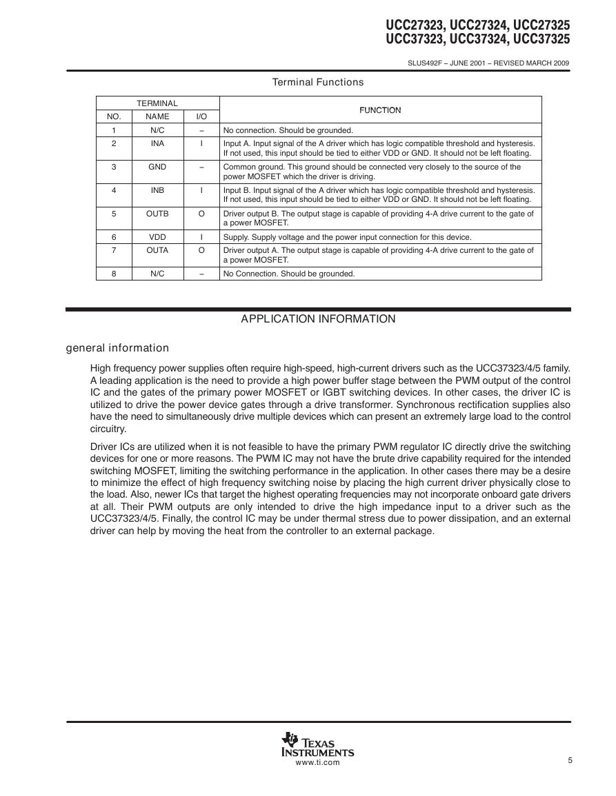
No connection. Should be grounded.
Input A. Input signal of the A driver which has logic compatible threshold and hysteresis.
If not used, this input should be tied to either VDD or GND. It should not be left floating.
Common ground. This ground should be connected very closely to the source of the
power MOSFET which the driver is driving.
Input B. Input signal of the A driver which has logic compatible threshold and hysteresis.
If not used, this input should be tied to either VDD or GND. It should not be left floating.
Driver output B. The output stage is capable of providing 4-A drive current to the gate of
a power MOSFET.
Supply. Supply voltage and the power input connection for this device.
Driver output A. The output stage is capable of providing 4-A drive current to the gate of
a power MOSFET.
No Connection. Should be grounded.
general information
APPLICATION INFORMATION
High frequency power supplies often require high-speed, high-current drivers such as the UCC37323/4/5 family.
A leading application is the need to provide a high power buffer stage between the PWM output of the control
IC and the gates of the primary power MOSFET or IGBT switching devices. In other cases, the driver IC is
utilized to drive the power device gates through a drive transformer. Synchronous rectification supplies also
have the need to simultaneously drive multiple devices which can present an extremely large load to the control
circuitry.
Driver ICs are utilized when it is not feasible to have the primary PWM regulator IC directly drive the switching
devices for one or more reasons. The PWM IC may not have the brute drive capability required for the intended
switching MOSFET, limiting the switching performance in the application. In other cases there may be a desire
to minimize the effect of high frequency switching noise by placing the high current driver physically close to
the load. Also, newer ICs that target the highest operating frequencies may not incorporate onboard gate drivers
at all. Their PWM outputs are only intended to drive the high impedance input to a driver such as the
UCC37323/4/5. Finally, the control IC may be under thermal stress due to power dissipation, and an external
driver can help by moving the heat from the controller to an external package.
www.ti.com
5
�
UCC27323, UCC27324, UCC27325
UCC37323, UCC37324, UCC37325
SLUS492F − JUNE 2001 − REVISED MARCH 2009
input stage
APPLICATION INFORMATION
The input thresholds have a 3.3−V logic sensitivity over the full range of VDD voltage; yet it is equally compatable
with 0 V to VDD signals.
The inputs of UCC37323/4/5 family of drivers are designed to withstand 500-mA reverse current without either
damage to the IC for logic upset. The input stage of each driver should be driven by a signal with a short rise
or fall time. This condition is satisfied in typical power supply applications, where the input signals are provided
by a PWM controller or logic gates with fast transition times (<200 ns). The input stages to the drivers function
as a digital gate, and they are not intended for applications where a slow changing input voltage is used to
generate a switching output when the logic threshold of the input section is reached. While this may not be
harmful to the driver, the output of the driver may switch repeatedly at a high frequency.
Users should not attempt to shape the input signals to the driver in an attempt to slow down (or delay) the signal
at the output. If limiting the rise or fall times to the power device is desired, limit the rise or fall times to the power
device, then an external resistance can be added between the output of the driver and the load device, which
is generally a power MOSFET gate. The external resistor may also help remove power dissipation from the IC
package, as discussed in the section on Thermal Considerations.
output stage
Inverting outputs of the UCC37323 and OUTA of the UCC37325 are intended to drive external P-channel
MOSFETs. Noninverting outputs of the UCC37324 and OUTB of the UCC37325 are intended to drive external
N-channel MOSFETs.
Each output stage is capable of supplying ±4-A peak current pulses and swings to both VDD and GND. The
pullup/ pulldown circuits of the driver are constructed of bipolar and MOSFET transistors in parallel. The peak
output current rating is the combined current from the bipolar and MOSFET transistors. The output resistance
is the RDS(on) of the MOSFET transistor when the voltage on the driver output is less than the saturation voltage
of the bipolar transistor. Each output stage also provides a very low impedance to overshoot and undershoot
due to the body diode of the internal MOSFET. This means that in many cases, external-schottky-clamp diodes
are not required.
The UCC37323 family delivers 4-A of gate drive where it is most needed during the MOSFET switching
transition – at the Miller plateau region – providing improved efficiency gains. A unique BiPolar and MOSFET
hybrid output stage in parallel also allows efficient current sourcing at low supply voltages.
6
www.ti.com
�
UCC27323, UCC27324, UCC27325
UCC37323, UCC37324, UCC37325
SLUS492F − JUNE 2001 − REVISED MARCH 2009
source/sink capabilities during Miller plateau
APPLICATION INFORMATION
Large power MOSFETs present a large load to the control circuitry. Proper drive is required for efficient, reliable
operation. The UCC37323/4/5 drivers have been optimized to provide maximum drive to a power MOSFET
during the Miller plateau region of the switching transition. This interval occurs while the drain voltage is swinging
between the voltage levels dictated by the power topology, requiring the charging/discharging of the drain-gate
capacitance with current supplied or removed by the driver IC. [1]
Two circuits are used to test the current capabilities of the UCC37323 driver. In each case external circuitry is
added to clamp the output near 5 V while the IC is sinking or sourcing current. An input pulse of 250 ns is applied
at a frequency of 1 kHz in the proper polarity for the respective test. In each test there is a transient period where
the current peaked up and then settled down to a steady-state value. The noted current measurements are
made at a time of 200 ns after the input pulse is applied, after the initial transient.
The first circuit in Figure 2 is used to verify the current sink capability when the output of the driver is clamped
around 5 V, a typical value of gate-source voltage during the Miller plateau region. The UCC37323 is found to
sink 4.5 A at VDD = 15 V and 4.28 A at VDD = 12 V.
VDD
INPUT
UCC37323
1
2
INA
OUTA
8
7
3
GND
VDD
6
INB
4
OUTB
5
DSCHOTTKY
10Ω
C2
1 µF
C3
100µF
+
VSUPPLY
5.5 V
VSNS
1 µF
CER
100µF
AL EL
RSNS
0.1Ω
Figure 2.
UDG−01065
www.ti.com
7
�
UCC27323, UCC27324, UCC27325
UCC37323, UCC37324, UCC37325
SLUS492F − JUNE 2001 − REVISED MARCH 2009
APPLICATION INFORMATION
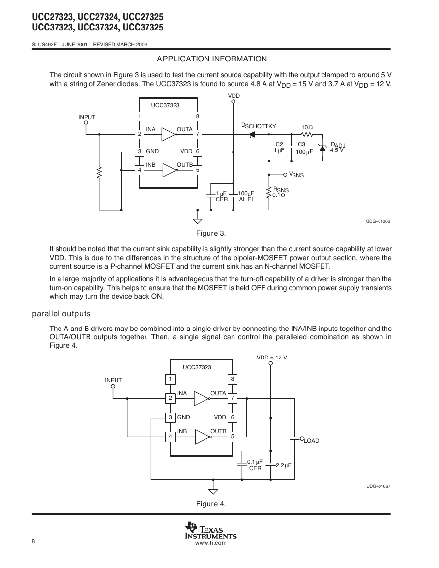
The circuit shown in Figure 3 is used to test the current source capability with the output clamped to around 5 V
with a string of Zener diodes. The UCC37323 is found to source 4.8 A at VDD = 15 V and 3.7 A at VDD = 12 V.
VDD
INPUT
UCC37323
1
2
INA
OUTA
8
7
3
GND
VDD
6
INB
4
OUTB
5
DSCHOTTKY
10Ω
C2
1 µF
C3
100 µF
DADJ
4.5 V
VSNS
1 µF
CER
100µF
AL EL
RSNS
0.1Ω
Figure 3.
UDG−01066
It should be noted that the current sink capability is slightly stronger than the current source capability at lower
VDD. This is due to the differences in the structure of the bipolar-MOSFET power output section, where the
current source is a P-channel MOSFET and the current sink has an N-channel MOSFET.
In a large majority of applications it is advantageous that the turn-off capability of a driver is stronger than the
turn-on capability. This helps to ensure that the MOSFET is held OFF during common power supply transients
which may turn the device back ON.
parallel outputs
The A and B drivers may be combined into a single driver by connecting the INA/INB inputs together and the
OUTA/OUTB outputs together. Then, a single signal can control the paralleled combination as shown in
Figure 4.
VDD = 12 V
INPUT
UCC37323
INA
OUTA
8
7
1
2
3
GND
VDD
6
INB
4
OUTB
5
8
Figure 4.
www.ti.com
CLOAD
0.1 µF
CER
2.2 µF
UDG−01067
�






 2023年江西萍乡中考道德与法治真题及答案.doc
 2012年重庆南川中考生物真题及答案.doc
 2013年江西师范大学地理学综合及文艺理论基础考研真题.doc
 2020年四川甘孜小升初语文真题及答案I卷.doc
 2020年注册岩土工程师专业基础考试真题及答案.doc
 2023-2024学年福建省厦门市九年级上学期数学月考试题及答案.doc
 2021-2022学年辽宁省沈阳市大东区九年级上学期语文期末试题及答案.doc
 2022-2023学年北京东城区初三第一学期物理期末试卷及答案.doc
 2018上半年江西教师资格初中地理学科知识与教学能力真题及答案.doc
 2012年河北国家公务员申论考试真题及答案-省级.doc
 2020-2021学年江苏省扬州市江都区邵樊片九年级上学期数学第一次质量检测试题及答案.doc
 2022下半年黑龙江教师资格证中学综合素质真题及答案.doc