JEDEC Standard No. 21-C
Page 4.1.2.11 – 1
Annex K: Serial Presence Detect (SPD) for DDR3 SDRAM Modules
SPD Revision 1.0
1.0 Introduction
This annex describes the serial presence detect (SPD) values for all DDR3 modules. Differences between module types
are encapsulated in subsections of this annex. These presence detect values are those referenced in the SPD standard
document for ‘Specific Features’. The following SPD fields will be documented in the order presented in section 1.1 with
the exception of bytes 60 ~ 116 which are documented in separate annexes, one for each family of module types. Fur-
ther description of Byte 2 is found in Annex A of the SPD standard. All unused entries will be coded as 0x00. All unused
bits in defined bytes will be coded as 0 except where noted.
To allow for maximum flexibility as devices evolve, SPD fields described in this document may support device configura-
tion and timing options that are not included in the JEDEC DDR3 SDRAM data sheet (JESD79-3). Please refer to DRAM
supplier data sheets or JESD79-3 to determine the compatibility of components.
1.1 Address map
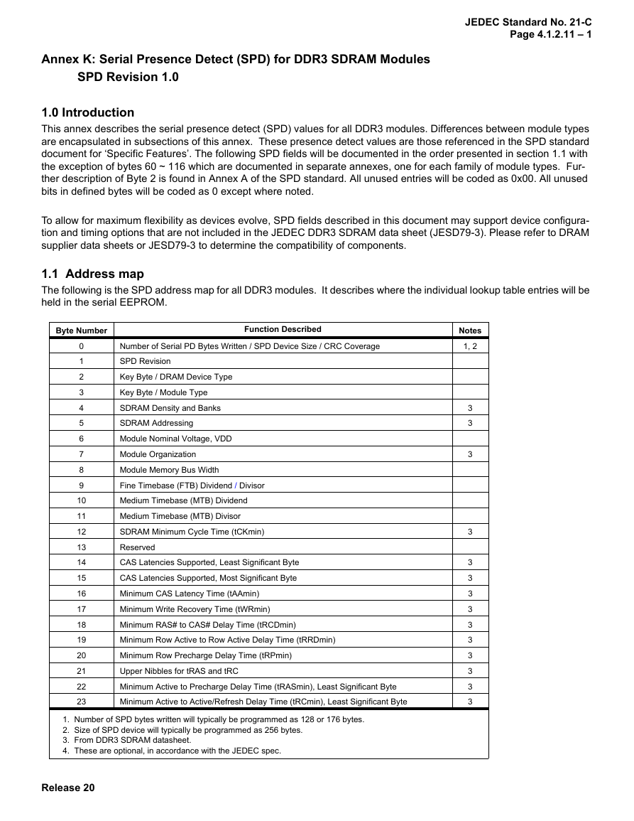
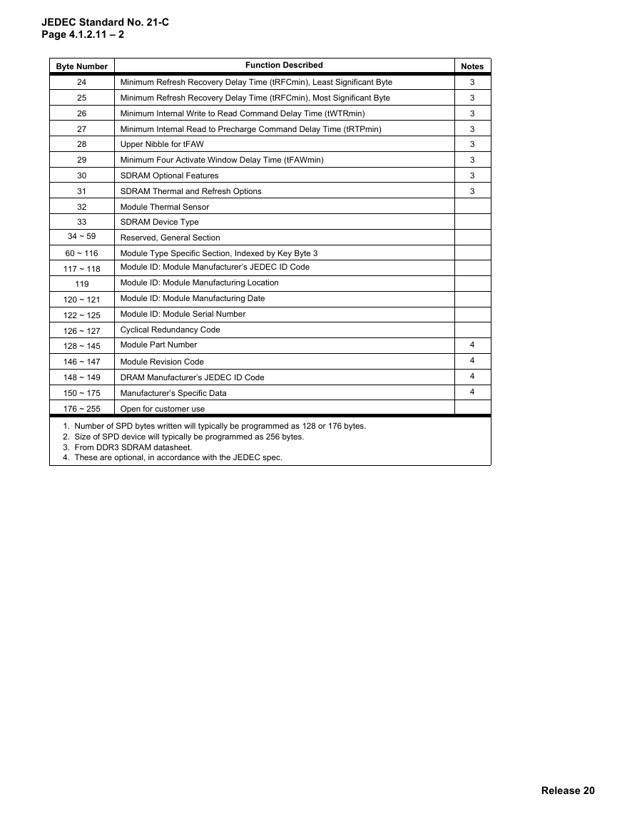
The following is the SPD address map for all DDR3 modules. It describes where the individual lookup table entries will be
held in the serial EEPROM.
Byte Number
Function Described
0
1
2
3
4
5
6
7
8
9
10
11
12
13
14
15
16
17
18
19
20
21
22
23
Number of Serial PD Bytes Written / SPD Device Size / CRC Coverage
SPD Revision
Key Byte / DRAM Device Type
Key Byte / Module Type
SDRAM Density and Banks
SDRAM Addressing
Module Nominal Voltage, VDD
Module Organization
Module Memory Bus Width
Fine Timebase (FTB) Dividend / Divisor
Medium Timebase (MTB) Dividend
Medium Timebase (MTB) Divisor
SDRAM Minimum Cycle Time (tCKmin)
Reserved
CAS Latencies Supported, Least Significant Byte
CAS Latencies Supported, Most Significant Byte
Minimum CAS Latency Time (tAAmin)
Minimum Write Recovery Time (tWRmin)
Minimum RAS# to CAS# Delay Time (tRCDmin)
Minimum Row Active to Row Active Delay Time (tRRDmin)
Minimum Row Precharge Delay Time (tRPmin)
Upper Nibbles for tRAS and tRC
Minimum Active to Precharge Delay Time (tRASmin), Least Significant Byte
Minimum Active to Active/Refresh Delay Time (tRCmin), Least Significant Byte
1. Number of SPD bytes written will typically be programmed as 128 or 176 bytes.
2. Size of SPD device will typically be programmed as 256 bytes.
3. From DDR3 SDRAM datasheet.
4. These are optional, in accordance with the JEDEC spec.
Release 20
Notes
1, 2
3
3
3
3
3
3
3
3
3
3
3
3
3
3
�
JEDEC Standard No. 21-C
Page 4.1.2.11 – 2
Byte Number
Function Described
Notes
24
25
26
27
28
29
30
31
32
33
34 ~ 59
60 ~ 116
117 ~ 118
119
120 ~ 121
122 ~ 125
126 ~ 127
128 ~ 145
146 ~ 147
148 ~ 149
150 ~ 175
176 ~ 255
Minimum Refresh Recovery Delay Time (tRFCmin), Least Significant Byte
Minimum Refresh Recovery Delay Time (tRFCmin), Most Significant Byte
Minimum Internal Write to Read Command Delay Time (tWTRmin)
Minimum Internal Read to Precharge Command Delay Time (tRTPmin)
Upper Nibble for tFAW
Minimum Four Activate Window Delay Time (tFAWmin)
SDRAM Optional Features
SDRAM Thermal and Refresh Options
Module Thermal Sensor
SDRAM Device Type
Reserved, General Section
Module Type Specific Section, Indexed by Key Byte 3
Module ID: Module Manufacturer’s JEDEC ID Code
Module ID: Module Manufacturing Location
Module ID: Module Manufacturing Date
Module ID: Module Serial Number
Cyclical Redundancy Code
Module Part Number
Module Revision Code
DRAM Manufacturer’s JEDEC ID Code
Manufacturer’s Specific Data
Open for customer use
1. Number of SPD bytes written will typically be programmed as 128 or 176 bytes.
2. Size of SPD device will typically be programmed as 256 bytes.
3. From DDR3 SDRAM datasheet.
4. These are optional, in accordance with the JEDEC spec.
3
3
3
3
3
3
3
3
4
4
4
4
Release 20
�
JEDEC Standard No. 21-C
Page 4.1.2.11 – 3
2.0 Details of each byte
2.1 General Section: Bytes 0 to 59
This section contains defines bytes that are common to all DDR3 module types.
Byte 0: Number of Bytes Used / Number of Bytes in SPD Device / CRC Coverage
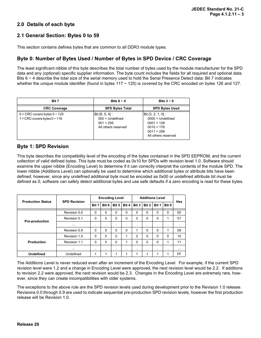
The least significant nibble of this byte describes the total number of bytes used by the module manufacturer for the SPD
data and any (optional) specific supplier information. The byte count includes the fields for all required and optional data.
Bits 6 ~ 4 describe the total size of the serial memory used to hold the Serial Presence Detect data. Bit 7 indicates
whether the unique module identifier (found in bytes 117 ~ 125) is covered by the CRC encoded on bytes 126 and 127.
Bit 7
CRC Coverage
Bits 6 ~ 4
Bits 3 ~ 0
SPD Bytes Total
SPD Bytes Used
0 = CRC covers bytes 0 ~ 125
1 = CRC covers bytes 0 ~ 116
Bit [6, 5, 4] :
000 = Undefined
001 = 256
All others reserved
Bit [3, 2, 1, 0] :
0000 = Undefined
0001 = 128
0010 = 176
0011 = 256
All others reserved
Byte 1: SPD Revision
This byte describes the compatibility level of the encoding of the bytes contained in the SPD EEPROM, and the current
collection of valid defined bytes. This byte must be coded as 0x10 for SPDs with revision level 1.0. Software should
examine the upper nibble (Encoding Level) to determine if it can correctly interpret the contents of the module SPD. The
lower nibble (Additions Level) can optionally be used to determine which additional bytes or attribute bits have been
defined; however, since any undefined additional byte must be encoded as 0x00 or undefined attribute bit must be
defined as 0, software can safely detect additional bytes and use safe defaults if a zero encoding is read for these bytes.
Production Status
SPD Revision
Pre-production
Production
Undefined
Revision 0.0
Revision 0.1
...
Revision 0.9
Revision 1.0
Revision 1.1
...
Undefined
Encoding Level
Additions Level
Bit 7 Bit 6 Bit 5 Bit 4 Bit 3 Bit 2 Bit 1 Bit 0
0
0
.
0
0
0
.
1
0
0
.
0
0
0
.
1
0
0
.
0
0
0
.
1
0
0
.
0
1
1
.
1
0
0
.
1
0
0
.
1
0
0
.
0
0
0
.
1
0
0
.
0
0
0
.
1
0
1
.
1
0
1
.
1
Hex
00
01
.
09
10
11
...
FF
The Additions Level is never reduced even after an increment of the Encoding Level. For example, if the current SPD
revision level were 1.2 and a change in Encoding Level were approved, the next revision level would be 2.2. If additions
to revision 2.2 were approved, the next revision would be 2.3. Changes in the Encoding Level are extremely rare, how-
ever, since they can create incompatibilities with older systems.
The exceptions to the above rule are the SPD revision levels used during development prior to the Revision 1.0 release.
Revisions 0.0 through 0.9 are used to indicate sequential pre-production SPD revision levels, however the first production
release will be Revision 1.0.
Release 20
�
JEDEC Standard No. 21-C
Page 4.1.2.11 – 4
Byte 2: Key Byte / DRAM Device Type
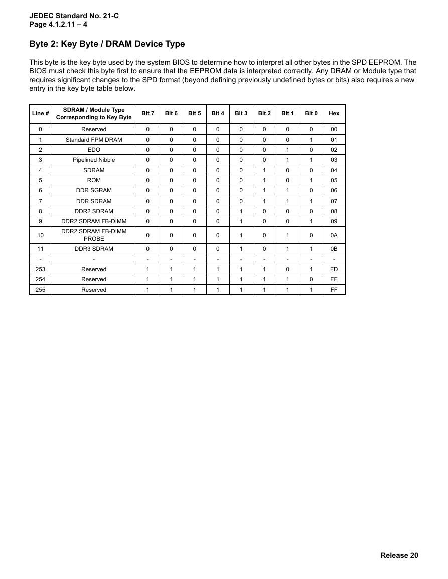
This byte is the key byte used by the system BIOS to determine how to interpret all other bytes in the SPD EEPROM. The
BIOS must check this byte first to ensure that the EEPROM data is interpreted correctly. Any DRAM or Module type that
requires significant changes to the SPD format (beyond defining previously undefined bytes or bits) also requires a new
entry in the key byte table below.
Line #
SDRAM / Module Type
Corresponding to Key Byte
Bit 7
Bit 6
Bit 5
Bit 4
Bit 3
Bit 2
Bit 1
Bit 0
Hex
0
1
2
3
4
5
6
7
8
9
10
11
-
253
254
255
Reserved
Standard FPM DRAM
EDO
Pipelined Nibble
SDRAM
ROM
DDR SGRAM
DDR SDRAM
DDR2 SDRAM
DDR2 SDRAM FB-DIMM
DDR2 SDRAM FB-DIMM
PROBE
DDR3 SDRAM
-
Reserved
Reserved
Reserved
0
0
0
0
0
0
0
0
0
0
0
0
-
1
1
1
0
0
0
0
0
0
0
0
0
0
0
0
-
1
1
1
0
0
0
0
0
0
0
0
0
0
0
0
-
1
1
1
0
0
0
0
0
0
0
0
0
0
0
0
-
1
1
1
0
0
0
0
0
0
0
0
1
1
1
1
-
1
1
1
0
0
0
0
1
1
1
1
0
0
0
0
-
1
1
1
0
0
1
1
0
0
1
1
0
0
1
1
-
0
1
1
0
1
0
1
0
1
0
1
0
1
0
1
-
1
0
1
00
01
02
03
04
05
06
07
08
09
0A
0B
-
FD
FE
FF
Release 20
�
JEDEC Standard No. 21-C
Page 4.1.2.11 – 5
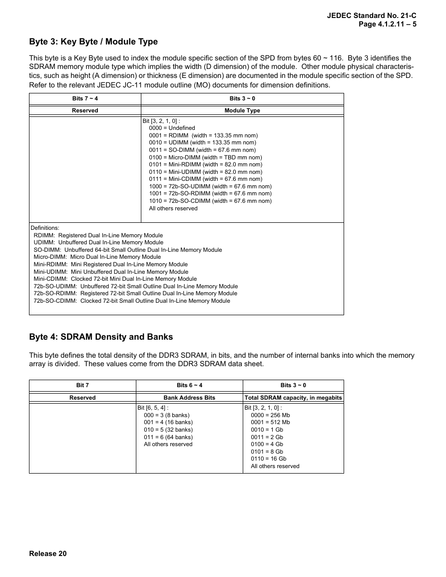
Byte 3: Key Byte / Module Type
This byte is a Key Byte used to index the module specific section of the SPD from bytes 60 ~ 116. Byte 3 identifies the
SDRAM memory module type which implies the width (D dimension) of the module. Other module physical characteris-
tics, such as height (A dimension) or thickness (E dimension) are documented in the module specific section of the SPD.
Refer to the relevant JEDEC JC-11 module outline (MO) documents for dimension definitions.
Bits 7 ~ 4
Reserved
Bits 3 ~ 0
Module Type
Bit [3, 2, 1, 0] :
0000 = Undefined
0001 = RDIMM (width = 133.35 mm nom)
0010 = UDIMM (width = 133.35 mm nom)
0011 = SO-DIMM (width = 67.6 mm nom)
0100 = Micro-DIMM (width = TBD mm nom)
0101 = Mini-RDIMM (width = 82.0 mm nom)
0110 = Mini-UDIMM (width = 82.0 mm nom)
0111 = Mini-CDIMM (width = 67.6 mm nom)
1000 = 72b-SO-UDIMM (width = 67.6 mm nom)
1001 = 72b-SO-RDIMM (width = 67.6 mm nom)
1010 = 72b-SO-CDIMM (width = 67.6 mm nom)
All others reserved
Definitions:
RDIMM: Registered Dual In-Line Memory Module
UDIMM: Unbuffered Dual In-Line Memory Module
SO-DIMM: Unbuffered 64-bit Small Outline Dual In-Line Memory Module
Micro-DIMM: Micro Dual In-Line Memory Module
Mini-RDIMM: Mini Registered Dual In-Line Memory Module
Mini-UDIMM: Mini Unbuffered Dual In-Line Memory Module
Mini-CDIMM: Clocked 72-bit Mini Dual In-Line Memory Module
72b-SO-UDIMM: Unbuffered 72-bit Small Outline Dual In-Line Memory Module
72b-SO-RDIMM: Registered 72-bit Small Outline Dual In-Line Memory Module
72b-SO-CDIMM: Clocked 72-bit Small Outline Dual In-Line Memory Module
Byte 4: SDRAM Density and Banks
This byte defines the total density of the DDR3 SDRAM, in bits, and the number of internal banks into which the memory
array is divided. These values come from the DDR3 SDRAM data sheet.
Bit 7
Reserved
Bits 6 ~ 4
Bank Address Bits
Bit [6, 5, 4] :
000 = 3 (8 banks)
001 = 4 (16 banks)
010 = 5 (32 banks)
011 = 6 (64 banks)
All others reserved
Bits 3 ~ 0
Total SDRAM capacity, in megabits
Bit [3, 2, 1, 0] :
0000 = 256 Mb
0001 = 512 Mb
0010 = 1 Gb
0011 = 2 Gb
0100 = 4 Gb
0101 = 8 Gb
0110 = 16 Gb
All others reserved
Release 20
�
JEDEC Standard No. 21-C
Page 4.1.2.11 – 6
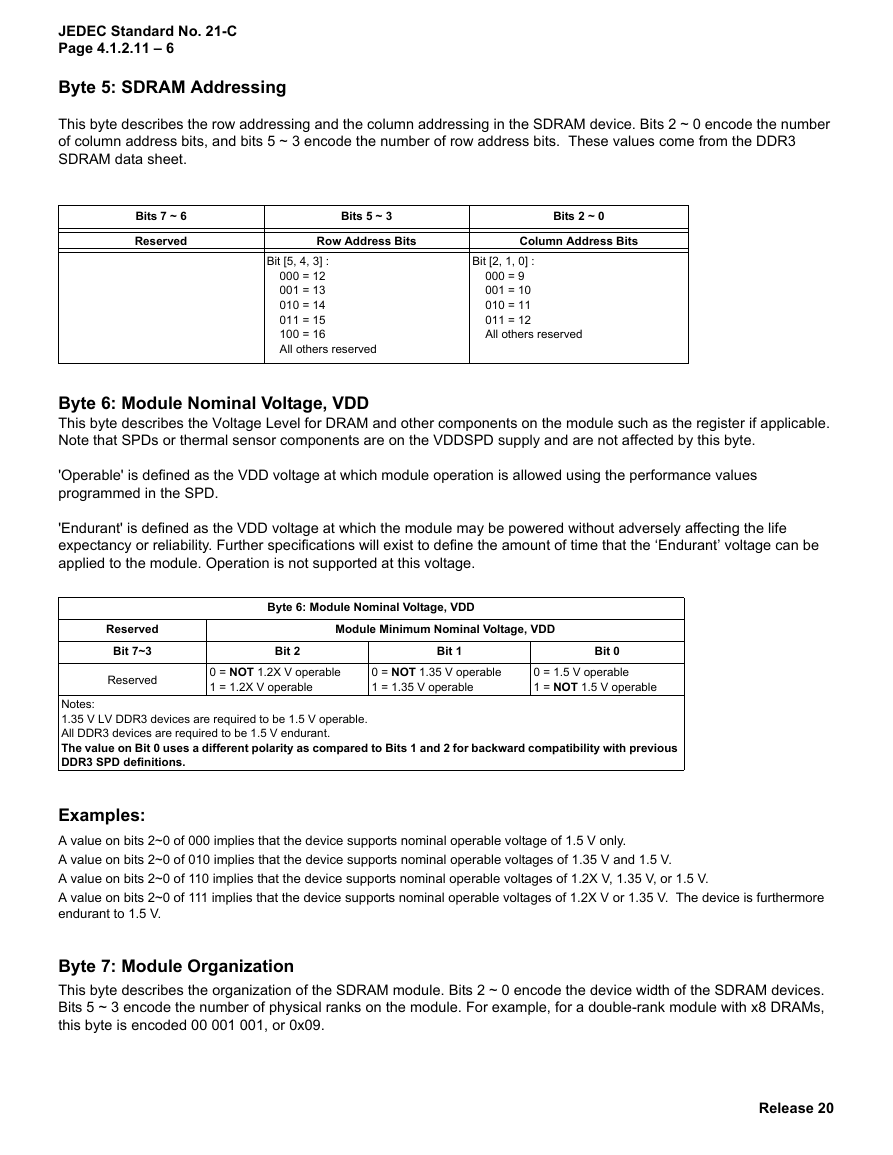
Byte 5: SDRAM Addressing
This byte describes the row addressing and the column addressing in the SDRAM device. Bits 2 ~ 0 encode the number
of column address bits, and bits 5 ~ 3 encode the number of row address bits. These values come from the DDR3
SDRAM data sheet.
Bits 7 ~ 6
Reserved
Bits 5 ~ 3
Row Address Bits
Bits 2 ~ 0
Column Address Bits
Bit [5, 4, 3] :
000 = 12
001 = 13
010 = 14
011 = 15
100 = 16
All others reserved
Bit [2, 1, 0] :
000 = 9
001 = 10
010 = 11
011 = 12
All others reserved
Byte 6: Module Nominal Voltage, VDD
This byte describes the Voltage Level for DRAM and other components on the module such as the register if applicable.
Note that SPDs or thermal sensor components are on the VDDSPD supply and are not affected by this byte.
'Operable' is defined as the VDD voltage at which module operation is allowed using the performance values
programmed in the SPD.
'Endurant' is defined as the VDD voltage at which the module may be powered without adversely affecting the life
expectancy or reliability. Further specifications will exist to define the amount of time that the ‘Endurant’ voltage can be
applied to the module. Operation is not supported at this voltage.
Reserved
Bit 7~3
Reserved
Byte 6: Module Nominal Voltage, VDD
Module Minimum Nominal Voltage, VDD
Bit 2
Bit 1
Bit 0
0 = NOT 1.2X V operable
1 = 1.2X V operable
0 = NOT 1.35 V operable
1 = 1.35 V operable
0 = 1.5 V operable
1 = NOT 1.5 V operable
Notes:
1.35 V LV DDR3 devices are required to be 1.5 V operable.
All DDR3 devices are required to be 1.5 V endurant.
The value on Bit 0 uses a different polarity as compared to Bits 1 and 2 for backward compatibility with previous
DDR3 SPD definitions.
Examples:
A value on bits 2~0 of 000 implies that the device supports nominal operable voltage of 1.5 V only.
A value on bits 2~0 of 010 implies that the device supports nominal operable voltages of 1.35 V and 1.5 V.
A value on bits 2~0 of 110 implies that the device supports nominal operable voltages of 1.2X V, 1.35 V, or 1.5 V.
A value on bits 2~0 of 111 implies that the device supports nominal operable voltages of 1.2X V or 1.35 V. The device is furthermore
endurant to 1.5 V.
Byte 7: Module Organization
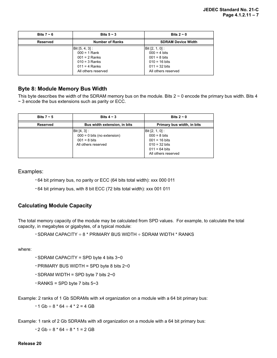
This byte describes the organization of the SDRAM module. Bits 2 ~ 0 encode the device width of the SDRAM devices.
Bits 5 ~ 3 encode the number of physical ranks on the module. For example, for a double-rank module with x8 DRAMs,
this byte is encoded 00 001 001, or 0x09.
Release 20
�
JEDEC Standard No. 21-C
Page 4.1.2.11 – 7
Bits 7 ~ 6
Reserved
Bits 5 ~ 3
Number of Ranks
Bits 2 ~ 0
SDRAM Device Width
Bit [5, 4, 3] :
000 = 1 Rank
001 = 2 Ranks
010 = 3 Ranks
011 = 4 Ranks
All others reserved
Bit [2, 1, 0] :
000 = 4 bits
001 = 8 bits
010 = 16 bits
011 = 32 bits
All others reserved
Byte 8: Module Memory Bus Width
This byte describes the width of the SDRAM memory bus on the module. Bits 2 ~ 0 encode the primary bus width. Bits 4
~ 3 encode the bus extensions such as parity or ECC.
Bits 7 ~ 5
Reserved
Bits 4 ~ 3
Bits 2 ~ 0
Bus width extension, in bits
Primary bus width, in bits
Bit [4, 3] :
000 = 0 bits (no extension)
001 = 8 bits
All others reserved
Bit [2, 1, 0] :
000 = 8 bits
001 = 16 bits
010 = 32 bits
011 = 64 bits
All others reserved
Examples:
•64 bit primary bus, no parity or ECC (64 bits total width): xxx 000 011
•64 bit primary bus, with 8 bit ECC (72 bits total width): xxx 001 011
Calculating Module Capacity
The total memory capacity of the module may be calculated from SPD values. For example, to calculate the total
capacity, in megabytes or gigabytes, of a typical module:
•SDRAM CAPACITY ÷ 8 * PRIMARY BUS WIDTH ÷ SDRAM WIDTH * RANKS
where:
•SDRAM CAPACITY = SPD byte 4 bits 3~0
•PRIMARY BUS WIDTH = SPD byte 8 bits 2~0
•SDRAM WIDTH = SPD byte 7 bits 2~0
•RANKS = SPD byte 7 bits 5~3
Example: 2 ranks of 1 Gb SDRAMs with x4 organization on a module with a 64 bit primary bus:
•1 Gb ÷ 8 * 64 ÷ 4 * 2 = 4 GB
Example: 1 rank of 2 Gb SDRAMs with x8 organization on a module with a 64 bit primary bus:
•2 Gb ÷ 8 * 64 ÷ 8 * 1 = 2 GB
Release 20
�
JEDEC Standard No. 21-C
Page 4.1.2.11 – 8
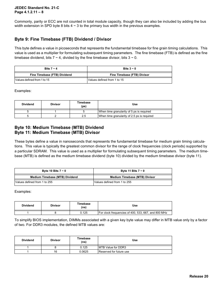
Commonly, parity or ECC are not counted in total module capacity, though they can also be included by adding the bus
width extension in SPD byte 8 bits 4 ~ 3 to the primary bus width in the previous examples.
Byte 9: Fine Timebase (FTB) Dividend / Divisor
This byte defines a value in picoseconds that represents the fundamental timebase for fine grain timing calculations. This
value is used as a multiplier for formulating subsequent timing parameters. The fine timebase (FTB) is defined as the fine
timebase dividend, bits 7 ~ 4, divided by the fine timebase divisor, bits 3 ~ 0.
Bits 7 ~ 4
Bits 3 ~ 0
Fine Timebase (FTB) Dividend
Fine Timebase (FTB) Divisor
Values defined from 1 to 15 Values defined from 1 to 15
Examples:
Dividend
Divisor
5
5
1
2
Timebase
(ps)
5
2.5
Use
When time granularity of 5 ps is required
When time granularity of 2.5 ps is required
Byte 10: Medium Timebase (MTB) Dividend
Byte 11: Medium Timebase (MTB) Divisor
These bytes define a value in nanoseconds that represents the fundamental timebase for medium grain timing calcula-
tions. This value is typically the greatest common divisor for the range of clock frequencies (clock periods) supported by
a particular SDRAM. This value is used as a multiplier for formulating subsequent timing parameters. The medium time-
base (MTB) is defined as the medium timebase dividend (byte 10) divided by the medium timebase divisor (byte 11).
Byte 10 Bits 7 ~ 0
Byte 11 Bits 7 ~ 0
Medium Timebase (MTB) Dividend
Medium Timebase (MTB) Divisor
Values defined from 1 to 255
Values defined from 1 to 255
Examples:
Dividend
1
Divisor
8
Timebase
(ns)
0.125
Use
For clock frequencies of 400, 533, 667, and 800 MHz
To simplify BIOS implementation, DIMMs associated with a given key byte value may differ in MTB value only by a factor
of two. For DDR3 modules, the defined MTB values are:
Dividend
Divisor
1
1
8
16
Timebase
(ns)
0.125
0.0625
Use
MTB Value for DDR3
Reserved for future use
Release 20
�


 2023年江西萍乡中考道德与法治真题及答案.doc
 2012年重庆南川中考生物真题及答案.doc
 2013年江西师范大学地理学综合及文艺理论基础考研真题.doc
 2020年四川甘孜小升初语文真题及答案I卷.doc
 2020年注册岩土工程师专业基础考试真题及答案.doc
 2023-2024学年福建省厦门市九年级上学期数学月考试题及答案.doc
 2021-2022学年辽宁省沈阳市大东区九年级上学期语文期末试题及答案.doc
 2022-2023学年北京东城区初三第一学期物理期末试卷及答案.doc
 2018上半年江西教师资格初中地理学科知识与教学能力真题及答案.doc
 2012年河北国家公务员申论考试真题及答案-省级.doc
 2020-2021学年江苏省扬州市江都区邵樊片九年级上学期数学第一次质量检测试题及答案.doc
 2022下半年黑龙江教师资格证中学综合素质真题及答案.doc