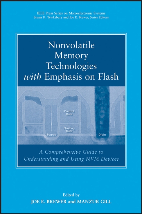
NONVOLATILE MEMORY TECHNOLOGIES WITH EMPHASIS ON FLASH
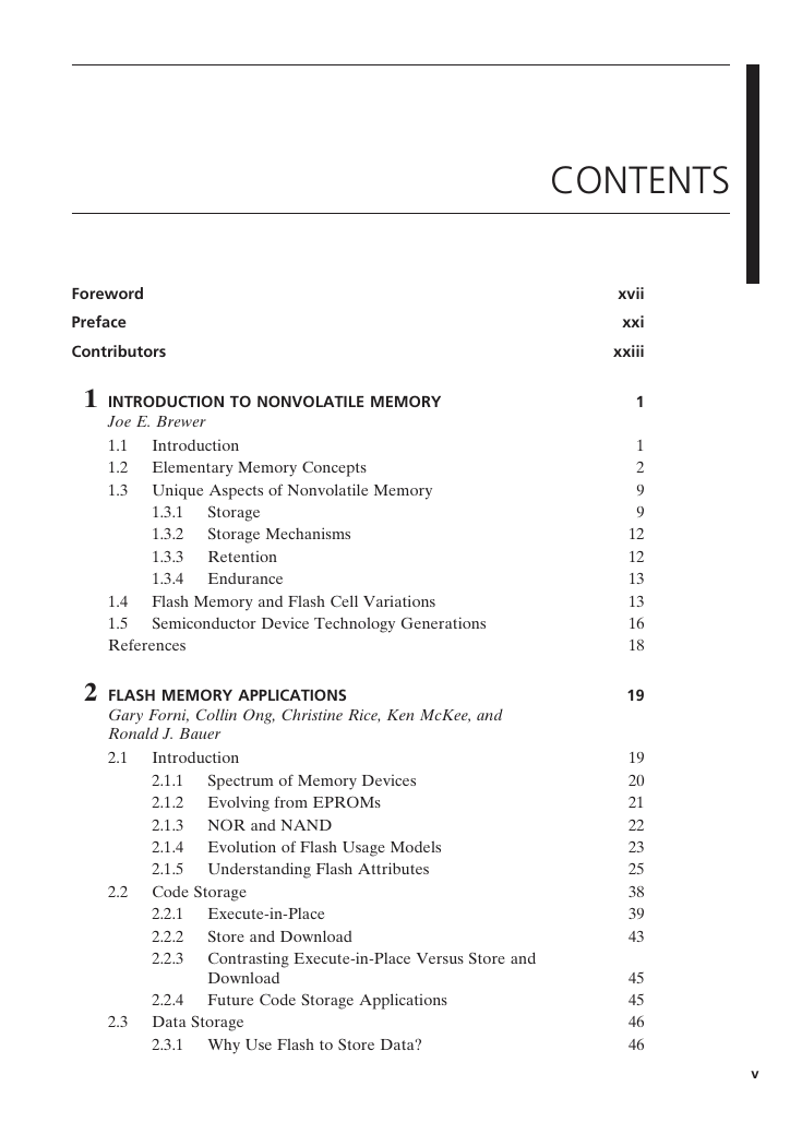
CONTENTS
Foreword
Preface
Contributors
1 INTRODUCTION TO NONVOLATILE MEMORY
1.1 Introduction
1.2 Elementary Memory Concepts
1.3 Unique Aspects of Nonvolatile Memory
1.3.1 Storage
1.3.2 Storage Mechanisms
1.3.3 Retention
1.3.4 Endurance
1.4 Flash Memory and Flash Cell Variations
1.5 Semiconductor Device Technology Generations
References
2 FLASH MEMORY APPLICATIONS
2.1 Introduction
2.1.1 Spectrum of Memory Devices
2.1.2 Evolving from EPROMs
2.1.3 NOR and NAND
2.1.4 Evolution of Flash Usage Models
2.1.5 Understanding Flash Attributes
2.2 Code Storage
2.2.1 Execute-in-Place
2.2.2 Store and Download
2.2.3 Contrasting Execute-in-Place Versus Store and Download
2.2.4 Future Code Storage Applications
2.3 Data Storage
2.3.1 Why Use Flash to Store Data?
2.3.2 Architectural Decisions
2.3.3 Embedded Flash Storage
2.3.4 Removable Media
2.4 Code+Data Storage
2.4.1 Relevant Attributes for Code+Data
2.4.2 Fitting the Pieces Together for Code+Data
2.4.3 Benefits of Code+Data
2.5 Conclusion
3 MEMORY CIRCUIT TECHNOLOGIES
3.1 Introduction
3.2 Flash Cell Basic Operation
3.2.1 Cell Programming
3.2.2 Cell Erase
3.2.3 Compaction
3.2.4 Read
3.3 Flash Memory Architecture
3.3.1 Memory Cell Array
3.3.2 Analog Blocks
3.3.3 Control Logic
3.4 Redundancy
3.4.1 Defectivity and Process Variations
3.4.2 Yield Improvement
3.4.3 Yield Simulator
3.4.4 Redundancy Fuses Design
3.4.5 Row Redundancy Design
3.4.6 Column Redundancy Design
3.4.7 Advanced Redundancy Design
3.5 Error Correction Coding (ECC)
3.5.1 On-Chip ECC and Endurance/Retention in Flash Memories
3.5.2 On-Chip ECC and Multilevel Flash Memories
3.6 Design for Testability (DFT)
3.6.1 Test Entry and Organization
3.6.2 Fuse Cell
3.6.3 Sense Amplifier Reference Trimming and Monitor
3.6.4 High Voltages Trimming
3.6.5 Timings Trimming and External Control
3.6.6 Internal State Machine Algorithm Skips and Monitor
3.6.7 Address Path Configuration
3.6.8 Data Path Configuration and Trimming
3.6.9 High Voltages External Forcing and Monitor
3.6.10 Array Direct Access and Stresses
3.6.11 Internal Pattern Write and Verify
3.6.12 Data Compression
3.7 Flash-Specific Circuit Techniques
3.7.1 Voltage Level Shifting
3.7.2 Sensing
3.7.3 Voltage Multiplication
3.7.4 Reference Voltage Generation
3.7.5 Voltage Regulation
3.7.6 I/O Signal Buffering
References
4 PHYSICS OF FLASH MEMORIES
4.1 Introduction
4.2 Basic Operating Principles and Memory Characteristics
4.2.1 Floating-Gate Principle
4.2.2 Basic Definitions with Examples
4.2.3 Basic Equations and Models
4.3 Physics of Programming and Erase Mechanisms
4.3.1 Fowler–Nordheim Tunneling
4.3.2 Polyoxide Conduction
4.3.3 Channel Hot-Electron Injection (CHEI)
4.3.4 Substrate Hot-Electron Injection (SHEI)
4.3.5 Source-Side Injection (SSI)
4.3.6 Secondary Impact Ionization Initiated Channel Hot-Electron Injection
4.4 Physics of Degradation and Disturb Mechanisms
4.4.1 Band-to-Band Tunneling
4.4.2 Oxide Degradation
4.4.3 Oxide Breakdown
4.5 Conclusion
References
5 NOR FLASH STACKED AND SPLIT-GATE MEMORY TECHNOLOGY
5.1 Introduction
5.2 ETOX Flash Cell Technology
5.2.1 Introduction
5.2.2 Cell Structure
5.2.3 Read (Sensing)
5.2.4 Programming
5.2.5 Erasing
5.2.6 Array Operation
5.2.7 Erase Threshold Control
5.2.8 Process and Scaling Issues
5.2.9 Key Circuits and Circuit/Technology Interactions
5.2.10 Multilevel Cell Technology Circuits
5.3 SST SuperFlash EEPROM Cell Technology
5.3.1 Introduction
5.3.2 Cell Cross Sections and Layout
5.3.3 Charge Transfer Mechanisms
5.3.4 Erase
5.3.5 Programming
5.3.6 Cell Array Architecture and Operation
5.3.7 Erase Threshold Control and Distribution
5.3.8 Process Scaling Issues
5.3.9 Key Circuit Interactions
5.3.10 Multilevel Cell Implementation
5.4 Reliability Issues and Solutions
5.4.1 Oxide Integrity
5.4.2 Contact Integrity
5.4.3 Data Retention
5.4.4 Endurance
5.4.5 Disturbs
5.4.6 Life Test (Dynamic Burn-in)
5.5 Applications
References
6 NAND FLASH MEMORY TECHNOLOGY
6.1 Overview of NAND EEPROM
6.2 NAND Cell Operation
6.2.1 Cell Structure
6.2.2 Erase Operation
6.2.3 Program Operation
6.2.4 Program Disturb
6.2.5 Read Operation
6.3 NAND Array Architecture and Operation
6.3.1 Staggered Row Decoder
6.3.2 Self-Boosted Erase Inhibit Scheme
6.3.3 Self-Boosted Program Inhibit Scheme
6.3.4 Read Operation
6.4 Program Threshold Control and Program V(t) Spread Reduction
6.4.1 Bit-by-Bit Verify Circuit
6.4.2 Sophisticated Bit-by-Bit Verify Circuit
6.4.3 Overprogram Elimination Scheme
6.5 Process and Scaling Issues
6.5.1 Shallow Trench Isolation NAND Technology (256-Mbit NAND)
6.5.2 Booster Plate Technology
6.5.3 Channel Boost Capacitance Cell
6.5.4 Negative V(th) Cell
6.5.5 Free Wordline Spacing Cell
6.6 Key Circuits and Circuit/Technology Interactions
6.6.1 Shielded Bitline Sensing Method
6.6.2 Full Chip Burst Read Operation
6.6.3 Symmetric Sense Amplifier with Page Copy Function
6.6.4 Source Line Programming Scheme
6.7 Multilevel NAND
6.7.1 Multilevel Circuit Technology
6.7.2 Array Noise Suppression Technology
6.7.3 Side-Wall Transfer Transistor Cell
6.7.4 Three-Level NAND
6.7.5 High-Speed Programming
References
Bibliography
7 DINOR FLASH MEMORY TECHNOLOGY
7.1 Introduction
7.2 DINOR Operation and Array Architecture
7.2.1 DINOR Operation
7.2.2 DINOR Cell Characteristics
7.2.3 DINOR Array Architecture
7.2.4 DINOR Advanced Array Architecture
7.2.5 VGA-DINOR Device Structure and Fabrication
7.2.6 Characteristics of the Cell with Asymmetrical Offset Source/Drain Structure
7.3 DINOR Technology Features
7.3.1 Low-Voltage Read
7.3.2 Fast Read Access
7.4 DINOR Circuit for Low-Voltage Operation
7.4.1 High-Voltage Generation [7]
7.4.2 Wordline Boost Scheme
7.5 Background Operation Function
7.5.1 Background Operation and DINOR
7.5.2 Emulating Electrically Erasable Programmable Read-Only Memory (EEPROM) and Static Random-Access Memory (SRAM)
7.5.3 Background Operation Fast Erase
7.6 P-Channel DINOR Architecture
7.6.1 Introduction
7.6.2 Band-to-Band Hot-Electron Injection Cell Operation
7.6.3 DINOR BBHE Programmed Cell
7.6.4 P-Channel DINOR Summary
References
Bibliography
8 P-CHANNEL FLASH MEMORY TECHNOLOGY
8.1 Introduction
8.2 Device Structure
8.3 Operations of P-Channel Flash
8.4 Array Architecture of P-Channel Flash
8.4.1 NOR-Type Array Architecture
8.4.2 NAND-Type Array Architecture
8.5 Evolution of P-Channel Flash
8.5.1 Hsu et al. [1]
8.5.2 Ohnakado et al. [4]
8.5.3 Ohnakado et al. [5]
8.5.4 Shen et al. [6]
8.5.5 Chung et al. [7]
8.5.6 Sarin et al. [8]
8.5.7 Wang et al. [9]
8.5.8 Ohnakado et al. [2]
8.5.9 For Further Study
8.6 Processing Technology for P-Channel Flash
8.6.1 NOR-Type Array Architecture
8.6.2 NAND-Type Array Architecture
References
Bibliography
9 EMBEDDED FLASH MEMORY
9.1 Introduction
9.2 Embedded Flash Versus Stand-Alone Flash Memory
9.2.1 Advantages of Embedded over Stand-Alone Flash Memory
9.2.2 Disadvantages of Embedded over Stand-Alone Flash Memory
9.3 Embedded Flash Memory Applications
9.3.1 Applications by Device Type
9.3.2 Applications by Function
9.3.3 Applications by End Product
9.3.4 Applications by Usage
9.4 Embedded Flash Memory Cells
9.4.1 Special Requirements and Considerations
9.4.2 Cell Selection for Embedded Applications
9.5 Embedded Flash Memory Design
9.5.1 Special Requirements and Consideration
9.5.2 Flash Module Design for Embedded Applications
9.5.3 Design Techniques for Embedded Flash Module
References
10 TUNNEL DIELECTRICS FOR SCALED FLASH MEMORY CELLS
10.1 Introduction
10.2 SiO(2) as Tunnel Dielectric—Historical Perspective
10.3 Early Work on Silicon Nitride as a Tunnel Dielectric
10.4 Jet-Vapor Deposition Silicon Nitride Deposition
10.5 Properties of Gate-Quality JVD Silicon Nitride Films
10.6 Deposited Silicon Nitride as Tunnel Dielectric
10.7 N-Channel Floating-Gate Device with Deposited Silicon Nitride Tunnel Dielectric
10.8 P-Channel Floating-Gate Device with Deposited Silicon Nitride Tunnel Dielectric
10.9 Reliability Concerns Associated with Hot-Hole Injection
10.10 Tunnel Dielectric for SONOS Cell
10.11 Prospects for High-K Dielectrics
10.12 Tunnel Barrier Engineering with Multiple Barriers
10.12.1 Crested Barrier
10.12.2 U-Shaped Barrier
10.13 Summary
References
11 FLASH MEMORY RELIABILITY
11.1 Introduction
11.2 Cycling-Induced Degradations in Flash Memories
11.2.1 Overview of Cycling-Induced Degradations
11.2.2 Channel Hot-Electron Programming-Induced Oxide Degradation
11.2.3 Tunnel-Erase-Induced Oxide Degradation
11.2.4 Erratic Erase
11.3 Flash Memory Data Retention
11.3.1 Activation Energy and Accelerated Data Retention Bake Tests
11.3.2 Charge-Loss and Gain Mechanisms in EPROMs and Flash EPROMs
11.3.3 Flash EEPROM Cycling-Induced Data Retention Issues
11.3.4 Data Retention Characteristics Related to Tunnel Oxide and Floating-Gate Poly Texture
11.3.5 Soft Errors
11.4 Flash Memory Disturbs
11.4.1 Read Disturb and the Effects of Cycling
11.4.2 Program Disturb
11.4.3 Erase Disturb
11.4.4 Block-to-Block Disturbs
11.5 Stress-Induced Tunnel Oxide Leakage Current
11.5.1 Uniform SILC in Thin Oxide
11.5.2 SILC in Thin Oxide after Bipolarity Stress
11.5.3 Microscopic Characteristics of Stress-Induced Leakage Current (mSILC)
11.5.4 Stress-Induced Leakage Current in Oxynitride
11.5.5 Stress-Induced Leakage Current as the Limiting Factor for Tunnel Oxide Scaling
11.6 Special Reliability Issues for Poly-to-Poly Erase and Source-Side Injection Program
11.6.1 Poly-to-Poly Erase and Its Reliability Issues
11.6.2 Source-Side Injection and Its Reliability Issues
11.7 Process Impacts on Flash Memory Reliability
11.7.1 Tunnel Oxide Process and Nitrogen Incorporation
11.7.2 Effects of Floating-Gate Process and Morphology
11.7.3 Stacked Gate SAS (Self-Aligned Source) Etch Process and Erase Distribution
11.7.4 In-Line Plasma Charging Damage
11.7.5 Impacts of Intermetal Dielectric and Passivation Films on Flash Memory Reliability
11.8 High-Voltage Periphery Transistor Reliability
11.8.1 High-Voltage Transistor Technology
11.8.2 Reliability of HV Transistors in Flash Memory Products
11.8.3 Process Defects: The Role of Cycling and Burn-in
11.9 Design and System Impacts on Flash Memory Reliability
11.9.1 Embedded Erase and Program Algorithm
11.9.2 Redundancy and Defect Mapping
11.9.3 Error Correction Concepts and Techniques
11.9.4 Wear Leveling
11.10 Flash Memory Reliability Screening and Qualification
11.10.1 Introduction to Reliability Testing and Screening
11.10.2 Classification of Flash Memory Reliability Tests
11.10.3 Acceleration Models of the Reliability Tests
11.10.4 Flash Memory Sort and Reliability Test Flow
11.10.5 Flash Memory Product Qualification Flow
11.10.6 Burn-In and Reliability Monitoring Program
11.10.7 Failure Rate Calculations
11.11 For Further Study
11.11.1 Introduction
11.11.2 Erratic Erase
11.11.3 Stress-Induced-Leakage-Current Related Retention Effects
11.11.4 Detrapping-Related Retention Effects
11.11.5 Qualification Methods
11.11.6 Flash Memory Floating-Gate to Floating-Gate Coupling
11.11.7 New Program Disturb Phenomenon in NAND Flash Memory
11.11.8 Impacts of Random Telegraph Signals and Few-Electron Phenomena on the Scaling of Flash Memories
References
12 MULTILEVEL CELL DIGITAL MEMORIES
12.1 Introduction
12.2 Pursuit of Low-Cost Memory
12.3 Multibit Storage Breakthrough
12.3.1 Intel StrataFlash Technology
12.3.2 Evolution of MLC Memory Technology Development
12.3.3 Multilevel Cell Concept
12.4 View of MLC Today
12.4.1 Multilevel Cell Key Features
12.4.2 Flash Cell Structure and Operation
12.4.3 Multilevel Cell Operation
12.4.4 Mixed Signal Design Implementation
12.5 Low-Cost Design Implementation
12.6 Low-Cost Process Manufacturing
12.7 Standard Product Feature Set
12.7.1 Programming Speed
12.7.2 Read Speed
12.7.3 Power Supply
12.7.4 Reliability
12.8 Further Reading: Multilevel Flash Memory and Technology Scaling
12.9 Conclusion
References
13 ALTERNATIVE MEMORY TECHNOLOGIES
13.1 Introduction
13.2 Limitations of Flash Memory
13.2.1 Introduction
13.2.2 Programming Voltage
13.2.3 Programming Speed
13.2.4 Endurance
13.2.5 Scaling
13.3 NROM Memories
13.3.1 Introduction
13.3.2 Memory Cell and Array; Structure and Operation
13.3.3 Storage Mechanism
13.3.4 Reliability
13.3.5 Quad NROM Technology
13.3.6 Fabrication
13.3.7 Scaling
13.3.8 Products
13.3.9 Summary
13.4 Ferroelectric Memories
13.4.1 Introduction
13.4.2 Storage Mechanism
13.4.3 Memory Cells and Arrays
13.4.4 Fabrication
13.4.5 Nonvolatile Characteristics
13.4.6 Scaling
13.4.7 Reliability
13.4.8 Die and Test Cost
13.4.9 Ferroelectric Products
13.4.10 Ferroelectric Memory Summary
13.5 Magnetic Memories
13.5.1 Introduction
13.5.2 Magnetic Random-Access Memory with Giant Magnetoresistive Devices
13.5.3 Magnetic Random-Access Memory with Magnetic Tunnel Junction Devices
13.5.4 Programming Characteristics
13.5.5 Fabrication
13.5.6 Nonvolatile Characteristics
13.5.7 Scaling
13.5.8 Reliability
13.5.9 Die and Test Cost
13.5.10 Magnetic Memory Summary
13.6 Single-Electron and Few-Electron Memories
13.6.1 Introduction
13.6.2 Electric Charge Quantization in Solids
13.6.3 Single-Electron Effects in Memory Cells
13.6.4 Single-Electron Memories
13.6.5 Few-Electron Memories
13.7 Resistive and Hybrid CMOS/Nanodevice Memories
13.7.1 Introduction
13.7.2 Programmable Diode Technologies
13.7.3 Hybrid CMOS/Nanodevice Resistive Memories
13.7.4 Expected Performance
13.7.5 Resistive Memory Summary
13.8 NOVORAM/FGRAM Cell and Architecture
13.8.1 Introduction
Untitled
13.8.2 Crested Tunnel Barriers
13.8.3 NOVORAM/FGRAM Cell and Architecture
13.8.4 NOVORAM/FGRAM Summary
13.9 Phase Change Memories
13.9.1 Introduction
13.9.2 Storage Mechanism
13.9.3 GST Phase Change Material
13.9.4 Memory Cell
13.9.5 Memory Array and Support Circuitry
13.9.6 Fabrication
13.9.7 Scaling
13.9.8 Reliability
13.9.9 Products
13.9.10 Summary
References
Index
About the Editors




 2023年江西萍乡中考道德与法治真题及答案.doc
 2012年重庆南川中考生物真题及答案.doc
 2013年江西师范大学地理学综合及文艺理论基础考研真题.doc
 2020年四川甘孜小升初语文真题及答案I卷.doc
 2020年注册岩土工程师专业基础考试真题及答案.doc
 2023-2024学年福建省厦门市九年级上学期数学月考试题及答案.doc
 2021-2022学年辽宁省沈阳市大东区九年级上学期语文期末试题及答案.doc
 2022-2023学年北京东城区初三第一学期物理期末试卷及答案.doc
 2018上半年江西教师资格初中地理学科知识与教学能力真题及答案.doc
 2012年河北国家公务员申论考试真题及答案-省级.doc
 2020-2021学年江苏省扬州市江都区邵樊片九年级上学期数学第一次质量检测试题及答案.doc
 2022下半年黑龙江教师资格证中学综合素质真题及答案.doc