100 Gbit/s Scrambler Architectures for OTN Protocol:
FPGA Implementation and Result Comparison
Arley Salvador, Valentino Corso
CPqD Research and Development Center in Telecommunications
Campinas, Brazil
arleys@cpqd.com.br
Abstract— This paper describes and compares two scrambler
architectures developed and implemented in an advanced field
programmable gate array
in
100 Gbit/s optical transport network (OTN) systems.
(FPGA), with applications
I.
INTRODUCTION
Due to the increasing utilization of channel bandwidth
combined with the necessity to concentrate and control data
in optical communication transmission systems, resulted on a
standardized transmission protocol by ITU-T (International
Telecommunication Union) G.709 [1]. This recommendation
defines the network interfaces for optical fiber links up to 100
Gbit/s. In these optical transport network (OTN) systems,
clock signals are recovered from the incoming data stream
and, long sequences of consecutive digits (zeros or ones) are
avoided through the use of digital scrambling techniques. Due
to the complexity of OTN equipment devices, designers avoid
the over-consumption of logic resources. This paper presents
a comparison between two different low gate count scrambler
architectures and indicates the most suitable solution.
scrambler
logic
Section II briefly describes the OTN scrambler, according
to the recommendation specifications. Section III and IV
implemented with
present
combinational
registers
(registered scrambler), respectively. The comparison of these
two architectures
in section V. Finally,
conclusions are shown in section VI.
architectures
(logical scrambler) and
is presented
II. OTN SCRAMBLER
A scrambler module performs data scrambling by
implementing an exclusive-OR operation between two data
streams: the transmitted information and the pseudorandom
bit sequence (PRBS) generator.
The OTN scrambler
is described by ITU-T G.709
recommendation [1] and uses the polynomial x16 + x12 + x3 +
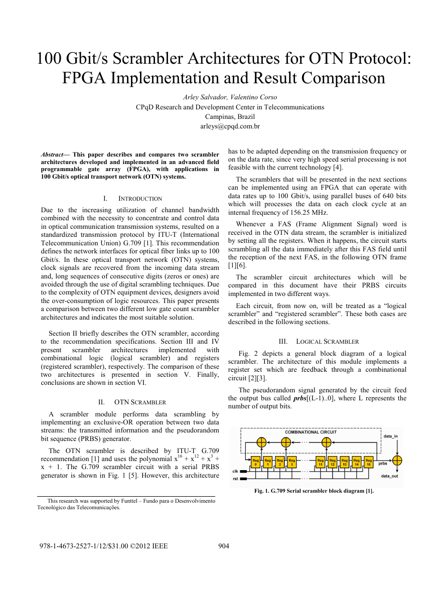
x + 1. The G.709 scrambler circuit with a serial PRBS
generator is shown in Fig. 1 [5]. However, this architecture
This research was supported by Funttel – Fundo para o Desenvolvimento
Tecnológico das Telecomunicações.
has to be adapted depending on the transmission frequency or
on the data rate, since very high speed serial processing is not
feasible with the current technology [4].
The scramblers that will be presented in the next sections
can be implemented using an FPGA that can operate with
data rates up to 100 Gbit/s, using parallel buses of 640 bits
which will processes the data on each clock cycle at an
internal frequency of 156.25 MHz.
Whenever a FAS (Frame Alignment Signal) word is
received in the OTN data stream, the scrambler is initialized
by setting all the registers. When it happens, the circuit starts
scrambling all the data immediately after this FAS field until
the reception of the next FAS, in the following OTN frame
[1][6].
The scrambler circuit architectures which will be
their PRBS circuits
this document have
compared
implemented in two different ways.
in
Each circuit, from now on, will be treated as a “logical
scrambler” and “registered scrambler”. These both cases are
described in the following sections.
III. LOGICAL SCRAMBLER
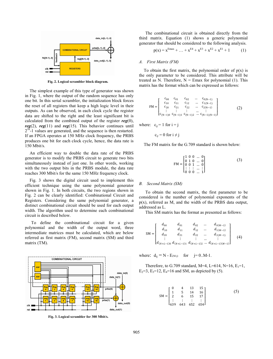
Fig. 2 depicts a general block diagram of a logical
scrambler. The architecture of this module implements a
register set which are feedback through a combinational
circuit [2][3].
The pseudorandom signal generated by the circuit feed
the output bus called prbs[(L-1)..0], where L represents the
number of output bits.
Fig. 1. G.709 Serial scrambler block diagram [1].
978-1-4673-2527-1/12/$31.00 ©2012 IEEE
904
�
The combinational circuit is obtained directly from the
third matrix. Equation (1) shows a generic polynomial
generator that should be considered to the following analysis.
p(x) = xEmax + … + xE4 + xE3 + xE2 + xE1 + 1 (1)
A. First Matrix (FM)
To obtain the first matrix, the polynomial order of p(x) is
the only parameter to be considered. This attribute will be
treated as N. Therefore, N = Emax for polynomial (1). This
matrix has the format which can be expressed as follows:
c00
c01
c02 … c0(N−1)
FM=
c(N−1)0c(N−1)1c(N−1)2 … c(N−1)(N−1)
c10
c11
c12 … c1(N−1)
c20
c21
c22 … c2(N−1)
⋮
⋮
⋮
… ⋮
(2)
where: cij = 1 for i = j
cij = 0 for i ≠ j
The FM matrix for the G.709 standard is shown below:
FM=10 0 … 0
00 0 … 1
01 0 … 0
00 1 … 0
⋮ ⋮ … ⋮
⋮
(3)
B. Second Matrix (SM)
To obtain the second matrix, the first parameter to be
considered is the number of polynomial exponents of the
p(x), referred as M, and the width of the PRBS data output,
addressed as L.
This SM matrix has the format as presented as follows:
01
11
00
02 … 0(−1)
SM=
(+−1)0(+−1)1(+−1)2 … (+−1)(−1)
12 … 1(−1)
10
20 21 22 … 2(−1)
⋮ ⋮ ⋮ … ⋮
(4)
where: dij = N - E(M-j) for j= 0..M-1.
Therefore, to G.709 standard, M=4, L=614, N=16, E1=1,
E2=3, E3=12, E4=16 and SM, as depicted by (5).
SM= 0
4
13
15
639 643 652 654
1
5
14
16
2
6
15
17
⋮
⋮
⋮
⋮
(5)
Fig. 2. Logical scrambler block diagram.
The simplest example of this type of generator was shown
in Fig. 1, where the output of the random sequence has only
one bit. In this serial scrambler, the initialization block forces
the reset of all registers that keep a high logic level in their
outputs. As can be observed, in each clock cycle the register
data are shifted to the right and the least significant bit is
calculated from the combined output of the register reg(0),
reg(2), reg(11) and reg(15). This behavior continues until
216-1 values are generated, and the sequence is then restarted.
If an FPGA operates at 150 MHz clock frequency, the PRBS
produces one bit for each clock cycle, hence, the data rate is
150 Mbit/s.
An efficient way to double the data rate of the PRBS
generator is to modify the PRBS circuit to generate two bits
simultaneously instead of just one. In other words, working
with the two output bits in the PRBS module, the data rate
reaches 300 Mbit/s for the same 150 MHz frequency clock.
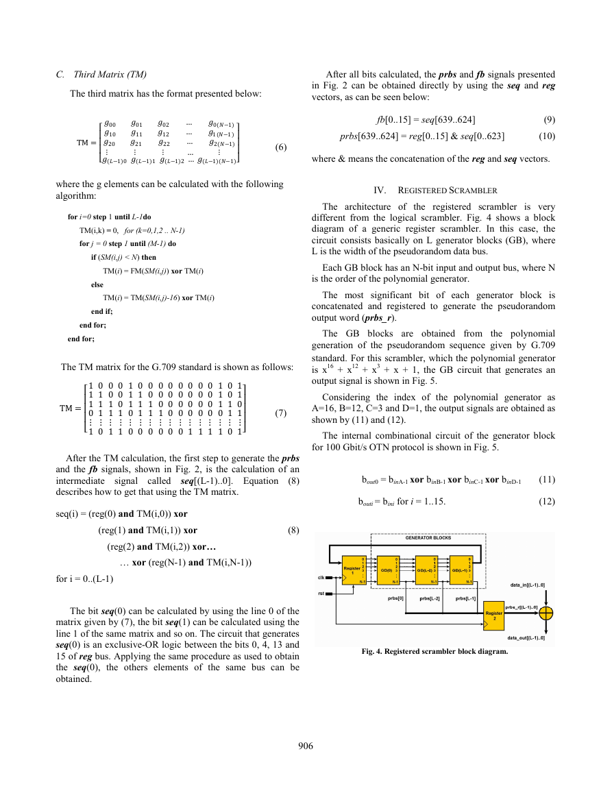
Fig. 3 shows the digital circuit used to implement this
efficient technique using the same polynomial generator
shown in Fig. 1. In both circuits, the two regions shown in
Fig. 2 can be clearly identified: Combinational Circuit and
Registers. Considering the same polynomial generator, a
distinct combinational circuit should be used for each output
width. The algorithm used to determine each combinational
circuit is described below.
To define
the combinational circuit
for a given
polynomial and
three
intermediate matrices must be calculated, which are below
referred as first matrix (FM), second matrix (SM) and third
matrix (TM).
the output word,
the width of
Fig. 3. Logical scrambler for 300 Mbit/s.
905
�
C. Third Matrix (TM)
The third matrix has the format presented below:
TM=00 01 02 … 0(−1)
(−1)0 (−1)1 (−1)2… (−1)(−1)
10 11 12 … 1(−1)
20 21 22 … 2(−1)
⋮ ⋮ ⋮ … ⋮
(6)
where the g elements can be calculated with the following
algorithm:
for i=0 step 1 until L-1do
TM(i,k) = 0, for (k=0,1,2 .. N-1)
for j = 0 step 1 until (M-1) do
if (SM(i,j) < N) then
TM(i) = FM(SM(i,j)) xor TM(i)
else
TM(i) = TM(SM(i,j)-16) xor TM(i)
end if;
end for;
end for;
The TM matrix for the G.709 standard is shown as follows:
TM=1000100000000101
1011000000111101
1100110000000101
1110111000000110
0111011100000011
⋮
⋮
⋮
⋮
⋮
⋮
⋮
⋮
⋮
⋮
⋮
⋮
⋮
⋮
⋮
⋮
(7)
After the TM calculation, the first step to generate the prbs
and the fb signals, shown in Fig. 2, is the calculation of an
intermediate signal called seq[(L-1)..0]. Equation
(8)
describes how to get that using the TM matrix.
After all bits calculated, the prbs and fb signals presented
in Fig. 2 can be obtained directly by using the seq and reg
vectors, as can be seen below:
fb[0..15] = seq[639..624] (9)
prbs[639..624] = reg[0..15] & seq[0..623] (10)
where & means the concatenation of the reg and seq vectors.
IV. REGISTERED SCRAMBLER
The architecture of the registered scrambler is very
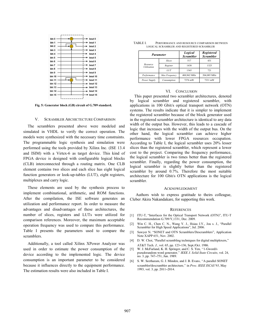
different from the logical scrambler. Fig. 4 shows a block
diagram of a generic register scrambler. In this case, the
circuit consists basically on L generator blocks (GB), where
L is the width of the pseudorandom data bus.
Each GB block has an N-bit input and output bus, where N
is the order of the polynomial generator.
The most significant bit of each generator block is
concatenated and registered to generate the pseudorandom
output word (prbs_r).
The GB blocks are obtained from
the polynomial
generation of the pseudorandom sequence given by G.709
standard. For this scrambler, which the polynomial generator
is x16 + x12 + x3 + x + 1, the GB circuit that generates an
output signal is shown in Fig. 5.
Considering the index of the polynomial generator as
A=16, B=12, C=3 and D=1, the output signals are obtained as
shown by (11) and (12).
The internal combinational circuit of the generator block
for 100 Gbit/s OTN protocol is shown in Fig. 5.
bout0 = binA-1 xor binB-1 xor binC-1 xor binD-1 (11)
bouti = bini for i = 1..15. (12)
seq(i) = (reg(0) and TM(i,0)) xor
(reg(1) and TM(i,1)) xor (8)
(reg(2) and TM(i,2)) xor…
… xor (reg(N-1) and TM(i,N-1))
for i = 0..(L-1)
The bit seq(0) can be calculated by using the line 0 of the
matrix given by (7), the bit seq(1) can be calculated using the
line 1 of the same matrix and so on. The circuit that generates
seq(0) is an exclusive-OR logic between the bits 0, 4, 13 and
15 of reg bus. Applying the same procedure as used to obtain
the seq(0), the others elements of the same bus can be
obtained.
Fig. 4. Registered scrambler block diagram.
906
�
Fig. 5: Generator block (GB) circuit of G.709 standard.
V. SCRAMBLER ARCHICTECTURE COMPARISON
The scramblers presented above were modeled and
simulated in VHDL to verify the correct operation. The
models were synthesized with the necessary time constraints.
The programmable logic synthesis and simulation were
performed using the tools provided by Xilinx Inc. (ISE 13.4
and ISIM) with a Virtex-6 as target device. This kind of
FPGA device is designed with configurable logical blocks
(CLB) interconnected through a routing matrix. One CLB
element contains two slices and each slice has eight logical
function generators or look-up-tables (LUT), eight registers,
multiplexes and carry logic.
the compilation,
These elements are used by the synthesis process to
implement combinational, arithmetic, and ROM functions.
After
the ISE software generates an
utilization and performance report. In order to measure the
advantages and disadvantages of these architectures, the
number of slices, registers and LUTs were utilized for
comparison references. Moreover, the maximum acceptable
operation frequency was used to compare this performance.
Table I presents the parameters used to compare the
scramblers.
Additionally, a tool called Xilinx XPower Analyzer was
used in order to estimate the power consumption of the
device according to the implemented logic. The device
consumption is an important parameter to be considered
because it influences directly to the equipment performance.
The estimation results were also included in Table I.
TABLE I.
PERFORMANCE AND RESOURCE COMPARISON BETWEEN
LOGICAL SCRAMBLER AND REGISTERED SCRAMBLER
Registered
Scrambler
Scrambler
Parameter
Logical
Resource
Utilization
Slices
Register
LUT
517
1430
1365
431
1325
721
Performance
Power Supply
Max Frequency
Consumption
400,962 MHz
204,085 MHz
7276 mW
7331 mW
VI. CONCLUSION
the
logical scrambler and
This paper presented two scrambler architectures, denoted
registered scrambler, with
by
applications in 100 Gbit/s optical transport network (OTN)
systems. The results indicate that it is simpler to implement
the registered scrambler because of the block generator used
in the registered scrambler architecture is identical to any data
width of the output bus. However, this leads to a cascade of
logic that increases with the width of the output bus. On the
logical scrambler can achieve higher
other hand,
performance with
resources occupation.
According to Table I, the logical scrambler uses 20% lesser
slices than the registered scrambler, which represent a lower
cost to the project. Comparing the frequency performance,
the logical scrambler is two times better than the registered
scrambler. Finally, regarding the power consumption, the
logical scrambler is slightly better than the registered
scrambler by around 0.7%. Therefore the most suitable
architecture for 100 Gbit/s OTN applications is the logical
scrambler.
lower FPGA
ACKNOWLEDGMENT
Authors wish to express gratitude to theirs colleague,
Cleber Akira Nakandakare, for supporting this work.
REFERENCES
[1]
ITU-T, “Interfaces for the Optical Transport Network (OTN)”, ITU-T
Recommendation G.709/Y,1331, Dec. 2009.
[2] Win C. H., Chen C. N., Wang Y. J., Hsiau J.Y., Jou s. J., “Parallel
Scrambler for High Speed Applications”, Jul. 2006.
[3] Sawyer N. “SONET and OTN Scramblers/Descramblers”, Application
Note XAPP 651, Nov. 2002.
[4] D. W. Choi, “Parallel scrambling techniques for digital multiplexers,”
AT&T Tech. J., vol. 65, pp. 123---136, Sept./Oct. 1986.
[5] W. J. McFarland, K. H. Springer, and C. S. Yen, ‘‘1-Gword/s
pseudorandom word generator,’’ IEEE J. Solid-State Circuits, vol. 24,
no. 3, pp. 747---751, Jun. 1989.
[6] S. W. Seetharam, G. J. Minden, and J. B. Evans, ‘‘A parallel SONET
scrambler/descrambler architecture,’’ in Proc. IEEE ISCAS’93, May
1993, vol. 3, pp. 2011---2014.
907
�


 2023年江西萍乡中考道德与法治真题及答案.doc
 2012年重庆南川中考生物真题及答案.doc
 2013年江西师范大学地理学综合及文艺理论基础考研真题.doc
 2020年四川甘孜小升初语文真题及答案I卷.doc
 2020年注册岩土工程师专业基础考试真题及答案.doc
 2023-2024学年福建省厦门市九年级上学期数学月考试题及答案.doc
 2021-2022学年辽宁省沈阳市大东区九年级上学期语文期末试题及答案.doc
 2022-2023学年北京东城区初三第一学期物理期末试卷及答案.doc
 2018上半年江西教师资格初中地理学科知识与教学能力真题及答案.doc
 2012年河北国家公务员申论考试真题及答案-省级.doc
 2020-2021学年江苏省扬州市江都区邵樊片九年级上学期数学第一次质量检测试题及答案.doc
 2022下半年黑龙江教师资格证中学综合素质真题及答案.doc