JEDEC
STANDARD
Serial Interface for Data Converters
JESD204B
(Revision of JESD204A, April 2008)
JULY 2011
JEDEC SOLID STATE TECHNOLOGY ASSOCIATION
�
NOTICE
JEDEC standards and publications contain material that has been prepared, reviewed, and
approved through the JEDEC Board of Directors level and subsequently reviewed and approved
by the JEDEC legal counsel.
JEDEC standards and publications are designed to serve the public interest through eliminating
misunderstandings between manufacturers and purchasers, facilitating interchangeability and
improvement of products, and assisting the purchaser in selecting and obtaining with minimum
delay the proper product for use by those other than JEDEC members, whether the standard is to
be used either domestically or internationally.
JEDEC standards and publications are adopted without regard to whether or not their adoption
may involve patents or articles, materials, or processes. By such action JEDEC does not assume
any liability to any patent owner, nor does it assume any obligation whatever to parties adopting
the JEDEC standards or publications.
The information included in JEDEC standards and publications represents a sound approach to
product specification and application, principally from the solid state device manufacturer
viewpoint. Within the JEDEC organization there are procedures whereby a JEDEC standard or
publication may be further processed and ultimately become an ANSI standard.
No claims to be in conformance with this standard may be made unless all requirements stated in
the standard are met.
Inquiries, comments, and suggestions relative to the content of this JEDEC standard or
publication should be addressed to JEDEC at the address below, or refer to www.jedec.org under
Standards and Documents for alternative contact information.
©JEDEC Solid State Technology Association 2011
Published by
3103 North 10th Street
Suite 240 South
Arlington, VA 22201-2107
This document may be downloaded free of charge; however JEDEC retains the
copyright on this material. By downloading this file the individual agrees not to
charge for or resell the resulting material.
PRICE: Contact JEDEC
Printed in the U.S.A.
All rights reserved
�
PLEASE!
DON’T VIOLATE
THE
LAW!
This document is copyrighted by JEDEC and may not be
reproduced without permission.
Organizations may obtain permission to reproduce a limited number of copies
through entering into a license agreement. For information, contact:
JEDEC Solid State Technology Association
3103 North 10th Street
Suite 240 South
Arlington, VA 22201-2107
or refer to www.jedec.org under Standards and Documents
for alternative contact information.
�
�
SERIAL INTERFACE FOR DATA CONVERTERS
Scope
(From JEDEC Board Ballot JCB-08-01 and JCB-11-47, formulated under the cognizance of JC-16
Committee on Interface Technology.)
1
This specification describes a serialized interface between data converters and logic devices. It contains
normative information to enable designers to implement devices that communicate with other devices
covered by this specification. Informative annexes are included to clarify and exemplify the specification.
Due to the range of applications involved, the intention of the document is to completely specify only the
serial data interface and the link protocol. Certain signals common to both the interface and the function
of the device, such as device clocks and control interfaces, have application-dependent requirements.
Devices may also have application-dependent modes, such as a low power / shutdown mode that will
affect the interface. In these instances, the specification merely constrains other device properties as they
relate to the interface, and leaves the specific implementation up to the designer.
Revision A of the standard was expanded to support serial data interfaces consisting of single or multiple
lanes per converter device. In addition, converter functionality (ADC or DAC) can be distributed over
multiple devices:
• All parallel running devices are implemented or specified to run synchronously with each other using
JEDEC Standard No. 204B
Page 1
the same data format.
• Normally this means that they are part of the same product family.
Revision B of the standard now supports the following additional functions:
• Mechanism for achieving repeatable, programmable deterministic delay across the JESD204 link.
• Support for serial data rates up to 12.5 Gbps.
• Transition from using frame clock as the main clock source to using device clock as the main clock
source. Device clock frequency requirements offer much more flexibility compared to requiring a
frame clock input.
The logic device (e.g. ASIC or FPGA) is always assumed to be a single device.
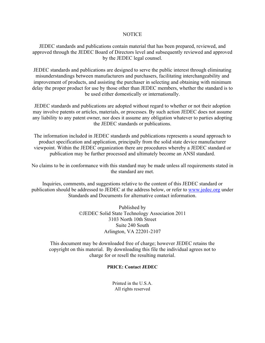
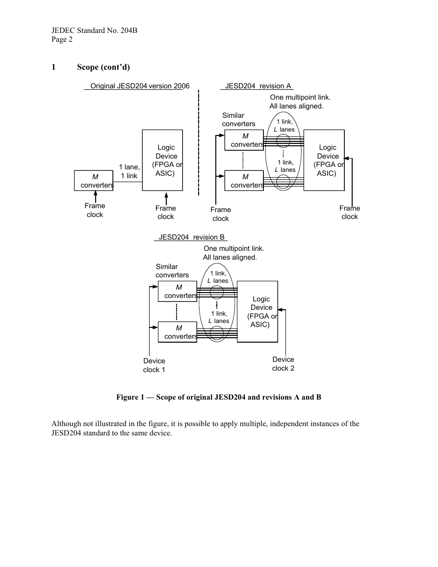
Figure 1 compares the scope of the original JESD204 specification and its revisions.
�
JEDEC Standard No. 204B
Page 2
1
Scope (cont’d)
Original JESD204 version 2006
Logic
Device
(FPGA or
ASIC)
1 lane,
1 link
M
converters
Frame
clock
JESD204 revision A
One multipoint link.
All lanes aligned.
1 link,
L lanes
1 link,
L lanes
Logic
Device
(FPGA or
ASIC)
Similar
converters
M
converters
M
converters
Frame
clock
Frame
clock
JESD204 revision B
Frame
clock
Similar
converters
M
converters
M
converters
Device
clock 1
One multipoint link.
All lanes aligned.
1 link,
L lanes
1 link,
L lanes
Logic
Device
(FPGA or
ASIC)
Device
clock 2
Figure 1 — Scope of original JESD204 and revisions A and B
Although not illustrated in the figure, it is possible to apply multiple, independent instances of the
JESD204 standard to the same device.
�
JEDEC Standard No. 204B
Page 3
Normative
References
2
2.1
The following normative documents contain provisions that, through reference in this text, constitute
provisions of this standard. For dated references, subsequent amendments to, or revisions of, any of these
publications do not apply. However, parties to agreements based on this standard are encouraged to
investigate the possibility of applying the most recent editions of the normative documents indicated
below. For undated references, the latest edition of the normative document referred to applies.
1. IEEE Std 802.3-2008®, Part 3, Section Three, Local and metropolitan area networks - CSMA/CD
access methods and Physical Layer specifications, 2008. http://standards.ieee.org/getieee802/
2. JEDEC JESD99, Terms, Definitions, and Letter Symbols for Microelectronic Devices.
3. OIF-SxI-5-01.0, System Interface Level 5 (SxI-5): Common Electrical Characteristics for 2.488 –
3.125Gbps Parallel Interfaces, Optical Internetworking Forum, October 2002.
www.oiforum.com/public/documents/OIF-SxI5-01.0.pdf
4. OIF-CEI-02.0, Common Electrical I/O- Electrical and Jitter Interoperability agreements for 6G+ bps
and 11G+ bps I/O, Optical Internetworking Forum, February 2005.
www.oiforum.com/public/documents/OIF_CEI_02.0.pdf
Informative
2.2
The following standards contain provisions that, through references in the text, are informative in this
standard.
5. ANSI T1.523-2001, ATIS Telecom Glossary 2000, February 2001. http://www.atis.org/tg2k/
6. IEEE Std 802.3-2008®, Part 3, Section Four, Local and metropolitan area networks - CSMA/CD
access methods and Physical Layer specifications, 2008. http://standards.ieee.org/getieee802/
7. ANSI/IEEE Std 91a-1991, Graphic symbols for logic functions, IEEE 1991, ANSI 1994. (Summary
available at e.g. http://en.wikipedia.org/wiki/Logic_gate)
8. INCITS 450-2009, Information technology - Fibre Channel - Physical Interface - 4 (FC-PI-4),
available from http://webstore.ansi.org
9. INCITS TR-35-2004 (R2009), Fibre Channel - Methodologies for Jitter and Signal Quality
Specification (FC-MJSQ) , available from http://webstore.ansi.org
�
Terminology
Terms and definitions
JEDEC Standard No. 204B
Page 4
3
For the purposes of this standard, the terms and definitions given in JESD99 (reference 2) and the
following apply:
3.1
8B/10B code: A DC-balanced octet-oriented data encoding specified in reference 1, clause 36.2.4. (Ref.
IEEE 802.3)
ceil(x): The smallest integer greater than or equal to x.
character: A symbol produced by 8B/10B encoding of an octet.
NOTE 1 While all octets can be encoded as data characters, certain octets can also be encoded as control
characters.
NOTE 2 The same character may exist as two different code groups, depending on running disparity.
character clock: A signal used for sequencing the 8B/10B characters or octets.
clock generator: A circuit used to generate synchronous, phase aligned device clocks to various devices
in the JESD204B system.
NOTE A clock generator circuit can include one or more clock generator devices, but they must use a common
source clock.
code group: A set of ten bits that, when representing data, conveys an octet. (Ref. IEEE 802.3)
control interface: An application-specific interface used to pass information (usually status and control
information) between a converter device and a logic device and/or between a device and a higher layer
application level.
NOTE The details of the control interface are outside the scope of the serial interface described by this standard.
conversion clock: A signal used to define the analog sampling moments in a converter.
NOTE Usually the conversion clock is the same as the sample clock, except in case of interpolating DACs or
decimating ADCs, where the conversion clock is faster than the sample clock. In all cases, the conversion clock is
derived from the device clock.
converter: An analog-to-digital converter (ADC) or digital-to-analog converter (DAC).
NOTE
converter device: A component package containing one or more converters.
NOTE This standard specifies the interactions between one logic device and one or more converter devices.
In this standard, a converter is assumed to interface via a single stream of digital samples.
�



 2023年江西萍乡中考道德与法治真题及答案.doc
 2012年重庆南川中考生物真题及答案.doc
 2013年江西师范大学地理学综合及文艺理论基础考研真题.doc
 2020年四川甘孜小升初语文真题及答案I卷.doc
 2020年注册岩土工程师专业基础考试真题及答案.doc
 2023-2024学年福建省厦门市九年级上学期数学月考试题及答案.doc
 2021-2022学年辽宁省沈阳市大东区九年级上学期语文期末试题及答案.doc
 2022-2023学年北京东城区初三第一学期物理期末试卷及答案.doc
 2018上半年江西教师资格初中地理学科知识与教学能力真题及答案.doc
 2012年河北国家公务员申论考试真题及答案-省级.doc
 2020-2021学年江苏省扬州市江都区邵樊片九年级上学期数学第一次质量检测试题及答案.doc
 2022下半年黑龙江教师资格证中学综合素质真题及答案.doc