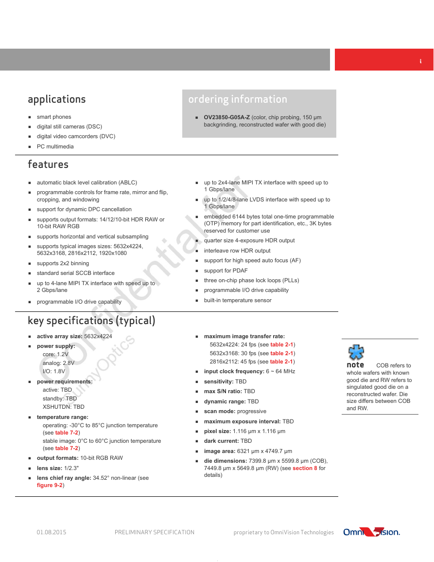
applications
features
key specifications (typical)
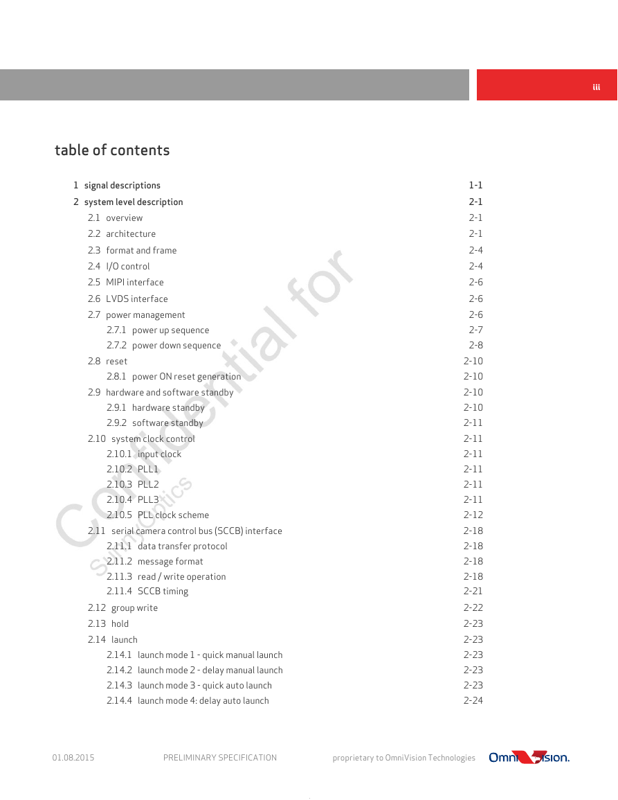
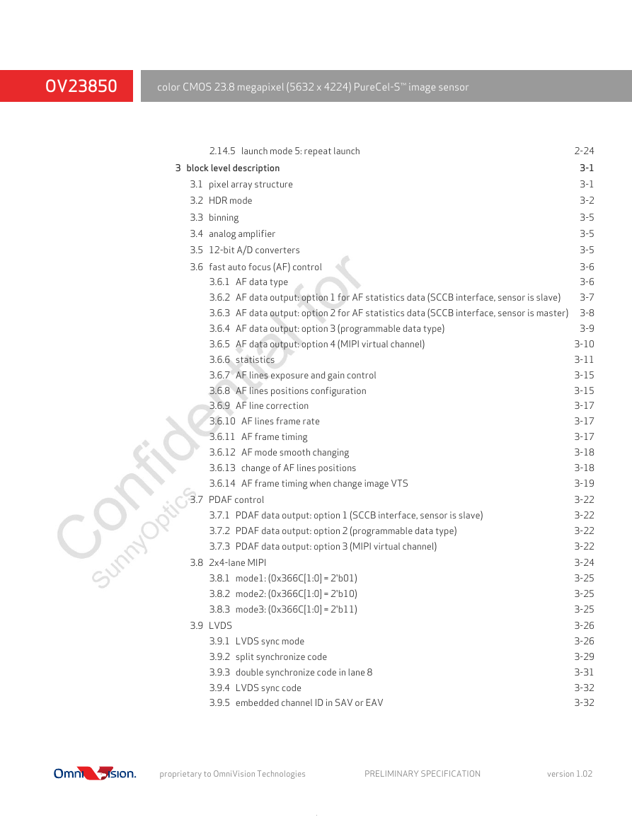
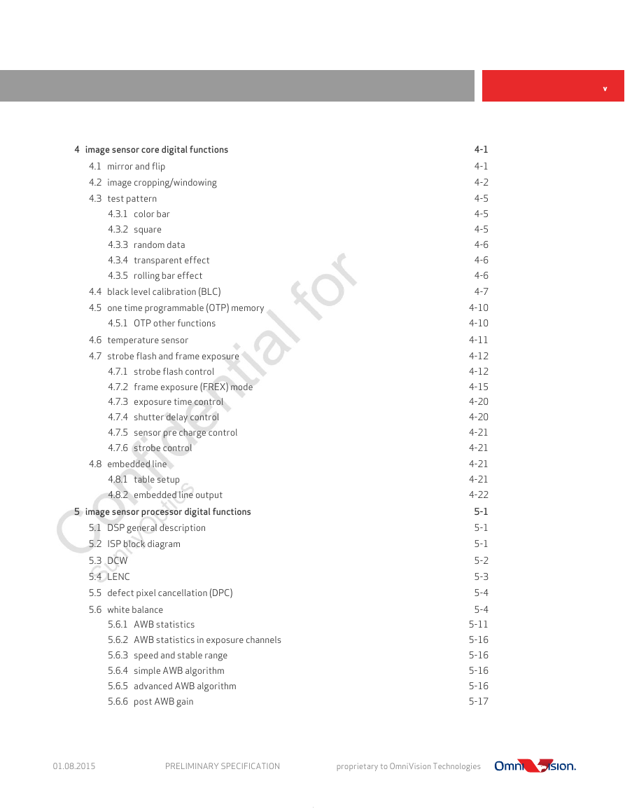
table of contents
list of figures
list of tables
1 signal descriptions
table 1-1 signal descriptions (sheet 1 of 5)
table 1-2 configuration under various conditions (sheet 1 of 3)
figure 1-1 pad diagram
table 1-3 pad symbol and equivalent circuit (sheet 1 of 2)
2 system level description
2.1 overview
2.2 architecture
figure 2-1 OV23850 block diagram
figure 2-2 OV23850 reference design schematic
2.3 format and frame
table 2-1 format and frame rate
2.4 I/O control
table 2-2 I/O control registers (sheet 1 of 3)
2.5 MIPI interface
2.6 LVDS interface
2.7 power management
2.7.1 power up sequence
table 2-3 power up sequence timing constraints
figure 2-3 power up sequence
2.7.2 power down sequence
table 2-4 power down sequence timing constraints
figure 2-4 software standby sequence
figure 2-5 power down sequence
2.8 reset
2.8.1 power ON reset generation
2.9 hardware and software standby
2.9.1 hardware standby
2.9.2 software standby
table 2-5 hardware and standby description
2.10 system clock control
2.10.1 input clock
2.10.2 PLL1
2.10.3 PLL2
2.10.4 PLL3
2.10.5 PLL clock scheme
figure 2-6 clock scheme diagram
table 2-6 PLL control registers (sheet 1 of 6)
2.11 serial camera control bus (SCCB) interface
2.11.1 data transfer protocol
2.11.2 message format
figure 2-7 message type
2.11.3 read / write operation
figure 2-8 SCCB single read from random location
figure 2-9 SCCB single read from current location
figure 2-10 SCCB sequential read from random location
figure 2-11 SCCB sequential read from current location
figure 2-12 SCCB single write to random location
figure 2-13 SCCB sequential write to random location
2.11.4 SCCB timing
figure 2-14 SCCB interface timing
table 2-7 SCCB interface timing specifications
2.12 group write
table 2-8 context switching control
2.13 hold
2.14 launch
2.14.1 launch mode 1 - quick manual launch
2.14.2 launch mode 2 - delay manual launch
2.14.3 launch mode 3 - quick auto launch
2.14.4 launch mode 4: delay auto launch
2.14.5 launch mode 5: repeat launch
3 block level description
3.1 pixel array structure
figure 3-1 sensor array region color filter layout
3.2 HDR mode
figure 3-2 2-exposure HDR diagram
table 3-1 2-exposure HDR control registers (sheet 1 of 2)
figure 3-3 4-exposure HDR diagram
table 3-2 4-exposure HDR control registers (sheet 1 of 2)
3.3 binning
figure 3-4 example of 2x2 binning
table 3-3 binning-related registers
3.4 analog amplifier
3.5 12-bit A/D converters
3.6 fast auto focus (AF) control
figure 3-5 AF line in image area diagram
3.6.1 AF data type
3.6.2 AF data output: option 1 for AF statistics data (SCCB interface, sensor is slave)
figure 3-6 option 1 for AF statistics data
figure 3-7 SCCB sequential read from random location
3.6.3 AF data output: option 2 for AF statistics data (SCCB interface, sensor is master)
table 3-4 AF SCCB control registers
figure 3-8 option 2 for AF statistics data
3.6.4 AF data output: option 3 (programmable data type)
figure 3-9 option 3 for AF statistics data
3.6.5 AF data output: option 4 (MIPI virtual channel)
figure 3-10 option 4 for AF statistics data
3.6.6 statistics
figure 3-11 AFC windows
figure 3-12 AF windows histogram lists
table 3-5 AFC statistics control registers
table 3-6 auto focus statistic read only registers (sheet 1 of 4)
3.6.7 AF lines exposure and gain control
3.6.8 AF lines positions configuration
figure 3-13 AF position configuration diagram
3.6.9 AF line correction
3.6.10 AF lines frame rate
3.6.11 AF frame timing
figure 3-14 AF frame output timing diagram
3.6.12 AF mode smooth changing
figure 3-15 AF smooth change diagram
3.6.13 change of AF lines positions
figure 3-16 change of AF lines positions diagram
3.6.14 AF frame timing when change image VTS
figure 3-17 VTS change in auto-interval mode
figure 3-18 VTS change in fixed interval mode
table 3-7 auto focus control registers (sheet 1 of 3)
3.7 PDAF control
3.7.1 PDAF data output: option 1 (SCCB interface, sensor is slave)
3.7.2 PDAF data output: option 2 (programmable data type)
3.7.3 PDAF data output: option 3 (MIPI virtual channel)
figure 3-19 PDAF data output diagram
table 3-8 PDAF control registers (sheet 1 of 2)
3.8 2x4-lane MIPI
figure 3-20 2x4-lane MIPI diagram
3.8.1 mode1: (0x366C[1:0] = 2'b01)
figure 3-21 mode 1 diagram
3.8.2 mode2: (0x366C[1:0] = 2'b10)
figure 3-22 mode 2 diagram
3.8.3 mode3: (0x366C[1:0] = 2'b11)
figure 3-23 mode 3 diagram
table 3-9 2x4 lane MIPI control registers
3.9 LVDS
3.9.1 LVDS sync mode
figure 3-24 LVDS 1-lane mode
figure 3-25 LVDS 2-lane mode (sync code option 2)
figure 3-26 LVDS 4-lane mode (sync code option 2)
figure 3-27 LVDS 8-lane mode (sync code option 2)
3.9.2 split synchronize code
figure 3-28 LVDS 1-lane mode
figure 3-29 LVDS 2-lane mode (sync code option 1)
figure 3-30 LVDS 4-lane mode (sync code option 1)
figure 3-31 LVDS 8-lane mode (sync code option 1)
3.9.3 double synchronize code in lane 8
figure 3-32 LVDS 8-lane mode (sync code option 3)
3.9.4 LVDS sync code
table 3-10 10-bit sync code
table 3-11 12-bit sync code
3.9.5 embedded channel ID in SAV or EAV
table 3-12 LVDS control registers
4 image sensor core digital functions
4.1 mirror and flip
figure 4-1 mirror and flip samples
table 4-1 mirror and flip registers
4.2 image cropping/windowing
figure 4-2 image cropping/windowing
table 4-2 image cropping/windowing control functions (sheet 1 of 2)
4.3 test pattern
4.3.1 color bar
figure 4-3 color bar types
4.3.2 square
figure 4-4 color, black and white square bars
4.3.3 random data
4.3.4 transparent effect
figure 4-5 transparent effect
4.3.5 rolling bar effect
figure 4-6 rolling bar effect
table 4-3 test pattern registers
4.4 black level calibration (BLC)
table 4-4 BLC control registers (sheet 1 of 2)
4.5 one time programmable (OTP) memory
4.5.1 OTP other functions
table 4-5 OTP control registers (sheet 1 of 2)
4.6 temperature sensor
table 4-6 temperature sensor functions
4.7 strobe flash and frame exposure
4.7.1 strobe flash control
figure 4-7 xenon flash mode
figure 4-8 LED 1 & 2 mode - one pulse output
figure 4-9 LED 1 & 2 mode - multiple pulse output
figure 4-10 LED 3 mode
figure 4-11 LED 4 mode
4.7.2 frame exposure (FREX) mode
figure 4-12 FREX mode 1
figure 4-13 FREX mode 2
figure 4-14 FREX mode 1 timing diagram
figure 4-15 FREX mode 2 (shutter delay = 0) timing diagram
figure 4-16 FREX mode 2 (shutter delay > 0) timing diagram
table 4-7 flash strobe control registers
table 4-8 FREX strobe control registers (sheet 1 of 2)
4.7.3 exposure time control
4.7.4 shutter delay control
4.7.5 sensor pre charge control
4.7.6 strobe control
4.8 embedded line
4.8.1 table setup
4.8.2 embedded line output
table 4-9 embedded line registers (sheet 1 of 2)
5 image sensor processor digital functions
5.1 DSP general description
figure 5-1 typical pixel layout for 4-exposure 4x4 diagram
5.2 ISP block diagram
figure 5-2 ISP block diagram
5.3 DCW
5.4 LENC
figure 5-3 lens correction graph
table 5-1 lens correction registers (sheet 1 of 2)
5.5 defect pixel cancellation (DPC)
5.6 white balance
table 5-2 gain and offset chart
table 5-3 MWB control registers (sheet 1 of 6)
5.6.1 AWB statistics
figure 5-4 advanced AWB diagram
figure 5-5 AWB ROI position diagram
table 5-4 weight map
table 5-5 curve based AWB registers (sheet 1 of 3)
5.6.2 AWB statistics in exposure channels
5.6.3 speed and stable range
table 5-6 AWB stable range registers
5.6.4 simple AWB algorithm
5.6.5 advanced AWB algorithm
5.6.6 post AWB gain
table 5-7 combine RISC registers
5.7 CIP
figure 5-6 typical pixel layout for 4-exposure 4x4 diagram
5.7.1 CIP as a general color interpolation module
5.7.2 CIP as a binning correction filter
figure 5-7 CIP binning correction filter diagram
5.7.3 binning correction in horizontal direction
figure 5-8 binning correction in horizontal direction diagram
5.8 AEC/AGC algorithm
5.8.1 position weight
figure 5-9 AEC/AGC statistics window diagram
table 5-8 AEC/AGC control registers (sheet 1 of 3)
5.8.2 adaptive weight (combination weight)
5.8.3 luminance weight
table 5-9 exposure time and gain registers
table 5-10 AEC control registers (sheet 1 of 2)
5.8.4 manual exposure mode
5.9 combine
5.9.1 2D combination
figure 5-10 2D combination diagram
5.9.2 1D combination
figure 5-11 1D combination diagram
table 5-11 combine/tonemap registers (sheet 1 of 4)
5.10 tone mapping
table 5-12 tonemap register
figure 5-12 4x4 window array diagram
figure 5-13 tone curve
figure 5-14 local tone mapping diagram
table 5-13 combine RISC register
5.11 raw_DNS
table 5-14 RAW_DNS registers (sheet 1 of 2)
5.12 fast_DNS
5.13 PDC
table 5-15 PDC registers (sheet 1 of 2)
5.14 window
6 register tables
6.1 PLL control [0x0300 ~ 0x0321, 0x0328 ~ 0x032B]
table 6-1 PLL control registers (sheet 1 of 6)
6.2 system control [0x3000 ~ 0x302A, 0x302C, 0x3031 ~ 0x303F, 0x3660 ~ 0x366C]
table 6-2 system control registers (sheet 1 of 9)
6.3 SCCB control [0xFFF0 ~ 0xFFFC]
table 6-3 SCCB control registers
6.4 group hold [0x3200 ~ 0x320F]
table 6-4 group hold registers (sheet 1 of 3)
6.5 power saving control [0x3400 ~ 0x340A, 0x340C ~ 0x340D]
table 6-5 power saving control registers (sheet 1 of 2)
6.6 sensor timing control [0x3700 ~ 0x37C9, 0x4B01, 0x4B03, 0x4B06 ~ 0x4B0B, 0x4B10]
table 6-6 sensor timing control registers (sheet 1 of 4)
6.7 timing control [0x3800 ~ 0x3845, 0x3850 ~ 0x3858, 0x3860 ~ 0x3863]
table 6-7 timing control registers (sheet 1 of 6)
6.8 embedded line [0x3666, 0x3900 ~ 0x3903, 0x3906 ~ 0x3907, 0x5C08]
table 6-8 embedded line registers (sheet 1 of 2)
6.9 strobe control [0x3B00, 0x3B02 ~ 0x3B05]
table 6-9 strobe control registers (sheet 1 of 2)
6.10 illumination PWM [0x3B40 ~ 0x3B52]
table 6-10 illumination PWM registers (sheet 1 of 3)
6.11 OTP control [0x3D80 ~ 0x3D8D, 0x3D90, 0x6000 ~ 0x77FF]
table 6-11 OTP control registers (sheet 1 of 3)
6.12 FREX control [0x3F85 ~ 0x3F87, 0x3F89 ~ 0x3F93, 0x3F9E ~ 0x3F9F]
table 6-12 FREX strobe control registers (sheet 1 of 2)
6.13 BLC control [0x4000 ~ 0x401A, 0x4020 ~ 0x406D, 0x4070 ~ 0x40BF]
table 6-13 BLC control registers (sheet 1 of 11)
6.14 frame control [0x4200 ~ 0x4203]
table 6-14 frame control registers (sheet 1 of 2)
6.15 ISP frame counter [0x4900 ~ 0x4903]
table 6-15 ISP frame counter control registers
6.16 VFIFO control [0x4600 ~ 0x4605]
table 6-16 VFIFO control registers
6.17 PDFIFO control [0x4640 ~ 0x4645]
table 6-17 PDFIFO control registers (sheet 1 of 2)
6.18 LVDS control [0x4700, 0x4702 ~ 0x470F]
table 6-18 LVDS control registers (sheet 1 of 2)
6.19 MIPI control [0x4800 ~ 0x4809, 0x4810 ~ 0x4833, 0x4836 ~ 0x48A1]
table 6-19 MIPI control registers (sheet 1 of 14)
6.20 temperature sensor [0x4D00 ~ 0x4D14]
table 6-20 temperature sensor registers (sheet 1 of 2)
6.21 AFC statistics control [0x4F00 ~ 0x4F1E, 0x4F20 ~ 0x4F24, 0x4F30 ~ 0x4F89]
table 6-21 AFC statistics control registers (sheet 1 of 6)
6.22 DSP control [0x5000 ~ 0x5079]
table 6-22 DSP control registers (sheet 1 of 7)
6.23 MEC/MGC [0x3500 ~ 0x3521, 0x3541 ~ 0x3548, 0x354A ~ 0x354B, 0x354E ~ 0x354F]
table 6-23 MEC/MGC control registers (sheet 1 of 4)
6.24 AEC/AGC control [0x5100 ~ 0x5170]
table 6-24 AEC/AGC control registers (sheet 1 of 7)
6.25 AEC_stat control [0x5400 ~ 0x5452]
table 6-25 AEC_stat control registers (sheet 1 of 3)
6.26 pre_ISP [0x5280 ~ 0x5292, 0x52A0 ~ 0x52B4, 0x52B6 ~ 0x52B9]
table 6-26 pre_ISP registers (sheet 1 of 4)
6.27 MWB gain control [0x5300 ~ 0x5316, 0x5320 ~ 0x5336, 0x5340 ~ 0x5383]
table 6-27 MWB gain control registers (sheet 1 of 7)
6.28 curve based AWB [0x5980 ~ 0x59BB]
table 6-28 curve based AWB registers (sheet 1 of 5)
6.29 curve AWB RISC [0x5E01, 0x5E03 ~ 0x5E07, 0x5F00 ~ 0x5F1B, 0x5F20 ~ 0x5F9B]
table 6-29 curve AWB RISC registers (sheet 1 of 6)
6.30 LENC control [0x2800 ~ 0x2B09, 0x2B10 ~ 0x2B16]
table 6-30 LENC control registers (sheet 1 of 2)
6.31 mapping control [0x5500 ~ 0x55FF]
table 6-31 mapping control registers (sheet 1 of 9)
6.32 PDC control [0x5D00 ~ 0x5D32, 0x5D34 ~ 0x5D39, 0x5D40 ~ 0x5D44]
table 6-32 PDC control registers (sheet 1 of 3)
6.33 DPC control [0x5600 ~ 0x561A, 0x5620 ~ 0x563A, 0x5640 ~ 0x56A5]
table 6-33 DPC control registers (sheet 1 of 12)
6.34 CIP control [0x5700 ~ 0x575C, 0x5760 ~ 0x5794]
table 6-34 CIP control registers (sheet 1 of 6)
6.35 combine [0x5900 ~ 0x5920]
table 6-35 combine registers (sheet 1 of 2)
6.36 tone mapping [0x5A00 ~ 0x5A9E, 0x5B00 ~ 0x5B75]
table 6-36 tone mapping control registers (sheet 1 of 11)
6.37 HDR combine RISC [0x5D80 ~ 0x5D8B, 0x5E80 ~ 0x5E86]
table 6-37 HDR combine RISC registers
6.38 RAW DNS [0x5940 ~ 0x594D, 0x5950 ~ 0x595D, 0x5960 ~ 0x597D]
table 6-38 RAW_DNS registers (sheet 1 of 3)
6.39 fast DNS [0x5B80 ~ 0x5BD8]
table 6-39 fast DNS registers (sheet 1 of 5)
6.40 window [0x5C00 ~ 0x5C0C, 0x5C80 ~ 0x5C8D, 0x5CA0 ~ 0x5CA6, 0x5C90 ~ 0x5C97]
table 6-40 window control registers (sheet 1 of 2)
6.41 FW control [0x8000 ~ 0x8313]
table 6-41 FW control registers (sheet 1 of 22)
7 operating specifications
7.1 absolute maximum ratings
table 7-1 absolute maximum ratings
7.2 functional temperature
table 7-2 functional temperature
7.3 DC characteristics
table 7-3 DC characteristics (-30°C < TJ < 85°C)
7.4 timing characteristics
table 7-4 timing characteristics
8 mechanical specifications
8.1 COB physical specifications
figure 8-1 COB die specifications
table 8-1 pad location coordinates (sheet 1 of 4)
8.2 reconstructed wafer (RW) physical specifications
table 8-2 RW physical dimensions
figure 8-2 OV23850 RW physical diagram
9 optical specifications
9.1 sensor array center
figure 9-1 sensor array center
9.2 lens chief ray angle (CRA)
figure 9-2 chief ray angle (CRA)
table 9-1 CRA versus image height plot (sheet 1 of 2)
appendix A handling of RW devices
A.1 ESD /EOS prevention
A.2 particles and cleanliness of environment
A.3 other requirements
revision history


 2023年江西萍乡中考道德与法治真题及答案.doc
 2012年重庆南川中考生物真题及答案.doc
 2013年江西师范大学地理学综合及文艺理论基础考研真题.doc
 2020年四川甘孜小升初语文真题及答案I卷.doc
 2020年注册岩土工程师专业基础考试真题及答案.doc
 2023-2024学年福建省厦门市九年级上学期数学月考试题及答案.doc
 2021-2022学年辽宁省沈阳市大东区九年级上学期语文期末试题及答案.doc
 2022-2023学年北京东城区初三第一学期物理期末试卷及答案.doc
 2018上半年江西教师资格初中地理学科知识与教学能力真题及答案.doc
 2012年河北国家公务员申论考试真题及答案-省级.doc
 2020-2021学年江苏省扬州市江都区邵樊片九年级上学期数学第一次质量检测试题及答案.doc
 2022下半年黑龙江教师资格证中学综合素质真题及答案.doc