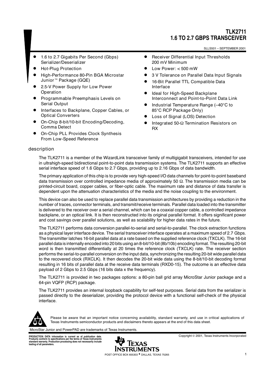
TLK27111.6 TO 2.7 GBPS TRANSCEIVERSLLS501 – SEPTEMBER 20011POST OFFICE BOX 655303 • DALLAS, TEXAS 75265D1.6 to 2.7 Gigabits Per Second (Gbps)Serializer/DeserializerDHot-Plug ProtectionDHigh-Performance 80-Pin BGA MicrostarJunior Package (GQE)D2.5-V Power Supply for Low PowerOperationDProgrammable Preemphasis Levels onSerial OutputDInterfaces to Backplane, Copper Cables, orOptical ConvertersDOn-Chip 8-bit/10-bit Encoding/Decoding,Comma DetectDOn-Chip PLL Provides Clock SynthesisFrom Low-Speed ReferenceDReceiver Differential Input Thresholds200 mV MinimumDLow Power: < 500 mWD3 V Tolerance on Parallel Data Input SignalsD16-Bit Parallel TTL Compatible DataInterfaceDIdeal for High-Speed BackplaneInterconnect and Point-to-Point Data LinkDIndustrial Temperature Range (–40°C to85°C RCP Package Only)DLoss of Signal (LOS) DetectionDIntegrated 50-Ω Termination Resistors onRX descriptionThe TLK2711 is a member of the WizardLink transceiver family of multigigabit transceivers, intended for usein ultrahigh-speed bidirectional point-to-point data transmission systems. The TLK2711 supports an effectiveserial interface speed of 1.6 Gbps to 2.7 Gbps, providing up to 2.16 Gbps of data bandwidth.The primary application of this chip is to provide very high-speed I/O data channels for point-to-point basebanddata transmission over controlled impedance media of approximately 50 Ω. The transmission media can beprinted-circuit board, copper cables, or fiber-optic cable. The maximum rate and distance of data transfer isdependent upon the attenuation characteristics of the media and the noise coupling to the environment.This device can also be used to replace parallel data transmission architectures by providing a reduction in thenumber of traces, connector terminals, and transmit/receive terminals. Parallel data loaded into the transmitteris delivered to the receiver over a serial channel, which can be a coaxial copper cable, a controlled impedancebackplane, or an optical link. It is then reconstructed into its original parallel format. It offers significant powerand cost savings over parallel solutions, as well as scalability for higher data rates in the future.The TLK2711 performs data conversion parallel-to-serial and serial-to-parallel. The clock extraction functionsas a physical layer interface device. The serial transceiver interface operates at a maximum speed of 2.7Gbps.The transmitter latches 16-bit parallel data at a rate based on the supplied reference clock (TXCLK). The 16-bitparallel data is internally encoded into 20 bits using an 8-bit/10-bit (8b/10b) encoding format. The resulting 20-bitword is then transmitted differentially at 20 times the reference clock (TXCLK) rate. The receiver sectionperforms the serial-to-parallel conversion on the input data, synchronizing the resulting 20-bit wide parallel datato the recovered clock (RXCLK). It then decodes the 20-bit wide data using the 8-bit/10-bit decoding formatresulting in 16 bits of parallel data at the receive data terminals (RXD0-15). The outcome is an effective datapayload of 2 Gbps to 2.5 Gbps (16 bits data x the frequency).The TLK2711 is provided in two packages options: a 80-pin ball grid array MicroStar Junior package and a64-pin VQFP (RCP) package.The TLK2711 provides an internal loopback capability for self-test purposes. Serial data from the serializer ispassed directly to the deserializer, providing the protocol device with a functional self-check of the physicalinterface.Please be aware that an important notice concerning availability, standard warranty, and use in critical applications ofTexasInstruments semiconductor products and disclaimers thereto appears at the end of this data sheet.Copyright 2001, Texas Instruments IncorporatedPRODUCTION DATA information is current as of publication date.Products conform to specifications per the terms of Texas Instrumentsstandard warranty. Production processing does not necessarily includetesting of all parameters.MicroStar Junior and PowerPAD are trademarks of Texas Instruments.�
TLK27111.6 TO 2.7 GBPS TRANSCEIVERSLLS501 – SEPTEMBER 20012POST OFFICE BOX 655303 • DALLAS, TEXAS 75265description (continued)The TLK2711 has a loss of signal (LOS) detection circuit for conditions where the incoming signal no longer hasa sufficient voltage amplitude to keep the clock recovery circuit in lock.The TLK2711 allows users to implement redundant ports by connecting receive data bus terminals from twoTLK2711 devices together. Asserting the LCKREFN to a low state will cause the receive data bus terminals,RXD[0:15], RXCLK, RKLSB, and RKMSB to go to a high-impedance state. This places the device in atransmit-only mode since the receiver is not tracking the data.The TLK2711 uses a 2.5-V supply. The I/O section is 3 V compatible. With the 2.5-V supply the chipset is verypower efficient, consuming less than 450 mW typically. The TLK2711 is characterized for operation from –40°Cto 85°C (RCP only).The TLK2711 is designed to be hot-plug capable. An on-chip power-on reset circuit holds the RXCLK low andgoes to high impedance on the parallel side output signal terminals as well as TXP and TXN during power up.�
TLK27111.6 TO 2.7 GBPS TRANSCEIVERSLLS501 – SEPTEMBER 20013POST OFFICE BOX 655303 • DALLAS, TEXAS 75265987654321987654321GNDTXD1TXPTXNPRERXPRXNRXD1GNDTXD3TXD2TXD0GNDAVDDAGNDARXD0RXD2RXD3TXD5TXD4VDDVDDVDDGNDGNDRXD4RXD5TXD6TXD7VDDVDDVDDGNDGNDRXD6RXD7TXCLKVDDVDDVDDVDDGNDGNDRXCLKRXD8TXD8TXD9VDDVDDVDDGNDGNDRXD11RXD9TXD10TXD11VDDVDDVDDGNDRXD12RXD10TXD12TXD13TKMSBLOOPENLCKREFNTESTENRKMSBRXD14RXD13GNDTXD14TXD15TKLSBENABLEPRBSENRKLSBRXD15GNDGQE PACKAGE(TOP VIEW)ABCDEFGHJ171819VDDRXD3RXD4RXD5RXD6GNDRXD7RX_CLKRXD8RXD9VDDRXD10RXD11RXD12RXD13GND484746454443424140393837363534332012345678910111213141516VDDTXD3TXD4TXD5GNDTXD6TXD7GTX_CLKVDDTXD8TXD9TXD10GNDTXD11TXD12TXD1321222324RXD1DINRXP63626160596458TXD0GNDADOUTTXPDOUTTXNGNDAPREPRBSENTESTENGNDRKLSBTXD15TKMSBLOOPENTKLSBDDENABLELCKREFN5655545725262728295352TXD14DINRXNGNDA515049303132RKMSBRXD15RXD14RXD0RXD2TXD2TXD1GNDRCP PACKAGE(TOP VIEW)VDDAVDDAV�
TLK27111.6 TO 2.7 GBPS TRANSCEIVERSLLS501 – SEPTEMBER 20014POST OFFICE BOX 655303 • DALLAS, TEXAS 75265block diagramLOOPENRXNRXPBIASPRERecoveredClockTXPTXNRXCLKRKMSBRKLSBTXD0–TXD1599RXDO–RXD15PRBSVerificationClockSynthesizerInterpolator andClock RecoveryENABLE10PRBSENTESTEN1010Controls:PLL,Bias,Rx,Tx8b/10bEncoder18 BitRegisterEncoder18 BitRegisterPRBSGeneratorMUXTXCLK2:1MUXParallel toSerial102:1MUX2:1MUXSerial toParallel101:2MUX1010992:1MUXDataCommaDetectand 8b/10bDecoding10CommaDetectand 8b/10bDecodingSignal Detect(LOS)TKLSBPRBSENTKMSBPRBSENPRBSENClock8b/10bFigure 1. TLK2711 Block Diagram�
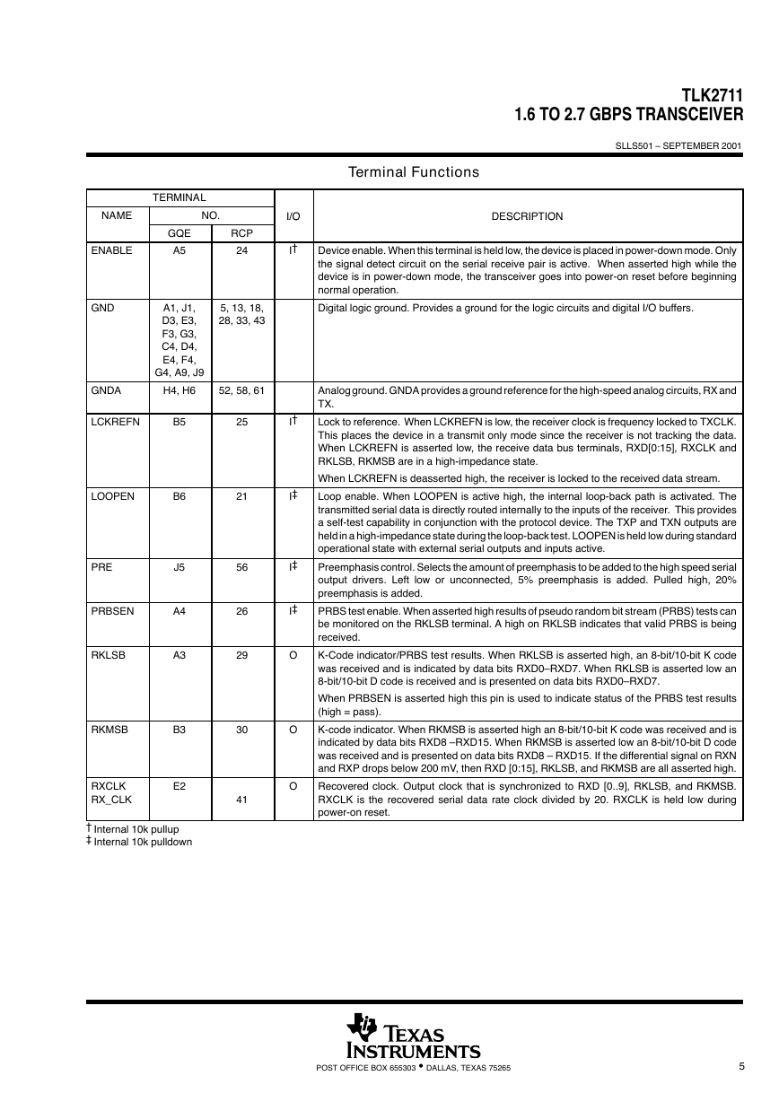
TLK27111.6 TO 2.7 GBPS TRANSCEIVERSLLS501 – SEPTEMBER 20015POST OFFICE BOX 655303 • DALLAS, TEXAS 75265Terminal FunctionsTERMINALNAMENO.I/ODESCRIPTIONGQERCPI/ODESCRIPTIONENABLEA524I†Device enable. When this terminal is held low, the device is placed in power-down mode. Onlythe signal detect circuit on the serial receive pair is active. When asserted high while thedevice is in power-down mode, the transceiver goes into power-on reset before beginningnormal operation.GNDA1, J1,D3, E3,F3, G3,C4, D4,E4, F4,G4, A9, J95, 13, 18,28, 33, 43Digital logic ground. Provides a ground for the logic circuits and digital I/O buffers.GNDAH4, H652, 58, 61Analog ground. GNDA provides a ground reference for the high-speed analog circuits, RX andTX.LCKREFNB525I†Lock to reference. When LCKREFN is low, the receiver clock is frequency locked to TXCLK.This places the device in a transmit only mode since the receiver is not tracking the data.When LCKREFN is asserted low, the receive data bus terminals, RXD[0:15], RXCLK andRKLSB, RKMSB are in a high-impedance state.When LCKREFN is deasserted high, the receiver is locked to the received data stream.LOOPENB621I‡Loop enable. When LOOPEN is active high, the internal loop-back path is activated. Thetransmitted serial data is directly routed internally to the inputs of the receiver. This providesa self-test capability in conjunction with the protocol device. The TXP and TXN outputs areheld in a high-impedance state during the loop-back test. LOOPEN is held low during standardoperational state with external serial outputs and inputs active.PREJ556I‡Preemphasis control. Selects the amount of preemphasis to be added to the high speed serialoutput drivers. Left low or unconnected, 5% preemphasis is added. Pulled high, 20%preemphasis is added.PRBSENA426I‡PRBS test enable. When asserted high results of pseudo random bit stream (PRBS) tests canbe monitored on the RKLSB terminal. A high on RKLSB indicates that valid PRBS is beingreceived.RKLSBA329OK-Code indicator/PRBS test results. When RKLSB is asserted high, an 8-bit/10-bit K codewas received and is indicated by data bits RXD0–RXD7. When RKLSB is asserted low an8-bit/10-bit D code is received and is presented on data bits RXD0–RXD7.When PRBSEN is asserted high this pin is used to indicate status of the PRBS test results(high = pass).RKMSBB330OK-code indicator. When RKMSB is asserted high an 8-bit/10-bit K code was received and isindicated by data bits RXD8 –RXD15. When RKMSB is asserted low an 8-bit/10-bit D codewas received and is presented on data bits RXD8 – RXD15. If the differential signal on RXNand RXP drops below 200 mV, then RXD [0:15], RKLSB, and RKMSB are all asserted high.RXCLKRX_CLKE241ORecovered clock. Output clock that is synchronized to RXD [0..9], RKLSB, and RKMSB.RXCLK is the recovered serial data rate clock divided by 20. RXCLK is held low duringpower-on reset.†Internal 10k pullup‡Internal 10k pulldown�
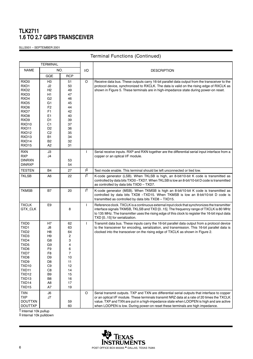
TLK27111.6 TO 2.7 GBPS TRANSCEIVERSLLS501 – SEPTEMBER 20016POST OFFICE BOX 655303 • DALLAS, TEXAS 75265Terminal Functions (Continued)TERMINALNAMENO.I/ODESCRIPTIONGQERCPI/ODESCRIPTIONRXD0RXD1RXD2RXD3RXD4RXD5RXD6RXD7RXD8RXD9RXD10RXD11RXD12RXD13RXD14RXD15H3J2H2H1G2G1F2F1E1D1C1D2C2B1B2A251504947464544424039373635343231OReceive data bus. These outputs carry 16-bit parallel data output from the transceiver to theprotocol device, synchronized to RXCLK. The data is valid on the rising edge of RXCLK asshown in Figure 5. These terminals are in high-impedance state during power-on reset.RXNRXPDINRXNDINRXPJ3J45354ISerial receive inputs. RXP and RXN together are the differential serial input interface from acopper or an optical I/F module.TESTENB427I‡Test mode enable. This terminal should be left unconnected or tied low.TKLSBA622I†K-code generator (LSB). When TKLSB is high, an 8-bit/10-bit K code is transmitted ascontrolled by data bits TXD0 –TXD7. When TKLSB is low an 8-bit/10-bit D code is transmittedas controlled by data bits TXD0 – TXD7.TKMSBB720I†K-code generator (MSB). When TKMSB is high an 8-bit/10-bit K code is transmitted ascontrolled by data bits TXD8 –TXD15. When TKMSB is low an 8-bit/10-bit D code istransmitted as controlled by data bits TXD8 – TXD15.TXCLKGTX_CLKE98IReference clock. TXCLK is a continuous external input clock that synchronizes the transmitterinterface signals TKMSB, TKLSB and TXD [0..15]. The frequency range of TXCLK is 80MHzto 135MHz. The transmitter uses the rising edge of this clock to register the 16-bit input dataTXD [0..15] for serialization.TXD0TXD1TXD2TXD3TXD4TXD5TXD6TXD7TXD8TXD9TXD10TXD11TXD12TXD13TXD14TXD15H7J8H8H9G8G9F9F8D9D8C9C8B9B8A8A7626364234671011121415161719ITransmit data bus. These inputs carry the 16-bit parallel data output from a protocol deviceto the transceiver for encoding, serialization, and transmission. This 16-bit parallel data isclocked into the transceiver on the rising edge of TXCLK as shown in Figure 2.TXNTXPDOUTTXNDOUTTXPJ6J75960OSerial transmit outputs. TXP and TXN are differential serial outputs that interface to copperor an optical I/F module. These terminals transmit NRZ data at a rate of 20 times the TXCLKvalue. TXP and TXN are put in a high-impedance state when LOOPEN is high and are activewhen LOOPEN is low. During power-on reset these terminals are high impedance.†Internal 10k pullup‡Internal 10k pulldown�
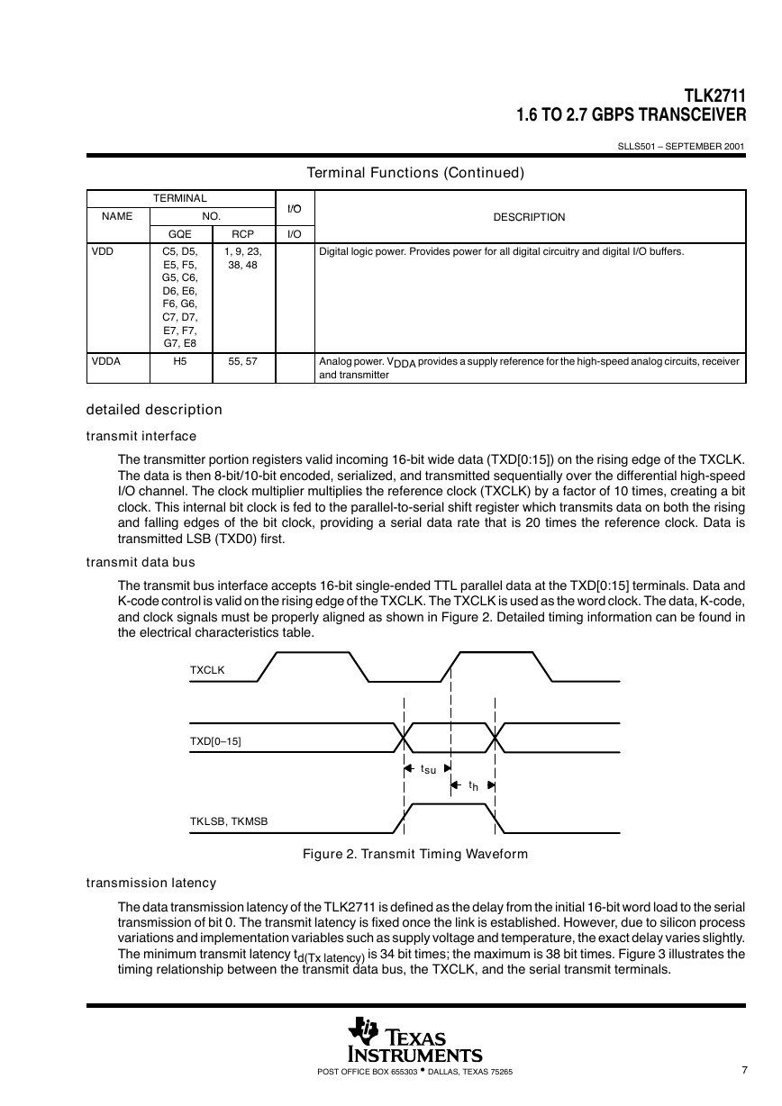
TLK27111.6 TO 2.7 GBPS TRANSCEIVERSLLS501 – SEPTEMBER 20017POST OFFICE BOX 655303 • DALLAS, TEXAS 75265Terminal Functions (Continued)TERMINALI/ONAMENO.I/ODESCRIPTIONGQERCPI/ODESCRIPTIONVDDC5, D5,E5, F5,G5, C6,D6, E6,F6, G6,C7, D7,E7, F7,G7, E81, 9, 23,38, 48Digital logic power. Provides power for all digital circuitry and digital I/O buffers.VDDAH555, 57Analog power. VDDA provides a supply reference for the high-speed analog circuits, receiverand transmitterdetailed descriptiontransmit interfaceThe transmitter portion registers valid incoming 16-bit wide data (TXD[0:15]) on the rising edge of the TXCLK.The data is then 8-bit/10-bit encoded, serialized, and transmitted sequentially over the differential high-speedI/O channel. The clock multiplier multiplies the reference clock (TXCLK) by a factor of 10 times, creating a bitclock. This internal bit clock is fed to the parallel-to-serial shift register which transmits data on both the risingand falling edges of the bit clock, providing a serial data rate that is 20 times the reference clock. Data istransmitted LSB (TXD0) first.transmit data busThe transmit bus interface accepts 16-bit single-ended TTL parallel data at the TXD[0:15] terminals. Data andK-code control is valid on the rising edge of the TXCLK. The TXCLK is used as the word clock. The data, K-code,and clock signals must be properly aligned as shown in Figure 2. Detailed timing information can be found inthe electrical characteristics table.TXCLKTXD[0–15]tsuthTKLSB, TKMSBFigure 2. Transmit Timing Waveformtransmission latencyThe data transmission latency of the TLK2711 is defined as the delay from the initial 16-bit word load to the serialtransmission of bit 0. The transmit latency is fixed once the link is established. However, due to silicon processvariations and implementation variables such as supply voltage and temperature, the exact delay varies slightly.The minimum transmit latency td(Tx latency) is 34 bit times; the maximum is 38 bit times. Figure 3 illustrates thetiming relationship between the transmit data bus, the TXCLK, and the serial transmit terminals.�
TLK27111.6 TO 2.7 GBPS TRANSCEIVERSLLS501 – SEPTEMBER 20018POST OFFICE BOX 655303 • DALLAS, TEXAS 75265detailed description (continued)16 bit Word to TransmitTransmitted 20 bit WordTXP,TXNTXD[0–15]TXCLKtd(Tx latency)Figure 3. Transmitter Latency8-bit/10-bit encoderAll true serial interfaces require a method of encoding to insure minimum transition density so that the receivingPLL has a minimal number of transitions to stay locked on. The encoding scheme maintains the signal dcbalance by keeping the number of ones and zeros the same. This provides good transition density for clockrecovery and improves error checking. The TLK2711 uses the 8-bit/10-bit encoding algorithm that is used byfibre channel and gigabit ethernet. This is transparent to the user, as the TLK2711 internally encodes anddecodes the data such that the user reads and writes actual 16-bit data.The 8-bit/10-bit encoder converts 8-bit wide data to a 10-bit wide encoded data character to improve itstransmission characteristics. Since the TLK2711 is a 16-bit wide interface, the data is split into two 8-bit widebytes for encoding. Each byte is fed into a separate encoder. The encoding is dependent upon two additionalinput signals, the TKMSB and TKLSB.Table 1. Transmit Data ControlsTKLSBTKMSB16 BIT PARALLEL INPUT00Valid data on TXD(0–7),Valid data TXD(8–15)01Valid data on TXD(0–7),K code on TXD(8–15)10K code on TXD(0–7),Valid data on TXD(8–15)11K code on TXD(0–7),K code on TXD(8–15)PRBS generatorThe TLK2711 has a built-in 27-1 PRBS (pseudorandom bit stream) function. When the PRBSEN terminal isforced high, the PRBS test is enabled. A PRBS is generated and fed into the 10-bit parallel-to-serial converterinput register. Data from the normal input source is ignored during the PRBS mode. The PRBS pattern is thenfed through the transmit circuitry as if it were normal data and sent out to the transmitter. The output can be sentto a BERT (bit error rate tester), the receiver of another TLK2711, or looped back to the receive input. Since thePRBS is not really random but a predetermined sequence of ones and zeroes, the data can be captured andchecked for errors by a BERT.parallel-to-serialThe parallel-to-serial shift register takes in the 20-bit wide data word multiplexed from the two parallel 8-bit/10-bitencoders and converts it to a serial stream. The shift register is clocked on both the rising and falling edge ofthe internally generated bit clock, which is 10 times the TXCLK input frequency. The LSB (TXD0) is transmittedfirst.�




 2023年江西萍乡中考道德与法治真题及答案.doc
 2012年重庆南川中考生物真题及答案.doc
 2013年江西师范大学地理学综合及文艺理论基础考研真题.doc
 2020年四川甘孜小升初语文真题及答案I卷.doc
 2020年注册岩土工程师专业基础考试真题及答案.doc
 2023-2024学年福建省厦门市九年级上学期数学月考试题及答案.doc
 2021-2022学年辽宁省沈阳市大东区九年级上学期语文期末试题及答案.doc
 2022-2023学年北京东城区初三第一学期物理期末试卷及答案.doc
 2018上半年江西教师资格初中地理学科知识与教学能力真题及答案.doc
 2012年河北国家公务员申论考试真题及答案-省级.doc
 2020-2021学年江苏省扬州市江都区邵樊片九年级上学期数学第一次质量检测试题及答案.doc
 2022下半年黑龙江教师资格证中学综合素质真题及答案.doc