applications
features
key specifications (typical)
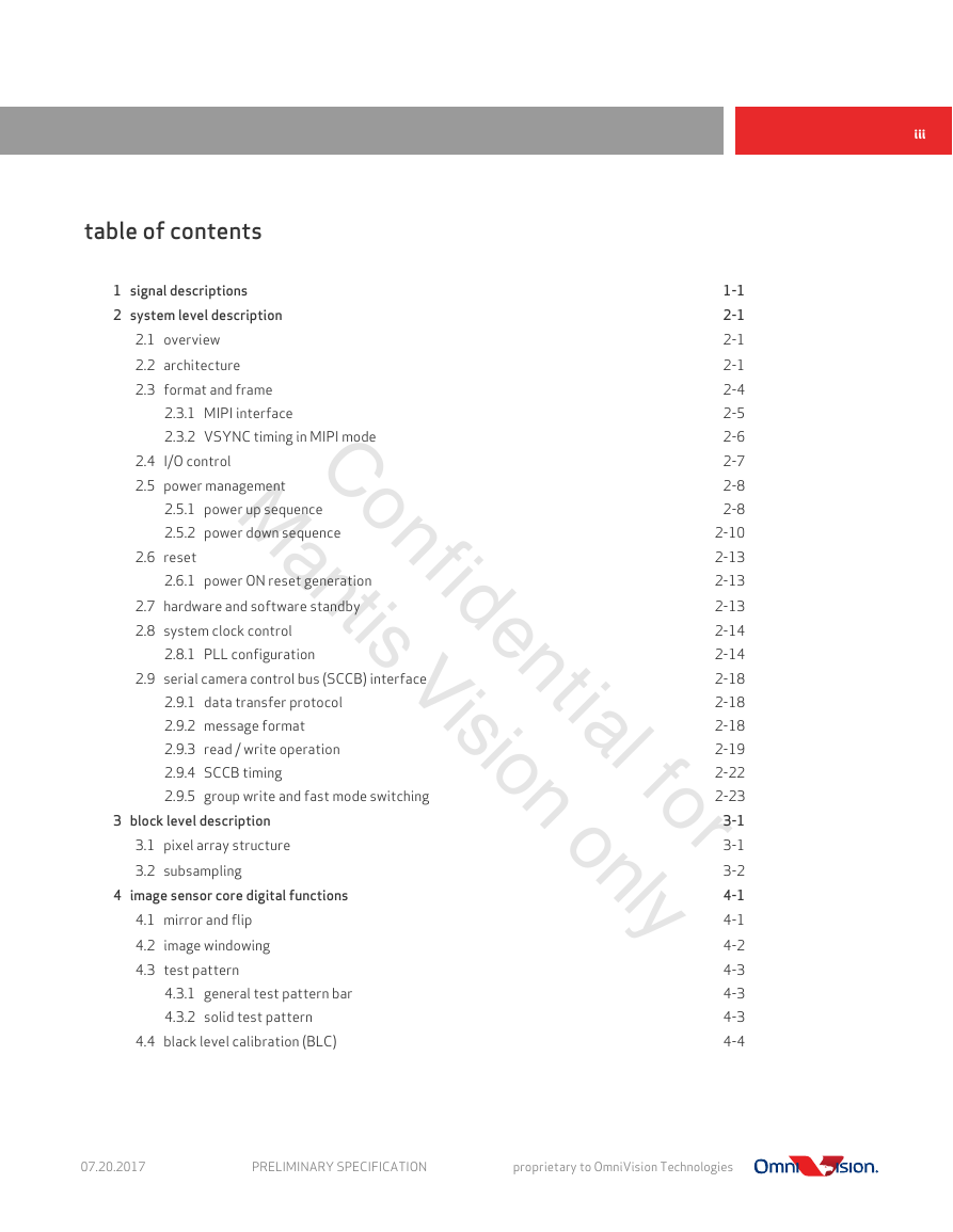
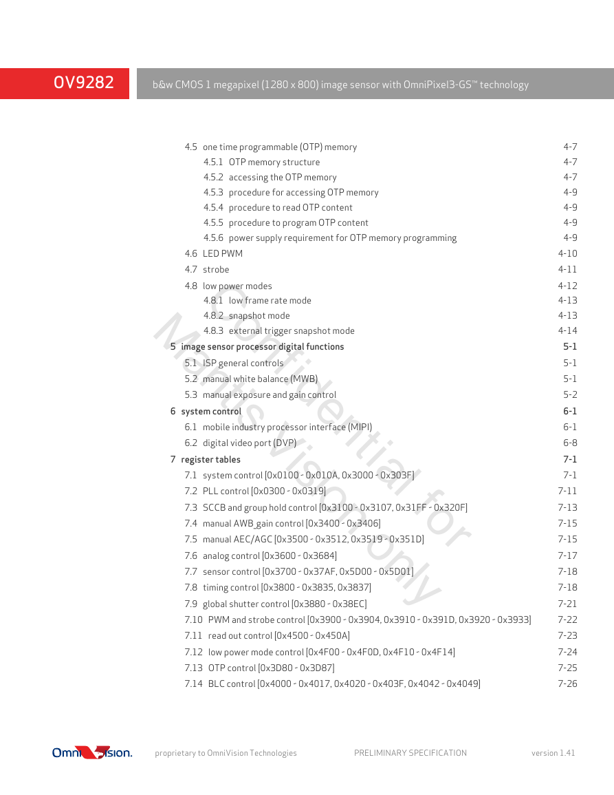
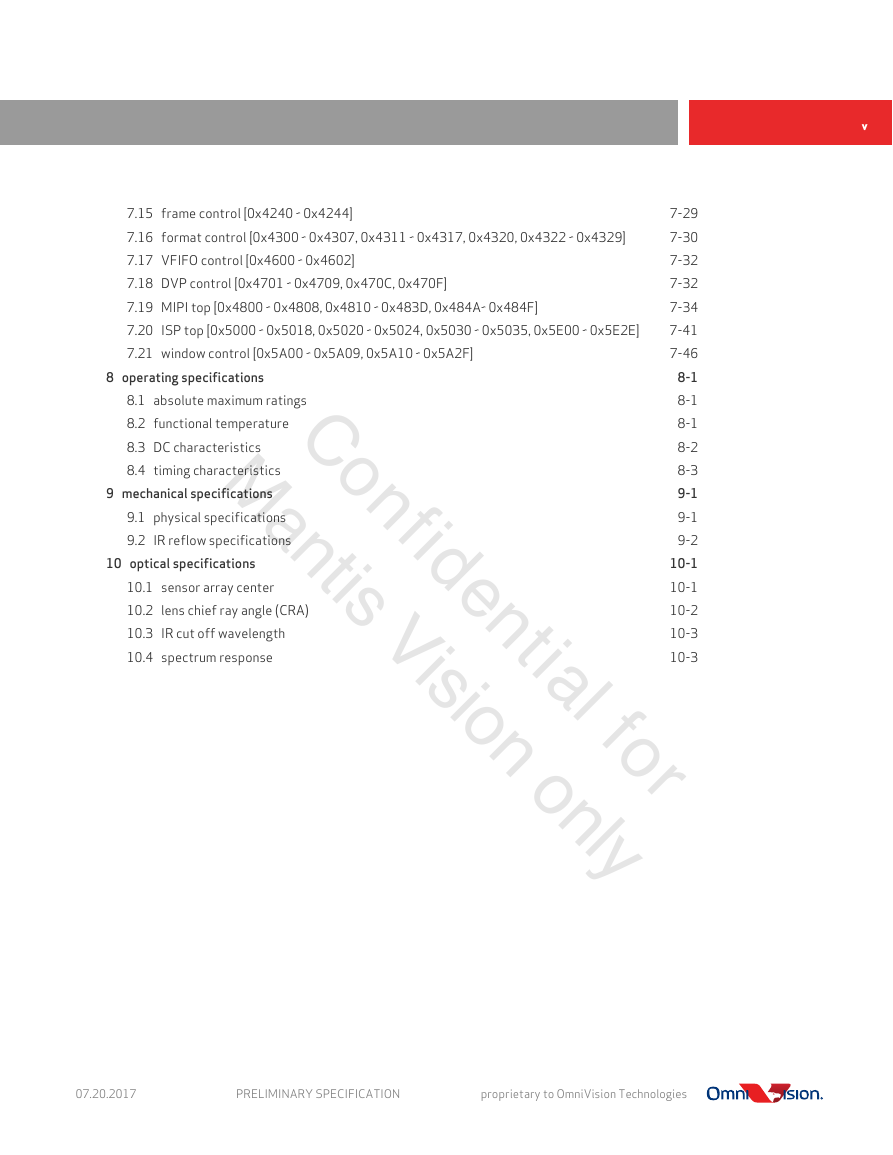
table of contents
list of figures
list of tables
1 signal descriptions
table 1-1 signal descriptions (sheet 1 of 3)
table 1-2 configuration under various conditions (sheet 1 of 2)
figure 1-1 pin diagram
table 1-3 pad symbol and equivalent circuit (sheet 1 of 2)
2 system level description
2.1 overview
2.2 architecture
figure 2-1 OV9282 block diagram
figure 2-2 OV9282 MIPI reference design schematic
figure 2-3 OV9282 DVP reference design schematic
2.3 format and frame
table 2-1 supported resolution and frame rate
2.3.1 MIPI interface
figure 2-4 MIPI timing
table 2-2 MIPI timing specifications (2-lane mode)
2.3.2 VSYNC timing in MIPI mode
figure 2-5 VSYNC timing in mode 1
figure 2-6 VSYNC timing in mode 2
figure 2-7 VSYNC timing in mode 3
2.4 I/O control
table 2-3 I/O control registers
2.5 power management
2.5.1 power up sequence
table 2-4 power up sequence
table 2-5 power up sequence timing constraints
figure 2-8 power up sequence
2.5.2 power down sequence
table 2-6 power down sequence
table 2-7 power down sequence timing constraints
figure 2-9 power down sequence
figure 2-10 standby sequence
2.6 reset
2.6.1 power ON reset generation
2.7 hardware and software standby
table 2-8 hardware and software standby description
2.8 system clock control
2.8.1 PLL configuration
figure 2-11 PLL1 clock diagram
figure 2-12 PLL2 clock diagram
table 2-9 PLL control registers (sheet 1 of 2)
table 2-10 sample PLL configuration
figure 2-13 clock connection diagram
table 2-11 PLL speed limitation
2.9 serial camera control bus (SCCB) interface
2.9.1 data transfer protocol
2.9.2 message format
figure 2-14 message type
2.9.3 read / write operation
figure 2-15 SCCB single read from random location
figure 2-16 SCCB single read from current location
figure 2-17 SCCB sequential read from random location
figure 2-18 SCCB sequential read from current location
figure 2-19 SCCB single write to random location
figure 2-20 SCCB sequential write to random location
2.9.4 SCCB timing
figure 2-21 SCCB interface timing
table 2-12 SCCB interface timing specifications
2.9.5 group write and fast mode switching
table 2-13 context switching control
3 block level description
3.1 pixel array structure
figure 3-1 sensor array layout
3.2 subsampling
figure 3-2 example of 2x2 binning
figure 3-3 example of 2:1 skipping
figure 3-4 example of 4:1 skipping
table 3-1 binning-related registers
4 image sensor core digital functions
4.1 mirror and flip
figure 4-1 mirror and flip samples
table 4-1 mirror and flip registers
4.2 image windowing
figure 4-2 image windowing
table 4-2 image windowing control functions
4.3 test pattern
4.3.1 general test pattern bar
figure 4-3 test pattern
table 4-3 general test pattern bar selection control
4.3.2 solid test pattern
table 4-4 solid color test pattern control (sheet 1 of 2)
4.4 black level calibration (BLC)
table 4-5 BLC control functions (sheet 1 of 2)
table 4-6 ALS algorithm control registers (sheet 1 of 3)
4.5 one time programmable (OTP) memory
4.5.1 OTP memory structure
table 4-7 OTP memory structure
4.5.2 accessing the OTP memory
figure 4-4 OTP access
4.5.3 procedure for accessing OTP memory
4.5.4 procedure to read OTP content
4.5.5 procedure to program OTP content
4.5.6 power supply requirement for OTP memory programming
4.6 LED PWM
figure 4-5 LED PWM output timing
table 4-8 LED PWM registers
table 4-9 non-volatile memory map table (OTP)
4.7 strobe
table 4-10 strobe control registers (sheet 1 of 2)
4.8 low power modes
table 4-11 low power mode control registers
4.8.1 low frame rate mode
figure 4-6 low frame rate mode timing
4.8.2 snapshot mode
figure 4-7 snapshot mode timing
4.8.3 external trigger snapshot mode
figure 4-8 external snapshot mode timing
figure 4-9 frame triggered by red pulse diagram
5 image sensor processor digital functions
5.1 ISP general controls
table 5-1 ISP top registers
5.2 manual white balance (MWB)
table 5-2 manual AWB_gain registers
5.3 manual exposure and gain control
table 5-3 manual exposure and gain control registers
6 system control
6.1 mobile industry processor interface (MIPI)
table 6-1 MIPI top control registers (sheet 1 of 7)
6.2 digital video port (DVP)
table 6-2 DVP control registers
7 register tables
7.1 system control [0x0100 ~ 0x010A, 0x3000 ~ 0x303F]
table 7-1 system control registers (sheet 1 of 10)
7.2 PLL control [0x0300 ~ 0x0319]
table 7-2 PLL control registers (sheet 1 of 3)
7.3 SCCB and group hold control [0x3100 ~ 0x3107, 0x31FF ~ 0x320F]
table 7-3 SCCB and group hold registers (sheet 1 of 3)
7.4 manual AWB_gain control [0x3400 ~ 0x3406]
table 7-4 manual AWB_gain registers
7.5 manual AEC/AGC [0x3500 ~ 0x3512, 0x3519 ~ 0x351D]
table 7-5 manual AEC/AGC registers (sheet 1 of 3)
7.6 analog control [0x3600 ~ 0x3684]
table 7-6 analog control registers
7.7 sensor control [0x3700 ~ 0x37AF, 0x5D00 ~ 0x5D01]
table 7-7 sensor control registers
7.8 timing control [0x3800 ~ 0x3835, 0x3837]
table 7-8 timing control registers (sheet 1 of 4)
7.9 global shutter control [0x3880 ~ 0x38EC]
table 7-9 DVP control registers
7.10 PWM and strobe control [0x3900 ~ 0x3904, 0x3910 ~ 0x391D, 0x3920 ~ 0x3933]
table 7-10 PWM and strobe control registers (sheet 1 of 2)
7.11 read out control [0x4500 ~ 0x450A]
table 7-11 read out control registers
7.12 low power mode control [0x4F00 ~ 0x4F0D, 0x4F10 ~ 0x4F14]
table 7-12 low power mode control registers (sheet 1 of 2)
7.13 OTP control [0x3D80 ~ 0x3D87]
table 7-13 OTP control registers
7.14 BLC control [0x4000 ~ 0x4017, 0x4020 ~ 0x403F, 0x4042 ~ 0x4049]
table 7-14 BLC control registers (sheet 1 of 4)
7.15 frame control [0x4240 ~ 0x4244]
table 7-15 frame control registers (sheet 1 of 2)
7.16 format control [0x4300 ~ 0x4307, 0x4311 ~ 0x4317, 0x4320, 0x4322 ~ 0x4329]
table 7-16 format control registers (sheet 1 of 2)
7.17 VFIFO control [0x4600 ~ 0x4602]
table 7-17 VFIFO control registers
7.18 DVP control [0x4701 ~ 0x4709, 0x470C, 0x470F]
table 7-18 DVP control registers (sheet 1 of 2)
7.19 MIPI top [0x4800 ~ 0x4808, 0x4810 ~ 0x483D, 0x484A~ 0x484F]
table 7-19 MIPI top control registers (sheet 1 of 8)
7.20 ISP top [0x5000 ~ 0x5018, 0x5020 ~ 0x5024, 0x5030 ~ 0x5035, 0x5E00 ~ 0x5E2E]
table 7-20 ISP top registers (sheet 1 of 6)
7.21 window control [0x5A00 ~ 0x5A09, 0x5A10 ~ 0x5A2F]
table 7-21 window control registers (sheet 1 of 5)
8 operating specifications
8.1 absolute maximum ratings
table 8-1 absolute maximum ratings
8.2 functional temperature
table 8-2 functional temperature
8.3 DC characteristics
table 8-3 DC characteristics (TA = 23°C ± 2°C)
8.4 timing characteristics
table 8-4 timing characteristics
9 mechanical specifications
9.1 physical specifications
figure 9-1 package specifications
table 9-1 package dimensions
9.2 IR reflow specifications
figure 9-2 IR reflow ramp rate requirements
table 9-2 reflow conditions
10 optical specifications
10.1 sensor array center
figure 10-1 sensor array center
10.2 lens chief ray angle (CRA)
figure 10-2 chief ray angle (CRA)
table 10-1 CRA versus image height plot
10.3 IR cut off wavelength
10.4 spectrum response
figure 10-3 spectrum response curve
revision history




 2023年江西萍乡中考道德与法治真题及答案.doc
 2012年重庆南川中考生物真题及答案.doc
 2013年江西师范大学地理学综合及文艺理论基础考研真题.doc
 2020年四川甘孜小升初语文真题及答案I卷.doc
 2020年注册岩土工程师专业基础考试真题及答案.doc
 2023-2024学年福建省厦门市九年级上学期数学月考试题及答案.doc
 2021-2022学年辽宁省沈阳市大东区九年级上学期语文期末试题及答案.doc
 2022-2023学年北京东城区初三第一学期物理期末试卷及答案.doc
 2018上半年江西教师资格初中地理学科知识与教学能力真题及答案.doc
 2012年河北国家公务员申论考试真题及答案-省级.doc
 2020-2021学年江苏省扬州市江都区邵樊片九年级上学期数学第一次质量检测试题及答案.doc
 2022下半年黑龙江教师资格证中学综合素质真题及答案.doc