InfoHub
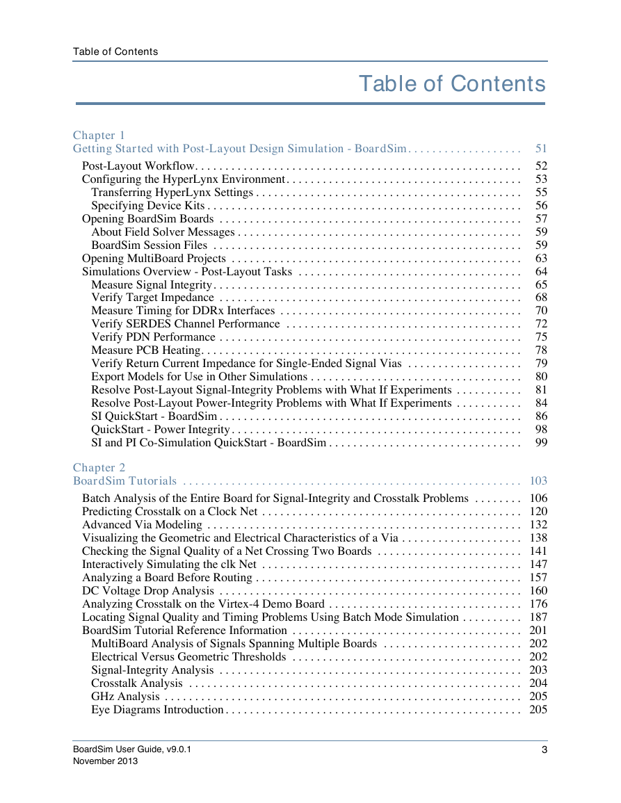
Table of Contents
List of Figures
List of Tables
Chapter 1 Getting Started with Post-Layout Design Simulation - BoardSim
Post-Layout Workflow
Configuring the HyperLynx Environment
Transferring HyperLynx Settings
Specifying Device Kits
Opening BoardSim Boards
About Field Solver Messages
BoardSim Session Files
Session File Types - BUD and BBD
Information Stored in Session Files
When to Not Save Session Files
Session Edits for Multiple Board Instances
When Session Files are Deleted
Missing Models and Packages
Opening MultiBoard Projects
Simulations Overview - Post-Layout Tasks
Measure Signal Integrity
Verify Target Impedance
Measure Timing for DDRx Interfaces
Verify SERDES Channel Performance
Verify PDN Performance
Measure PCB Heating
Verify Return Current Impedance for Single-Ended Signal Vias
Export Models for Use in Other Simulations
Resolve Post-Layout Signal-Integrity Problems with What If Experiments
Resolve Post-Layout Power-Integrity Problems with What If Experiments
SI QuickStart - BoardSim
Opening PCB Designs in BoardSim
Editing the Stackup
Mapping Reference Designators to Component Types
Editing Power-Supply Nets
Selecting Nets
Assigning IC Models
Editing Resistor - Inductor - Capacitor Values
Identifying Resistor and Capacitor Packages
Setting Up and Running Interactive Simulations
View Simulation Results
Measuring Timing and Voltage
Attaching Measurement Crosshairs to Waveforms
Recording Simulation Results
QuickStart - Power Integrity
SI and PI Co-Simulation QuickStart - BoardSim
Chapter 2 BoardSim Tutorials
Batch Analysis of the Entire Board for Signal- Integrity and Crosstalk Problems
Predicting Crosstalk on a Clock Net
Advanced Via Modeling
Visualizing the Geometric and Electrical Characteristics of a Via
Checking the Signal Quality of a Net Crossing Two Boards
Interactively Simulating the clk Net
Analyzing a Board Before Routing
DC Voltage Drop Analysis
Analyzing Crosstalk on the Virtex-4 Demo Board
Locating Signal Quality and Timing Problems Using Batch Mode Simulation
BoardSim Tutorial Reference Information
MultiBoard Analysis of Signals Spanning Multiple Boards
Electrical Versus Geometric Thresholds
Signal-Integrity Analysis
Crosstalk Analysis
GHz Analysis
Eye Diagrams Introduction
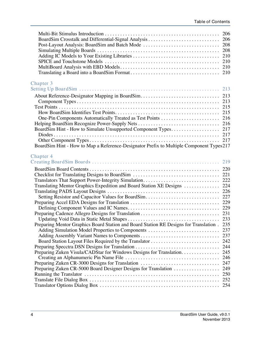
Multi-Bit Stimulus Introduction
BoardSim Crosstalk and Differential-Signal Analysis
How BoardSim Crosstalk Analysis Works
Using BoardSim Crosstalk for Differential-Signal Analysis
Automatically Finding Aggressor Nets
Post-Layout Analysis: BoardSim and Batch Mode
Simulating Multiple Boards
Other Analysis Features and MultiBoard Designs
Simulating with EBD Models
Adding IC Models to Your Existing Libraries
Adding IBIS Models
SPICE and Touchstone Models
MultiBoard Analysis with EBD Models
Translating a Board into a BoardSim Format
LineSim Tutorials
Chapter 3 Setting Up BoardSim
About Reference-Designator Mapping in BoardSim
Component Types
Reference-Designator Prefixes
Test Points
How BoardSim Identifies Test Points
One-Pin Components Automatically Treated as Test Points
Helping BoardSim Recognize Power-Supply Nets
BoardSim Hint - How to Simulate Unsupported Component Types
Diodes
Other Component Types
BoardSim Hint - How to Map a Reference- Designator Prefix to Multiple Component Types
Chapter 4 Creating BoardSim Boards
BoardSim Board Contents
Checklist for Translating Designs to BoardSim
Translators That Support Power-Integrity Simulation
Translating Mentor Graphics Expedition and Board Station XE Designs
Translating PADS Layout Designs
Setting Resistor and Capacitor Values for BoardSim
Preparing Accel EDA Designs for Translation
Defining Component Values and IC Names
Preparing Cadence Allegro Designs for Translation
Updating Void Data in Static Metal Shapes
Preparing Mentor Graphics Board Station and Board Station RE Designs for Translation
Adding Simulation Model Properties to Components
Adding Assembly Variant Names to Components
Variant Translation Examples
Configuring Layout to Create ASCII Files
Board Station Layout Files Required by the Translator
Preparing Specctra DSN Designs for Translation
Preparing Zuken Visula/CADStar for Windows Designs for Translation
Creating an Alphanumeric Pin Name File
Preparing Zuken CR-3000 Designs for Translation
Preparing Zuken CR-5000 Board Designer Designs for Translation
Running the Translator
Translate File Dialog Box
Translator Options Dialog Box
Chapter 5 Viewing BoardSim Boards
Board Viewer User Interface
Identifying Stackup Layers Used to Implement Trace Segments and Metal Shapes
Board Viewer Operations
Summary of Board Viewer Operations
Zooming and Panning
Viewing All Nets Simultaneously
Removing All Highlighting
Displaying Power-Supply Nets
Highlighting Decoupling and Bypass Capacitors
Highlighting Capacitor Mounting
Reviewing the Board Layout
Board Viewer Drawing Details
Board Outline
Component Outlines
Pads
Anti-Pads
Drill Holes
Pins
Pin Numbers
Pin Names
Unattached Reference Designators
Chapter 6 Setting Up Boards for Signal-Integrity Simulation
Selecting Nets for SI Analysis
Associated Nets
Selecting Nets by Name
Sorting Nets
Net Lengths
Net Lengths Reported are Pre-Cleanup Unless Enable Net Cleaning During Loading Option is Enabled
Viewing Net Lengths Including Associated Nets and Cleanup
Viewing Clean-Up Net Lengths
Selecting Nets by Reference Designator
Net Lengths
Selecting Nets by Location in the Board Viewer
Editing Power-Supply Net Properties
Why Power-Supply Nets Matter
How BoardSim Identifies Power-Supply Nets
Identifying by Name Matching
Automatic Net Names
VCC
GND
Inferred Net Names
Identifying by Counting Capacitors
Identifying by Counting Metal Segments
Undetected Power-Supply Nets
Editing Power-Supply Nets
Sorting Power-Supply Nets
Removing Non-Functional Pads from Signal Vias
Editing Trace Widths in BoardSim
Changing Trace Widths
How to Change Trace Widths
Choosing Which Segments to Change
Choosing Which Nets
Choosing Which Layers
Choosing a Range of Widths
Conditions are ANDed
Restoring Original Widths
Possible Bad Effects from Width Changes
Width Changes Not Reported in Design Change Summary
Examples of Changing Trace Widths
Changing an Entire Single Trace on All Its layers
Changing All Traces on a Single Stackup Layer
Changing All 10-Mil and 8-Mil Traces to 6 Mils Wide
Changing the Top-Layer 6-Mil Segments on Net CLK to 8 Mils Wide
Reasons Why You Must Select Models
Comparing Model-Selection Methods
About Interactive and Automapping Model Assignment Methods
Characteristics Not Shared by IC-Model Selection Methods
EBD and IBIS Series Bus Switch Models Cannot be Assigned Interactively
Interactive Method Enables Experimentation
An Example to Contrast Interactive and Automapping Methods
Tradeoffs Between REF and QPL Automapping Files
Precedence Among Model and Value Selection Methods
Troubleshooting Unexpected Model Selection Results
Precedence Error
REF or QPL File Syntax Error
Invalid REF or QPL Model Mapping
QPL Automapping has Been Disabled
QPL File or Directory Name Error
Selecting Models and Values for Individual Pins
Selecting Models and Values for Entire Components
About REF and QPL Automapping Files
How Automapping Works
ICs
Resistors and Capacitors
Default Buffer Direction of Pins Selected by Automapping Files
Using Multiple IC Model-Assignment Methods
Creating Automapping Files
Locations and Names of Automapping Files
Editing REF Files
About the REF-File Editor User Interface
Selecting REF File Spreadsheet Rows
Filtering REF File Reference Designator Spreadsheets
Editing a .REF File
Editing Composite REF Files for MultiBoard Projects
About Part Names in BoardSim
QPL File Editor
Selecting QPL File Spreadsheet Rows
Finding Text in the Assignment Spreadsheet
Format of REF and QPL Files
Example REF File
Example QPL File
Formatting Shared by REF and QPL Files
Units for Resistor, Capacitor, and Inductor Values
Formatting Unique to .REF Files
Formatting Unique to .QPL Files
Debugging Errors in REF and QPL Files
Syntax Errors in REF Files
Syntax Errors in QPL Files
Model Contents and Model Location Errors
Errors Reported During Interactive Signal-Integrity Simulation
Errors Reported During Batch Signal-Integrity Simulation
Example REF File Errors
Example QPL File Errors
Temporarily Disabling REF and QPL Files
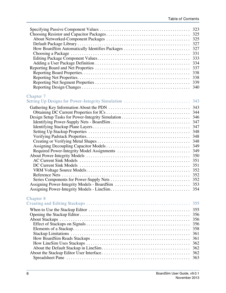
Specifying Passive Component Values
Choosing Resistor and Capacitor Packages
About Networked-Component Packages
Supported Component Types
Supported Connection Styles
How Networked-Component Packages Affect Signal-Integrity Simulation
Default Package Library
Elements of a Package Definition
How BoardSim Automatically Identifies Packages
Details of Package Matching
Determining There is a Package
Package Shape
Number of Pins
By Counting Connections
By Looking at Pin Names
Limitations on Automatic Pin Counting
Connection Style
Final Matching
If Matching Problems Occur
If No Match is Found
If Multiple Matches are Found
Next-Bigger Packages Included - In the Select Package Dialog Box
Next-Bigger Packages Included - During Automatic Selection
Choosing a Package
Selecting a Package For a Networked Resistor or Capacitor
The Packages List
The Connectivity Picture
Editing Package Component Values
Editing Component Values for Series-Style Packages
Editing Component Values for Pullup-Style Packages
Editing Component Values for Pullup- and Pulldown-Style Packages
Adding a User Package Definition
Reasons for Creating a Custom Package
How User Package Library Supplements Default Package Library
Syntax for Package Definitions
How to Create a Custom Package Definition
User Package Library Example - Defining a New Package
Saving User Package Libraries
Reporting Board and Net Properties
Reporting Board Properties
Reporting Net Properties
Report Description
Reporting Net Segment Properties
Viewing Net Segment Properties
Viewing Net Segment Field-Solver Output
Viewing Net Segment Attenuation Over a Frequency Range
Reporting Design Changes
Chapter 7 Setting Up Designs for Power-Integrity Simulation
Gathering Key Information About the PDN
Obtaining DC Current Properties for ICs
Design Setup Tasks for Power-Integrity Simulation
Identifying Power-Supply Nets - BoardSim
Identifying Stackup Plane Layers
Setting Up Stackup Properties
Verifying Padstack Properties
Creating or Verifying Metal Shapes
Assigning Decoupling Capacitor Models
Required Power-Integrity Model Assignments
About Power-Integrity Models
AC Current Sink Models
DC Current Sink Models
VRM Voltage Source Models
Reference Nets
Series Components for Power-Supply Nets
Assigning Power-Integrity Models - BoardSim
Assigning Power-Integrity Models - LineSim
Chapter 8 Creating and Editing Stackups
When to Use the Stackup Editor
Opening the Stackup Editor
About Stackups
Effect of Stackups on Signals
Stackup Parameters That Affect Impedance and Velocity
Elements of a Stackup
Plane Layers
Assumption About Plane Layers
Plane Layers in LineSim
Plane Layers in BoardSim
Signal Layers
Microstrip
Buried Microstrip
Stripline
Dielectric Layers
Dielectric Constants
Plating Layers
Stackup Limitations
How BoardSim Reads Stackups
How LineSim Uses Stackups
About the Default Stackup in LineSim
About the Stackup Editor User Interface
Spreadsheet Pane
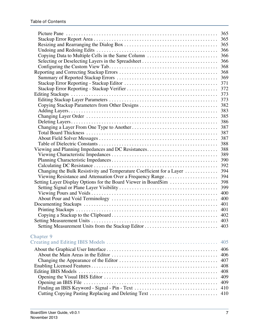
Picture Pane
Stackup Error Report Area
Resizing and Rearranging the Dialog Box
Undoing and Redoing Edits
Copying Data to Multiple Cells in the Same Column
Selecting or Deselecting Layers in the Spreadsheet
Common Layer Selection and Deselection Tasks
Configuring the Custom View Tab
Reporting and Correcting Stackup Errors
Summary of Reported Stackup Errors
No Stackup at All
Missing Layers
Missing Signal Layers
Missing Plane Layers
Missing Dielectric Layers
Zero Thicknesses
Zero Dielectric Constants
Negative Dielectric Loss Tangent
Negative Metal Layer Resistivity
Metal Usage Threshold Exceeded for Signal Layer
Stackup Error Reporting - Stackup Editor
Stackup Error Reporting - Stackup Verifier
Editing Stackups
Editing Stackup Layer Parameters
Dielectric Layer Parameters
Thickness and Dielectric Constant
Dielectric Layer Name
Usage Parameter for Dielectric Layers
Technology
Loss Tangent
Thermal Conductivity - Dielectric
Plane or Signal Layer Parameters
Thickness
Layer Name
Layer Names in LineSim
Layer Names in BoardSim
Usage Parameter for Metal Layers
Metal
Bulk Resistivity
Temperature Coefficient
Dielectric Constant
Loss Tangent
Thermal Conductivity
Calculated Dielectric Permittivity and Loss Tangent for Metal Layers
Copying Stackup Parameters from Other Designs
Adding Layers
Setting Default Layer Parameters
Adding Dielectric Layers
Adding Plane Layers
Adding Signal Layers
Adding the Most-Suitable Layer
Changing Layer Order
Deleting Layers
Cannot Delete Signal Layers with Routing
Deleting Signal Layers in BoardSim
Deleting Signal Layers in LineSim
Changing a Layer From One Type to Another
Planes With Signal Routing
Changing a Layer Type
Total Board Thickness
About Field Solver Messages
Table of Dielectric Constants
Viewing and Planning Impedances and DC Resistances
Viewing Characteristic Impedances
Calculating the Characteristic Impedance for Schematics
Calculating the Characteristic Impedance for Boards
Calculating the Characteristic Impedance For a Test Trace Width
About Test Trace Widths in BoardSim
Planning Characteristic Impedances
Single Traces
Differential Pairs
Calculating Trace Separation For a Differential Pair
Calculating Trace Width For a Differential Pair
Calculating Trace Separation and Width For a Differential Pair
Calculating DC Resistance
Bulk Resistivity and Temperature Coefficient
How Resistivity - Temperature Coefficient - Temperature Are Used
Simulation Temperature
Changing the Bulk Resistivity and Temperature Coefficient for a Layer
Viewing Resistance and Attenuation Over a Frequency Range
Displaying Loss Versus Frequency in the Edit Transmission Line Dialog Box
Displaying Loss Versus Frequency in the Stackup Editor
Displaying Loss Versus Frequency in BoardSim
Examining and Documenting Curves
Setting Layer Display Options for the Board Viewer in BoardSim
Changing Stackup Layer Colors
Setting Signal or Plane Layer Visibility
Viewing Pours and Voids
About Pour and Void Terminology
Documenting Stackups
Printing Stackups
Printing the Stackup Spreadsheet
Printing the Stackup Picture
Setting Up For Printing
Copying a Stackup to the Clipboard
Copying Stackup Manufacturing Documentation to the Clipboard
Copying Stackup Pictures to the Clipboard
Setting Measurement Units
Setting Measurement Units from the Stackup Editor
Chapter 9 Creating and Editing IBIS Models
About the Graphical User Interface
About the Main Areas in the Editor
Changing the Appearance of the Editor
Resizing the Editor Dialog Box or Internal Panes
Hiding or Displaying Editor Windows or Menus
Setting Font Color and Tab Preferences
Enabling Licensed Features
Editing IBIS Models
Opening the Visual IBIS Editor
Opening an IBIS File
Finding an IBIS Keyword - Signal - Pin - Text
Cutting Copying Pasting Replacing and Deleting Text
Cutting Text
Copying Text
Pasting Text
Replacing Text
Deleting Text
Undoing or Redoing an Edit
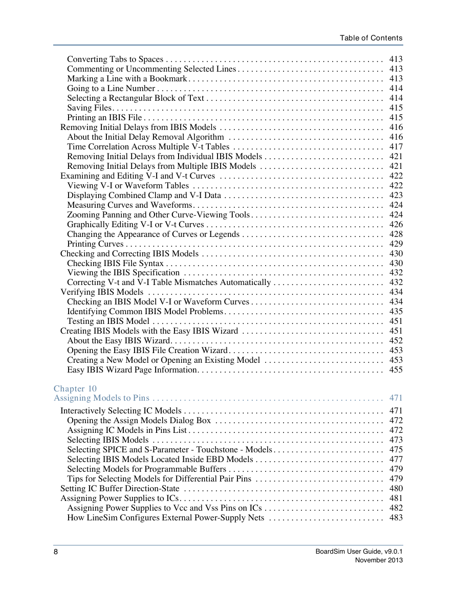
Converting Tabs to Spaces
Commenting or Uncommenting Selected Lines
Marking a Line with a Bookmark
Going to a Line Number
Selecting a Rectangular Block of Text
Saving Files
Printing an IBIS File
Removing Initial Delays from IBIS Models
About the Initial Delay Removal Algorithm
Time Correlation Across Multiple V-t Tables
All Tables Correlated
Rising and Falling Tables Treated Separately
Corners Treated Separately
Removing Initial Delays from Individual IBIS Models
Removing Initial Delays from Multiple IBIS Models
Examining and Editing V-I and V-t Curves
Viewing V-I or Waveform Tables
Displaying Combined Clamp and V-I Data
Measuring Curves and Waveforms
Zooming Panning and Other Curve-Viewing Tools
Resizing the View IBIS Data Dialog Box
Zooming to Selection
Fitting the Curve to Window
Fitting the Curve to User-Defined Extents
Tracking Curves and Waveforms
Panning in the IBIS Editor
Graphically Editing V-I or V-t Curves
Changing the Appearance of Curves or Legends
Plotting Table Data Using Curves Points or Both
Changing Data Point Size
Changing Curve and View Colors
Changing Legend Font
Printing Curves
Checking and Correcting IBIS Models
Checking IBIS File Syntax
Running the Syntax Checker on IBIS Models
Jumping to a Line in the IBIS Model Containing a Syntax Violation
Resolving Errors and Warnings
Viewing the IBIS Specification
Correcting V-t and V-I Table Mismatches Automatically
Verifying IBIS Models
Checking an IBIS Model V-I or Waveform Curves
Identifying Common IBIS Model Problems
Data Have the Wrong Sign
Syntax Example for Data Have the Wrong Sign
Graphical Example for Data Have the Wrong Sign
Special Explanation for Pullup Data
Data Have the Wrong Units
Graphical Example for Data Have the Wrong Units
Data Have Noise Properties
Graphical Example for Data Have Noise Properties
Data Have Non-Monotonic Properties
Syntax Example for Data Have Non-Monotonic Properties
Graphical Example for Data Have Non-Monotonic Properties
Data Have Spurious Points
Syntax Example for Data Have Spurious Points
Graphical Example for Data Have Spurious Points
Data Do Not Follow Typ-Min-Max Order
Syntax Example for Data Do Not Follow Typ-Min-Max Order
Graphical Example for Data Do Not Follow Typ-Min-Max Order
V-I Table Data Do Not Pass Through the Origin
Graphical Example for V-I Table Data Do Not Pass Through the Origin
V-t or V-I Table Data are Missing
V-t and V-I Table Data are Mismatched
Load Line Analysis Example
Syntax Example for V-t and V-I Table Data are Mismatched
Paired Curves Do Not Have the Opposite Polarity
Ramp Table Data Have Zero or Negative Values
Vmeas Voltage Does Not Cross V-I Data
Syntax Example for Vmeas Voltage Does Not Cross V-I Data
Testing an IBIS Model
Creating IBIS Models with the Easy IBIS Wizard
About the Easy IBIS Wizard
Text String Restrictions
Data Requirements
Limitations for the Wizard
About Hints Displayed by the Wizard
Opening the Easy IBIS File Creation Wizard
Creating a New Model or Opening an Existing Model
Creating New IBIS Models
Opening Existing IBIS Models
Resetting the Wizard
Easy IBIS Wizard Page Information
Setting Model Name Type and Technology
Entering Header Information
Choosing a Pre-Defined Buffer Model
About the Pre-Defined Buffer Models that Ship with the Wizard
Mapping Power and Ground Pins
Single-Pin versus Multi-Pin Models
Specifying Clamp Diodes
Setting Operating Voltage - Die Capacitance - Thresholds - Scaling Factors
Specifying Pull-Up and Pull-Down Buffers
Specifying Pull-Up Buffers
Specifying Pull-Down Buffers
Specifying Output Polarity and Load Circuit
Entering Pin Data - Selecting Buffers - Creating or Editing the Model
About the Pin Table
Modifying Pin Data and Selecting Buffers
Creating the IBIS Model
What to do With the New Model You Have Just Created
Creating - Editing - Deleting Buffer Models
How the Wizard Models Buffers
Pre-Defined Versus User-Created Buffer Models
Creating a New Buffer Model
Editing an Existing Buffer Model
Deleting an Existing Buffer Model
Entering Notes
Entering Package Pin Count and Parasitics
Predefined versus User-Defined Packages
Entering Min-Max Scaling
Entering Data Source and Disclaimer Information
Determining Output Impedance
Measuring from Published V-I Curves
Extracting Driver Resistance from a SPICE Model
Procedure
Chapter 10 Assigning Models to Pins
Interactively Selecting IC Models
Opening the Assign Models Dialog Box
Assigning IC Models in Pins List
Selecting IBIS Models
Selecting SPICE and S-Parameter - Touchstone - Models
Selecting IBIS Models Located Inside EBD Models
Selecting Models for Programmable Buffers
Tips for Selecting Models for Differential Pair Pins
With IBIS Differential Model - Pin Names Must Match PCB - BoardSim
How to Tell if an IBIS Model is Differential
Setting IC Buffer Direction-State
Assigning Power Supplies to ICs
Assigning Power Supplies to Vcc and Vss Pins on ICs
How LineSim Configures External Power-Supply Nets
How BoardSim Configures External Power-Supply Nets
Importance of Power-Supply Pin Location in BoardSim EMC
Copying Models
Copying an Existing Model
Pasting to Another IC Pin
Pasting to All Other IC Pins
Creating Multiple Receivers and One Driver of the Same Type
Removing Models
Removing Interactively-Assigned Models
Cannot Interactively Remove Automapping Assignments
Session-File Example
Interactive Model Example
Reference Information for Selecting Models Interactively
About the Assign Models Dialog Box
Pins List
IC Reference Designators in BoardSim
IC Reference Designators in LineSim
Pins List Icons
Models Area
Component-Type Icons
Component-Data Information
Additional Icons for Networked Resistors and Capacitors
Component-Type Tabs
Buffer Area
Possible Buffer States
Input Versus Output Hi-Z
Threshold Voltages
Viewing Series Bus Switch Pin Connectivity
Enabling Series Bus Switches for Simulation
Design File List in BoardSim
Design File List in LineSim
Apply to All Similar Boards Check Box
Reference Designator and Pin Name Boxes
Using the Port-Mapping Spreadsheet
Connecting Model Ports to the Circuit
Connection Types
SPICE Output Characteristics
Port-Mapping Example - Connecting Non-Differential SPICE Models
Port-Mapping Example - Connecting Differential SPICE Models
About the Select IC Model Dialog Box
Information on Selected Device Area
Select a Library Device and Signal-Pin Area
Filtering the Contents of the Libraries List
Finding a Model in a Library
Shipping Model Library
Select By Area
Default IC Model Direction and State
If Second Pin is Not Visible
Searching for Models
About IC Models
How ICs are Modeled for Signal-Integrity Simulation
IC-Model Formats
IC Model Comparison
Obtaining IC Models from Semiconductor Vendors
The IBIS Format
IBIS - I-O Buffer Information Specification
The EBD - Electrical Board Description - Format
Supply and Non-Supply Mismatches for EBD Models and HYP File
Editing IBIS IC Models
How to Create a Custom IC Model
Creating an IBIS Model
Chapter 11 Interactively Simulating Signal Integrity
Oscilloscope and EZwave Comparison
Interactive SI Simulation Workflow - Oscilloscope
Editing the Waveform Wrapping Start Time for Eye Diagrams in the Oscilloscope
Miscellaneous SPICE Simulation Information
SPICE Netlist and Run Files
Interactive SI Simulation Workflow - EZwave
Displaying Waveforms Stored in the EZwave Database
SI Simulation Options
Enable Crosstalk Simulation in BoardSim
Enable Crosstalk Simulation in LineSim
Enabling Lossy Transmission-Line Modeling
Enabling Surface Roughness Modeling
Enabling Via Modeling
Removing Non-Functional Pads from Simulation
Define Driver Stimulus
Global and Per-Net/Pin Stimulus Overview
Assigning Per-Net/Pin Stimulus
Editing Per-Net/Pin Stimulus
Create Custom Bit Patterns
Creating Bit Patterns with a Text Editor
Creating Bit Patterns Numerically with the Bit-Pattern Editor
Creating Bit Patterns Graphically with the Bit-Pattern Editor
Measure Waveforms and Eye Diagrams
Automatically Measure Waveforms and Eye Diagrams
Automatic Measurements Overview and Descriptions
High and Low Level Voltages - V_high and V_low
Measurement Threshold Voltages - V_high_ref and V_low_ref
Rising and Falling Overshoot
Peak-to-Peak Voltage
Rise and Fall Time
Rise and Fall Slew Rate
Compensated Flight Time
Eye Width
Eye Height
Automatic Measurements Availability
Correlation Between Oscilloscope and Batch Simulation Measurements
Displaying Three Consecutive Simulations
Editing Eye Mask Properties
Edit Lossy Properties
Editing Lossy Properties in the Stackup Editor
Editing Lossy Properties in the Edit Transmission Line Dialog Box
Oscilloscope Probes
Manually Attaching Differential Probes
Swapping Differential Probe Polarity
Probe SPICE Ports Not Connected to the Net
Probe Where There is No Component - Signal Integrity
Eye Diagram Analysis Overview
Reasons to Run Eye Diagram Analysis
Standard Eye Diagram Overview
Co-Simulation Overview
Sweeps Overview
IBIS Model Sweeping Uses Internal Supply Values
BoardSim Sweeps Do Not Support Electrical Coupling Thresholds
Unrouted Trace Segment Sweeps in BoardSim
Manage the Number of Sweep Simulations
Disable Specific Sweep Values Within a Range
Disable Specific Sweep Simulations
Chapter 12 Simulating Signal Integrity with IBIS-AMI Channel Analysis
IBIS-AMI Channel Analysis QuickStart
IBIS-AMI Channel Analysis Overview
Statistical and Time Domain Simulation Comparison
IBIS-AMI Model Quality Factors for Statistical Simulation
IBIS-AMI Sweep Simulation Calculations
Chapter 13 Simulating Signal Integrity with FastEye Channel Analysis
FastEye Channel Analysis QuickStart
FastEye Channel Analysis Overview
FastEye Channel Analysis Simulation Flow
Checking Channels for Linear and Time-Invariant Behavior
Worst-Case Bit Patterns Overview
Model Channel Frequency Response with Complex-Pole Models
Bit Sequence for Automatic Channel Characterization
FastEye Diagram Measurements
Measuring FastEye Diagrams
Measuring FastEye Diagrams Automatically
About Automatic FastEye Diagram Measurements
Measuring FastEye Diagrams Manually
Using Measurement Crosshairs
Performing Measurements with the Mouse Pointer
Adding an Eye Mask to FastEye Diagrams
Zooming and Examining FastEye Diagrams
Chapter 14 Simulating DDRx Memory Interfaces
Preparing Designs for DDRx Batch Simulation
DDRx Batch Simulation Requirements
Gathering Information About Your DDRx Memory Interface and Design
DDRx Topologies
Topology for JEDEC Standard UDIMM - DDR, DDR2, DDR3
Topology for JEDEC Standard RDIMM - DDR and DDR2
Topology for JEDEC Standard RDIMM - DDR3
Topology for Non-JEDEC Standard DDRx - Register Only or PLL Only
Setting Up HyperLynx for DDRx Simulation - Design Files and Models
Creating Controller and DRAM Timing Models
Required Controller Timing Parameters
Review of DDRx Timing Relationships
Adding Model Selector Keywords to IBIS Models
Verifying the Design Setup for DDRx Batch Simulation
DDRx Background Information
Data Flow for DDRx Batch Simulation
Mapping DDRx Interface Signals to Nets in the Design
Pairing DDRx Interface Signals
Supported IBIS Model Spec and Receiver Threshold Keywords
On-Die Termination - ODT
Derating DDR2 and DDR3 Setup and Hold Times
Step 1 - Measuring Raw Setup and Hold Timing
Setup and Hold Measurements - Differential Clock or Strobe
Setup and Hold Measurements - Single-Ended Clock or Strobe
Step 2 - Obtaining Slew Rates for Derating Tables
Plotting Nominal Slew-Rate Lines for Setup Measurements
Plotting Nominal Slew-Rate Lines for Hold Measurements
Plotting Tangental Slew-Rate Lines for Setup Measurements
Plotting Tangental Slew-Rate Lines for Hold Measurements
Step 3 - Calculating Derated Setup and Hold Times
Physical Basis of DDR2 and DDR3 Slew-Rate Derating
Effects of Delay Ranges on Setup and Hold Measurements
Write Leveling for DDR3
DDR3 Write Leveling Delay File
DDR3Delays_autogenerated.txt File Format
DDR3 Delay File Measurements
Schematic Setup for DDRx Batch Simulation
Reference Designators
Net Names
Comments
Round Robin for DDRx Batch Simulation
About Measuring DDRx Signals with Eye Diagrams
Running DDRx Batch Simulation
Running DDRx Simulation for the First Time
Procedure to Run DDRx Batch Simulation
Creating DDR3 Write Leveling Delay Files
DDRx Batch Simulation Results
DDRx Results Spreadsheets
Stimulus Offset and Initial Delay Delta
DDRx Data Spreadsheets
DDRx Address Spreadsheets
DDRx Skew Spreadsheets
DDRx JEDEC Measurements Spreadsheets
DDRx Clock Jitter Spreadsheets
DDRx Clock Jitter Error Spreadsheets
DDRx Round Trip Time Spreadsheets
DDRx Wizard Pages Affecting Spreadsheet Contents
DDRx Waveform Files
DDRx Waveforms - Sub-folders
DDRx Waveforms - Files
DDRx Log File
DDRx Audit Spreadsheet
Switch to CSV Format for Very Large _allcases_ Files
DDRx Batch-Mode Wizard Dialog Boxes
DDRx Batch-Mode Wizard - Introduction Page
Selecting Spreadsheet Rows in the DDRx Wizard
DDRx Batch-Mode Wizard - Initialization Page
DDRx Batch-Mode Wizard - Controller Page
DDRx Batch-Mode Wizard - DRAMs Page
Specifying Locations for Stacked-Die DRAMs
DDRx Batch-Mode Wizard - PLLs and Registers Page
DDRx Batch-Mode Wizard - IBIS Models Page
DDRx Batch-Mode Wizard - Nets to Simulate Page
DDRx Batch-Mode Wizard - DRAM Signals Page
DDRx Batch-Mode Wizard - Data Strobes Page
DDRx Batch-Mode Wizard - Data Nets Page
DDRx Batch-Mode Wizard - Clock Nets Page
DDRx Batch-Mode Wizard - Address and Command Nets Page
DDRx Batch-Mode Wizard - Control Nets Page
DDRx Batch-Mode Wizard - Disable Nets Page
DDRx Batch-Mode Wizard - ODT Models Page
DDRx Batch-Mode Wizard - ODT Behavior Page
DDRx Batch-Mode Wizard - IBIS Models Selectors Page
DDRx Batch-Mode Wizard - Timing Models Page
DDRx Batch-Mode Wizard - Round Trip Time Page
RTT_Limits.txt File Format
Map Custom Data Rates to Standard JEDEC Derating Tables
DDR2 - Mapping Custom Data Rates to Standard Derating Tables
DDR3 - Mapping Custom Data Rates to Standard Derating Tables
DDRx Batch-Mode Wizard - Write Leveling Page
DDRx Batch-Mode Wizard - Sweep Manager Page
DDRx Batch-Mode Wizard - Stimulus and Crosstalk Page
DDRx Batch-Mode Wizard - Simulation Options Page
DDRx Batch-Mode Wizard - Quality Checks Page
DDRx Batch-Mode Wizard - Report Options Page
DDRx Batch-Mode Wizard - Simulate Page
DDRx Batch-Mode - Run Simulation Dialog Box
Chapter 15 Batch Simulating Signal Integrity
Generic and Advanced Batch Simulation Comparison
Batch SI Simulation Feature Comparison
Batch SI Simulation Crosstalk Thresholds
Batch SI Simulation Workflow - Generic
Batch SI Simulation Workflow - Advanced
Reference Information - Generic Batch Simulation Only
Compare Quick Analysis and Detailed Simulation
Generic Batch SI Simulation Reports
Summary Report Contents
CSV and XLS Report Contents
Differential Measurements in Batch SI Simulation
Driver IC Behavior During Generic Batch Crosstalk Simulation
Driver Logic State Switching
Importance of the Victim Net Stuck State
Buffer Inversion Affects the Stuck State
Aggressor Net Drivers Switch Together
Results of Missing or Incorrectly-Enabled IC Models
High-Accuracy Mode for Batch Simulation
Effects of High-Accuracy Mode on Differential Signals
Reference Information - General
Net Mapping Between CES and BoardSim
Constraint Mapping Between CES and BoardSim
Chapter 16 Simulating Multiple-Board Designs
Getting Started with MultiBoard
MultiBoard Project Limitations
Unavailable Features
Maximum Number of Boards
Modeling Board-to-Board Interconnections
Types of Board-to-Board Interconnection Models
About Simple Interconnection Models
Mated and Unmated Electrical Characteristic Values
Special Case - Edge Connector
Nets are Associated by Interconnect Models
MultiBoard Project Wizard Overview
About Board IDs
Mapping a HYP File to a Board ID
Board IDs Used to Display Data for a Particular Board
Board IDs Embedded into Net and Component Names
Interconnection Mapping Options
Component-to-Component Mapping
Pin-to-Pin Mapping
Combination of Mapping Styles
No Mapping
Special Case Example - Connectors with Different Quantity of Pins
Inserting New Board Files
Deleting Interconnected HYP Files
Inserting New Interconnection Mappings
Edit Box Tips for the MultiBoard Project Wizard
Creating or Editing MultiBoard Projects
Dialog Box Help for MultiBoard
Creating MultiBoard Projects
Editing an Existing MultiBoard Project
Choosing Board Files for the MultiBoard Project
About Relative HYP File Paths
Choosing a Board File
Defining Board-to-Board Interconnection Mapping
Defining Connections Between Boards
Defining Interconnect Electrical Characteristics
About Board-to-Board Interconnection Models
Assigning Shorted Interconnect Models
Assigning Simple Interconnect Models
Assigning, Editing, and Removing Advanced Interconnection Models
Graphically Managing Advanced Interconnect Models
Assign Package / Connector Model Dialog Box
Saving Session Edits for Multiple Board Instances
Saving Changes for Each Instance or for a Selected Instance
About Session Edit File Names When Saving Changes for Each Instance
About the Session Edit File Name When Saving Changes for a Selected Instance
Steps to Save Session Edits for Multiple Board Instances
Propagating Interactive Changes to All Instances
Stackup and Trace Width Edits
Selecting a Board Instance to Load
Copying a Set of Interactive Changes to All Instances
Chapter 17 Simulating Unrouted Nets with Manhattan Routing
About Manhattan Routing in BoardSim
How Manhattan Routing is Modeled
Key Points From the Manhattan Routing Algorithm
How Simulation Length for Manhattan Routing is Calculated
Why Crosstalk is not Supported for Manhattan Routing
Creating Manhattan Routing
Opening the Connect Nets with Manhattan Routing Dialog Box
At Board-Load Time
After the Board has been Loaded
Creating Manhattan Routing for All Unrouted Nets
Creating Manhattan Routing for Selected Nets Only
Creating Manhattan Routing for Selected Nets and Associated Nets
Saving and Restoring Session Edits for Manhattan Routing
About Unrouting Nets
Unrouting Nets
Unrouting All Routed Nets - Except Power Supplies
Unrouting Selected Nets or Selected Nets and Associated Nets
Viewing Manhattan Routing and Unrouted Nets
Reporting Manhattan Routing and Unrouting Changes
Connect Nets with Manhattan Routing Dialog Box
The Nets to Connect with Manhattan Routing Area
Radio Button Selection Tips
Net Selection Tips
Icons in the Net Selection Area
The Design File List
The Apply To All Similar Boards Check Box
The Routing Criteria Area
Unroute Routed Nets Dialog Box
Chapter 18 Terminating Nets
About Quick Terminators
When to Use Quick Terminators
Quick Terminators and EMC Simulations
Quick Terminators and the Terminator Wizard
Adding a Quick Terminator
Where Quick Terminators Can be Placed
Types of Quick Terminators
Adding Quick Terminators
Editing Quick Terminator Values
Single DC Resistor can be Pull-up or Pull-down
Series or Differential Resistor Stub
Specifying Series-Resistor Stub Values
Specifying Differential Resistor Stub Values
Default Stub Values
Stub Adds to Existing Routing
Removing a Quick Terminator
Removing the Effect of a Real Terminator to Try a Quick Terminator
Keeping a Record of Quick Terminators
Quick Terminators and the Design Change Summary
Selecting Second Pin for Differential Quick Terminator
Chapter 19 Optimizing Termination with the Terminator Wizard
About the Terminator Wizard
Terminated Versus Unterminated Nets
Terminator Wizard Limitations
Terminator Wizard Unavailability
Differential Line-to-Line Termination
No Placement Checks for Differential Terminators
Some Combinations of Multiple Terminators Not Supported
Multiple Drivers Not Supported - Except for Differential IBIS Models
Ferrite Beads Not Supported
How the Wizard Recognizes Branched Topologies
Recognizing Terminator Types
Terminator Wizard Requires Driver IC Model
Supported Termination Types and Net Topologies
Running the Terminator Wizard
About Multiple Nets in LineSim
Terminator Wizard Results
Results Overview
Component Values and Recommendations
Effective Z0 Value
Results for Nets with Single Terminators
Recommended Terminating-Component Values
Applying Recommended Termination Values
Results for Nets with Multiple Terminators
Reasons to Use Multiple Terminators
Choosing Between Multiple Terminators
Simulating With a Particular Terminator
How Unused Termination Components Are Treated
Results for Nets With No Terminators
Applying Recommended Terminators in BoardSim
Manually Adding Terminators to Unterminated Nets
Applying Recommended Terminators in LineSim
Results for Nets Inside EBD Models
Signal-Integrity Checks and Warnings
Driver-IC Impedance
Driver Models Versus Default Slew Rate
Pin-to-Pin Physical Lengths
Running the Terminator Wizard on the Entire Board
Chapter 20 Simulating DC Voltage Drop
DC Drop QuickStart - BoardSim
DC Drop QuickStart - LineSim
DC Drop Background
Current Flow For DC Drop
DC Drop Conceptual Circuits
DC Drop Simulation Circuit - Simulate One Power-Supply Net
DC Drop Simulation Circuit - Simulate Selected and Reference Power-Supply Nets
BoardSim Algorithm to Assign PI Models to Reference Nets
Mixed Source/Sink Vias or Pads
Other Vias
PowerScope Hides Some Shapes for DC Drop
Design Factors Contributing to DC Drop
Example PCB Geometries That Restrict DC Current Flow
Limitations of DC Drop Simulation
Data Flow for DC Drop - Interactive Simulation
Data Flow for DC Drop - Batch Simulation
Running DC Drop Batch Simulation
Example DC Drop Simulation Results
DC Drop Example Design
DC Drop Example Textual Report
DC Drop Example Voltage Drop Graphs
DC Drop Example Current Density Graphs
Chapter 21 Analyzing Decoupling
Decoupling Analysis QuickStart - BoardSim
Decoupling Analysis QuickStart - LineSim
Running Decoupling Analysis
About the Decoupling Wizard Table of Contents Pane
Data Flow for Decoupling Analysis
Circuit Topology for Lumped Decoupling Analysis
Circuit Topology for Distributed Decoupling Analysis
Decoupling Capacitor Report Spreadsheets
Summary of Comments for Decoupling Capacitor Spreadsheets
Chapter 22 Simulating Plane Noise
Plane Noise Simulation QuickStart - BoardSim
Plane Noise Simulation QuickStart - LineSim
Running Plane-Noise Simulation - LineSim
Running Plane-Noise Simulation - BoardSim
Example Plane-Noise Simulation Results
Plane Noise Example Design
Plane Noise Example Voltage Graphs
Plane Noise Example Current Graphs
Chapter 23 Analyzing Signal-Via Bypassing
Data Flow for Signal-Via Bypass Analysis
Running Signal-Via Bypass Analysis
About the Bypass Wizard Table of Contents Pane
Chapter 24 Simulating EMC with the Spectrum Analyzer
EMC Simulation Limitations and Special Conditions
About Radiation Prediction in LineSim EMC
Which Transmission-Line Types Radiate
How to Simulate Lines Types That Do Not Radiate
Additional LineSim EMC Caveats
EMC Simulation with Serpentined Traces
Changing the EMC-Algorithm Short-Segment Threshold
About LineSim EMC and BoardSim EMC
A Better Approach to EMC Problems
Radiated Emissions and Signal Integrity
Brief EMC Technical Background
Why Radiation Occurs
Differential-mode Versus Common-mode Radiation
Far-Field Versus Near-Field Radiation
Radiation from Periodic Versus Random Signals
Radiation from Component Packages
Effect of System Components and Enclosures
Governmental EMC Regulations
Limitations to EMC Simulations
Planes are Assumed to be Whole
Only Differential-Mode and Component-Package Radiation is Predicted
BoardSim EMC Does Not Predict Radiation for Crosstalk Aggressor Nets
About Accuracy
Special Limitations in LineSim EMC
Brief Description of EMC Algorithms
Types of Radiation-Prediction Algorithms
Outline of HyperLynx Trace-Radiation Algorithm
Assumptions of Core Radiation Algorithm
Outline of HyperLynx Package-Radiation Algorithm
Assumptions of Package Radiation Algorithm
How Maximum Radiation is Found
Preparing the Board or Schematic for EMC Simulation
Additional Requirements for Simulating Differential Nets
Setting Up the Spectrum Analyzer
Opening the Spectrum Analyzer
Resizing the Display Panes
Choosing the Driver Waveform for EMC
About Non-Clock Signals
How Duty Cycle Affects EMC Simulation
Setting IC-Model Operating Parameters
What IC Operating Settings Mean - EMC
Setting the Operating Conditions - EMC
Setting the Central Frequency and Bandwidth
Setting the Central Frequency
Setting the Horizontal Scale - EMC
Red Display if the Center Frequency is Not Valid
Choosing Regulatory Limits
Steps to Choose Limits
Defining User EMC Limits
Rules for Defining Limits
Setting Up the EMC Antenna or Current Probe
Choosing Between Antenna and Current Probes
Units for Radiation Measurement
Reasons to Use the Current Probe
Setting Up the Antenna
Choosing Antenna Distance
Setting the Antenna and Board Position
Finding Maximum Radiation Automatically
Manually Setting Antenna and Board Position
Choosing From Which Sources to Measure Radiation
Enabling Package-Radiation Measurement
When to Turn Package Radiation On and Off
Package Radiation not Available in LineSim EMC
Quick Terminators and EMC Simulations
Enabling Trace Radiation
Enabling Multipath Correction
Attaching the Current Probe to a Pin
Attaching Probe by Pin Name
Attaching Probe by Pin Location in BoardSim
Pin Names in LineSim EMC
Passive Components
Pin Numbers
ICs
Probing Where There is No Component - EMC
How EMC Probes Display
In LineSim EMC with the Current Probe Attached
In BoardSim EMC with the Antenna Probe Attached
In BoardSim EMC with the Current Probe Attached
Running EMC Simulations
Running an EMC Simulation
Transient Steps - EMC
Anti-Aliasing Filter
Time-to-Frequency-Domain Conversion
Radiation Simulation Using the Antenna Probe
Percent Done and Status Messages - EMC
EMC Simulation Display
Hatched Bandwidth-Limitation Zone
Examining EMC Simulation Results
Setting the Vertical Offset
Setting Auto Scale
Viewing Numeric EMC Simulation Results
Re-Simulating - Comparing EMC Results
Displaying the Previous Results
When Previous Results Cannot be Displayed
Erasing a Simulation
Documenting EMC Simulation Results
Entering Spectrum-Analyzer Comments
Printing EMC Simulations
Copying EMC Simulations to the Clipboard
Exporting EMC Simulation Data to Another Application - CSV File
Format of the CSV File
Chapter 25 Viewing and Simulating Signal Vias
Effects of Vias on Signal Integrity
Viewing Via Properties
Steps to View Via Properties
Coupled Vias in BoardSim
Warnings Reported by the Via Visualizer
What If Simulation Methods for Vias
Including or Excluding Vias During Simulation
Via Electrical Modeling
Physical Structure of Vias
Electrical Modeling Overview
Decomposing Vias Into Individual Physical Sections
Modeling Ambiguity for Widely-Spaced Radial Waveguides
Modeling Ambiguity for Differential Vias
Building the Via Simulation Model
Via Stub Capacitance
Chapter 26 Viewing and Converting Touchstone and Fitted- Poles Models
About Touchstone and Fitted-Poles Models
S-Parameter Port Numbering
Mixed Mode S-Parameters
Opening Touchstone or Fitted-Poles Models
Checking and Fixing Passivity and Causality
About Passivity and Causality Errors
Automatically Reporting Passivity and Causality Errors
Manually Reporting Passivity and Causality Errors
Fixing Passivity, Causality, and Symmetry Errors
Graphically Viewing Model Data
Displaying Touchstone and Fitted-Poles Model Curves
Zooming Panning and Other Curve-Examination Tools
Zooming In
Fitting the Curve to the Window
Panning
Using Logarithmic Scales
Plotting Curves as Lines or Vertices
Adding Targets
Documenting Touchstone and Fitted-Poles Model Curves
Copying Touchstone and Fitted-Poles Model Curves
Printing Touchstone and Fitted-Poles Model Curves
Reporting Connectivity Among Ports
Editing the Appearance of Curves and Legends
Editing Curve Colors for the Current Session
Editing Default Curve Colors
Editing Parameter Curve Color Modes
Editing Chart Appearance Properties
Checking S-Parameter Model Quality
Displaying S-Parameter Models Graphically
Example of a Good or High-Quality S-Parameter Model
Sufficiently Wide Frequency Range
Proper Asymptotic Behavior at Zero and Infinite Frequency
Sufficient Resolution
Proper Even and Odd Behavior
Technical Background on System Realness
Causal Trajectory Plot
Technical Background on Causality
Passive Behavior
Comment on Passivity
Examples of Bad or Low-Quality S-Parameter Models
Insufficient Data Range
Insufficient Resolution
Non-Ideal Asymptotic Behavior at DC
Inherent Non-Causality
Artificially Created and Modified Points
Cascading Multiple S-Parameter Models in Series
Algorithmic Complexity of S-Parameter Cascading
High-Accuracy Cascading
Applying Cascading to Simulation of Certain IBIS-AMI Models
Converting and Fixing Touchstone and Fitted- Poles Models
Simulating S-Parameter Models in the Time Domain
Touchstone Viewer Dialog Boxes
Cascade 4-Port S-Parameter Models Dialog Box
Combine to Standard Mode Dialog Box
Convert Mode Dialog Box
Convert Parameter Type Dialog Box
Convert to Fitted Poles Dialog Box
Convert to Touchstone Dialog Box
Convert to Transfer Function Dialog Box
Reduce Number of Ports Dialog Box
Re-Normalize Dialog Box
TDR Impedance Plot Dialog Box
Time-Domain Response Dialog Box
Chapter 27 Exporting Design and Model Data
Exporting Nets to S-Parameter Models
Reasons to Export S-Parameter Models
About Exported S-Parameter Models
Preparing the Design for Generating S-Parameter Models
Preparing Boards for Exporting S-Parameter Models
Preparing Schematics for Exporting S-Parameter Models
Procedure to Export Nets to S-Parameter Models
Exporting Nets to SPICE Netlists
Setting Up to Export a SPICE Netlist
Exporting BoardSim Nets to LineSim
Naming Convention Change for Power-Supply Nets Exported to LineSim
Exporting BoardSim Topologies to HyperLynx 3D EM Designer
Evaluating Exported BoardSim 3-D Areas
Exporting BoardSim Boards to IBIS EBD Models
About EBD Models Generated by BoardSim
EBD Models Represent Only External Nets
EBD Models Cannot Represent Coupling Information
EBD Models Cannot Represent Ferrite Beads
EBD Models Cannot Contain SPICE IC Models
Power-Supply Net Names are Constants
Preparing the Board for EBD Model Generation
Generating an EBD Model
Exporting BoardSim Boards to ICX
Capabilities
Limitations for Export to ICX
Steps to Export the Board to ICX
Optional Export Settings
Exporting LineSim Schematics to BoardSim
Exporting Constraint Templates from LineSim
Exporting Nets from CES to LineSim
Importing Constraints from CES to BoardSim
Exporting and Importing Stackups
Layer Mapping for Importing Stackups
Exporting Signal Vias to S-Parameter Models
Running Export to Signal-Via Models
About the Signal-Via Model Extractor Wizard Table of Contents Pane
Files Written by Signal-Via Model Extraction
Exporting PDNs to S-Parameter Models
Running Export to PDN Models
About the PDN Model Extractor Wizard Table of Contents Pane
Files Written by PDN Model Extraction
Gathering and Archiving Design Simulation Files
Files That Are Not Archived
About InfoZip
Chapter 28 About Crosstalk in LineSim and BoardSim
Overview of LineSim and BoardSim Crosstalk
About HyperLynx Crosstalk Analysis Options for LineSim and BoardSim
Getting Started with Crosstalk in LineSim
Getting Started with Crosstalk in BoardSim
How the Crosstalk Analysis Option Works with the Base LineSim Product
Crosstalk Terminology
How to Learn LineSim Crosstalk
What BoardSim Crosstalk Adds to the Base BoardSim Product
Applications Made Possible by BoardSim Crosstalk
Crosstalk Analysis - BoardSim Crosstalk Option
Crosstalk Analysis Not Available for Manhattan Routing
Differential-Signal Analysis
Effects of Nearby Traces for Signal-Integrity Simulations
Performance Trade-Off in Including Other Traces
Recommended Way to Use BoardSim Crosstalk Features
For Crosstalk Analysis
For Differential-Pair Analysis
Running the Field Solver in LineSim
Quick Summary of How to View Field-Solver Results
About the Field Solver in LineSim
How the Field Solver Works in LineSim
How the Field Solver Runs in LineSim
How the Field Solver Results are Displayed
Field-Solver Results in the Schematic Editor
Schematic Impedance
Schematic Delay
Field-Solver Results in the Edit Coupling Regions Dialog Box
Impedance Display Area in Field Solver
Extra Impedance Information - Differential Z - When Only Two Traces
Auto-Calculate Versus As-Needed Modes
Auto-Calculate Mode
As-Needed Mode
Disabling Auto-Calculate Mode
Manually Forcing the Field Solver to Run
Viewing Detailed Field-Solver Results
Viewing Electrical Field Lines
Viewing Electrical Field Lines in LineSim for Coupling Regions
Viewing Electrical Field Lines in BoardSim for Trace Segments
How Field Lines are Plotted
Choosing a Propagation Mode to Plot
Propagation Modes for Striplines - One Dielectric Only
Propagation Modes for Microstrips and Buried Microstrips - Multiple Dielectrics
Generating a Report of the Field Solver’s Numerical Results
Preserving Numerical Results Files
Contents of the Results Report
Physical Input Data
Correlating Transmission Lines and Matrix Indices
Field Solver Output Data
Optimal Resistor-Terminator Array
Implementing Optimal Termination
Characteristic-Impedance Matrix
Capacitance Matrix
Inductance Matrix
Propagation-Speeds List in LineSim
Percentage of Energy Matrix for Multiple-Speed Coupling Regions Only
Impedance and Termination Summary for Two-Line Coupling Regions Only
Running Interactive Crosstalk Simulations in BoardSim
Enabling Interactive Post-Layout Crosstalk Simulations
Switching Between Coupled and Uncoupled Simulations
How BoardSim Crosstalk Finds Aggressor Nets
Aggressor Versus Victim Nets
Electrical Versus Geometric Identification of Aggressor Nets - Why Electrical is Superior
How to Set the Coupling Threshold
Setting an Electrical Coupling Threshold
The Default IC Model
Setting the Default IC Model Characteristics
Setting Geometric Thresholds
Geometric Thresholds are Cumulative
How Aggressor Nets are Found
Victim Net is Treated as an Aggressor
Algorithm for Finding Aggressor Nets
Aggressor Nets are Found on All Layers
How Aggressor Nets are Displayed
Distinguishing the Selected Net from Aggressor Nets in the Board Viewer
Identifying a Particular Net in the Board Viewer
Setting IC Models for Crosstalk Simulations
Effect of IC Models on Pins in the Assign Models Dialog Box
Identifying Nets in the Assign Models Dialog Box
Running Simulations
Basic Procedure to Run Interactive Crosstalk Simulation
Applying Oscilloscope Probes
Running a Simulation
Importance of Modeling Drivers on Victim Nets as Stuck High or Stuck Low - BoardSim
How to Maximize Simulation Performance
Do Not Set the Coupling Threshold Unrealistically Low
Limiting the Number of Aggressor Nets
Changing the Number of Aggressor Nets Limit
Aggressor Net Limit Applies to More than Simulation
Each Aggressor Net and Its Associated Nets Count Only Once
Using the Aggressor-Net Limit to Improve Simulation Performance
Determining How Many Aggressor Nets Have been Found
Running the Field Solver in BoardSim
About BoardSim Crosstalk and the Field Solver
About the Field Solver in BoardSim
How BoardSim Crosstalk Field Solver Works
Calculation Details
Field-Solver Cache
What Information is Calculated
Viewing Coupling Regions
When to View Coupling Regions
Viewing Coupling Regions in the Board Viewer
Opening the Coupling-Region Viewer
Moving from Region to Region
Viewing Coupling Region Properties
Hiding or Showing Panes
Information in the Impedance Pane
Details of the Field-Solver Information
Physical Input Data
Correlating Transmission Lines and Matrix Indices
Field-Solver Output Data
Optimal Terminator-Resistor Array
Characteristic-Impedance Matrix
Capacitance Matrix
Inductance Matrix
Propagation-Speeds List
Percentage of Energy Matrix for Multiple-Speed Coupling Regions Only
Impedance and Termination Summary for Two-Line Coupling Regions Only
Generating a Report of the Field Solver Numerical Results
Preserving Numerical Results Files
Chapter 29 Back-Annotating Board Changes
An Example Workflow
Example Back Annotation Flow Using BoardSim and PADS Layout
ASCII ECO Data File
Dynamic Back Annotation Option
Dynamic Back Annotation Requirements
Programs are Running on the Same Computer
Exactly One Copy of Your PCB CAD Program is Running
DxDesigner Users Need PCBBACK if not Using PADS Layout or PADS Logic
Setting Passive Component Attributes After Back Annotation
Quick Terminators
Changed Passive Component Value
Preventing Redundant Quick Terminator Components
Generating Back Annotation Data
Setting Passive Component Attributes within the PCB CAD Program
Back Annotation Dialog Boxes
Generate ECO Back-Annotation File-Data Dialog Box
Choosing the Dynamic Back Annotation Option
Changed Values for Existing Passive Components
Quick Terminators
IC Models
Power-Supply Net Voltage and Identification
Options for New Terminators - Quick Terminators - Dialog Box
Save ECO Back-Annotation File Dialog Box
DxDesigner ASC File
Chapter 30 Concepts and Reference Guide
Supported SI Models and Simulators
Reference External Models from IBIS Models
Predefined Ports for the [External Model] Keyword
Example [External Model] Keyword for SPICE Model
Referencing a SPICE Model with the [External Model] Keyword
Flight-Time Compensation
Flight Time Measurements
Main Elements of System-Level Delays
Effect of Measurement Loads on Driver-Switching Times
Effect of Measurement Loads on System-Level Delay Calculations
Flight-Time Compensation Steps
File Specifications
HyperLynx Timing Model Format
About HyperLynx Timing Models
General Structure - HyperLynx Timing Models
Slew Rate Derating Tables
Detailed Syntax - HyperLynx Timing Models
7.1 Timing Model Overview
7.2 Lexical Conventions
7.2.1 Tokens
7.2.2 White Space
7.2.3 Comments
7.2.4 Operators
7.2.5 Numbers
7.2.6 Strings
7.2.7 Identifiers
7.2.8 Keywords
7.2.9 System Functions
7.2.10 Compiler Directives
7.2.11 Attributes
7.3 Data Types
7.3.1 Registers
7.3.2 Variables
7.3.3 Ranges
7.3.4 Parameters
7.4 Expressions
7.4.1 Operators
7.4.2 Operator Precedence
7.4.3 Arithmetic Operators
7.4.3.1 Relational and Equality Operators
7.4.3.2 Logical Operators
7.4.3.3 Bitwise Operators
7.4.3.4 Shift Operators
7.4.3.5 Conditional Operator
7.4.3.6 Other Operators
7.5 Timing Model Compiler Directives
7.6 Hierarchical Structures
7.6.1 Modules
7.6.2 Variable Assignments
7.6.3 Specify Blocks
7.6.4 Timing Checks
7.6.5 Timing Delays
7.7 HyperLynx Timing Model Requirements
7.8.1 HyperLynx Timing Model Pre-Defined Variables
HyperLynx DDRx Wizard Setup File Format
Contents of the DDRx Wizard Setup File
General Syntax Notes - DDRx
Pre-Defined Keywords
Records
Example DDRx Setup File
IBIS Specification
PAK File Specification
Overview of PAK File Format
General Syntax Notes
Keyword PAK
Keyword VERSION
Keyword PACK
STYLE Subrecord
SHAPE Subrecord
TOTAL_PINS Subrecord
PIN_PAIR Subrecord
PIN_LOC Subrecord
Keyword END
SLM File Specification
Example File and Specification
Application Notes
Creating IBIS Models
Elements of an IBS Model
Default Package R - L - C
Pin-Signal List
Model Type
Component Capacitance
Power-Supply Voltage Range
V-I Tables
Slew Rates
Package R L C for Individual Pins
Model and Enable Polarity
Input Thresholds
Technical Background on Crosstalk and Differential Signaling
About Crosstalk and its Causes
Aggressor versus Victim Traces
Causes of Crosstalk
Forward and Backward Crosstalk
Speedboat Analogy
Details of Forward Crosstalk
Capacitive Forward Crosstalk
Inductive Forward Crosstalk
Details of Backward Crosstalk
Reflection of Backward Crosstalk from Victim Driver IC
Polarity of Backward-Crosstalk Components
Electrical Parameters of Coupled Transmission Lines
Uncoupled Transmission Lines
Coupled Transmission Lines
Capacitance and Inductance
Per-Unit versus Absolute Values of C and L
Characteristic Impedance
Symmetry of Matrix Parameters
Propagation Modes-Single-Dielectric versus Layered- Dielectric Traces
Multi-Speed Propagation
Example 1 - A Pair of Coupled Microstrip Traces
Example 2 - A Pair of Traces in an Asymmetric Configuration
Signal Dispersion
Differential Signals
Differential Traces in LineSim and BoardSim
Differential and Common Modes
The Concept of Propagation Modes
Differential-Common Modes and Propagation Speeds
Differential and Common-Mode Impedance
Relationship of Impedances to Characteristic-Impedance Matrix
Terminating Coupled Transmission Lines
Termination into the Characteristic-Impedance Matrix
Example - Perfectly Terminating a Three-Trace Cross Section
Terminating a Differential Pair with a Resistor Array
Transmission Planes Overview
How Transmission Planes Propagate Energy to ICs
Jitter Distribution Types
Jitter Types Supported by HyperLynx Features
DjRj Jitter
Dual-Dirac Jitter
Duty Cycle Distortion Jitter
Gaussian Jitter
Fast-Developing Jitter Sources
Sinusoidal Deterministic Jitter
Uniform Jitter
Jitter Applications
Units for Gaussian and Uniform Jitter
Miscellaneous Reference Information
Lossy Transmission-Line Modeling Overview
About the Surface Roughness of Copper Foil
Effect of Surface Roughness on Signal Integrity
Design Folder Locations
Precedence Among Pad Sizes and Anti-Pad Clearances
Precedence Among Pad Sizes
Precedence Among Anti-Pad Clearances - BoardSim
Precedence Among Anti-Pad Clearances - LineSim
Precedence Among Anti-Segment Clearances
Overlapping Anti-Pads That Isolate Metal Shapes
Metal-Area and Padstack Usage for PI Analysis
Metal Area Rules
Clearance Hierarchy
Thermal Relief - Connected Vias
Padstack Rules - Shape and Size of Pad
Padstack Rules - Via-to-Area Connectivity
Run HyperLynx with a Lower Priority
HyperLynx Initialization File - BSW.INI
Appendix 31 Dialog Boxes
Add/Edit Decoupling Capacitor(s) Dialog Box
Add/Edit IC Power Pin(s) Dialog Box
Add/Edit Via Dialog Box
Add/Edit VRM or DC to DC Converter Dialog Box
Add or Edit 3D Area Dialog Box
Add Signal Via Dialog Box
Advanced Batch Simulation Dialog Box
Advanced Coupling Settings Dialog Box
AMI File Assignment Dialog Box
Archive Design Dialog Box
Assign / Edit Capacitor Model Dialog Box
Assign Decoupling-Capacitor Groups Dialog Box
Assign Decoupling-Capacitor Models Dialog Box
Assign Models Dialog Box - Bead Tab
Assign Power Integrity Models Dialog Box - IC Tab
Assign Power Integrity Models Dialog Box - Supply-Net Resistors Tab
Assign Power Integrity Models Dialog Box - Supply-Net Inductors Tab
Assign Power Integrity Models Dialog Box - Other Supply- Net Components Tab
Assign Stimulus Dialog Box
Assign VRM Model Dialog Box
Batch Mode Setup - Default IC Model Settings Page
Batch Mode Setup - Manage Rules Dialog Box
Batch Mode Setup - Net-Selection Spreadsheet
Batch Mode Setup - Overview Page
Batch Mode Setup - Quick-Analysis Interconnect Statistics Page
Batch Mode Setup - Run Simulation and Show Results Page
Batch Mode Setup - Select Audit and Reporting Options Page
Batch Mode Setup - Select Nets and Constraints for EMC Simulation Page
Batch Mode Setup - Select Nets and Constraints for Quick Analysis Page
Batch Mode Setup - Select Nets and Constraints for Signal- Integrity Simulation Page
Batch Mode Setup - Set Delay and Transmission-Line Options for Signal-Integrity Analysis Page
Batch Mode Setup - Set Driver/Receiver Options for Signal- Integrity Analysis Page
Batch Mode Setup - Set Options for Crosstalk Analysis Page
Batch Mode Setup - Set Options for Signal-Integrity and Crosstalk Analysis Page
Batch Mode Setup - Terminator Wizard Page
Bathtub Chart Dialog Box
Unit Interval Origin
Bathtub Curve Sampling Voltage Offsets
Bypass Wizard - Check Capacitor Models Page
Bypass Wizard - Choose Easy / Custom Page
Bypass Wizard - Control Frequency Sweep Page
Bypass Wizard - Customize Settings Page
Bypass Wizard - Run Analysis Page
Bypass Wizard - Select Signal Via Page
Bypass Wizard - Set the Target Impedance Page
Bypass Wizard - Start Analysis Page
Channel Characterization Dialog Box
Configure Eye Diagram Dialog Box - Eye Mask Tab
Configure Eye Diagram Dialog Box - Stimulus Tab
DC Drop Analysis Dialog Box
DDR2 Slew Rate Derating Dialog Box
Decoupling Mounting Scheme Editor Dialog Box
Decoupling Wizard - Check Capacitor Models Page
Decoupling Wizard - Choose a Type of Analysis Page
Decoupling Wizard - Choose Easy / Custom Page
Decoupling Wizard - Control Frequency Sweep Page
Decoupling Wizard - Customize Settings Page
Decoupling Wizard - Run Analysis Page
Decoupling Wizard - Select IC Power Pins Page
Decoupling Wizard - Select Nets for Analysis Page
Decoupling Wizard - Set the Target Impedance Page
Decoupling Wizard - Start Analysis Page
Define Constraint Template Dialog Box
Define Constraint Template Dialog Box - Length/Delay Tab
Define Constraint Template Dialog Box - Diff Pair Tab
Define Constraint Template Dialog Box - Net Scheduling Tab
Define Constraint Template Dialog Box - Pin Sets Tab
Digital Oscilloscope Dialog Box
Differential Pair Net Names Dialog Box
Differential Pairs Dialog Box
Edit AC Power Pin Model Dialog Box
Edit DC Power Pin Model Dialog Box
Edit Reference Designator Mappings Dialog Box
Edit Stimulus Dialog Box
Edit Transmission Line Dialog Box - Add/Move to Coupling Region Tab
Edit Transmission Line Dialog Box - Cables Tab
Modeling Cables With the Simple Transmission-Line Models
Edit Transmission Line Dialog Box - Connectors Tab
Model Connectors as Custom SLM Models or Simple Transmission Lines
Edit Transmission Line Dialog Box - Edit Coupling Regions Tab
Edit Transmission Line Dialog Box - Loss Tab
Edit Transmission Line Dialog Box - Transmission-Line Type Tab
Edit Transmission Line Dialog Box - Values Tab
eDxD/eExp View
Export Nets to S-parameters in Batch Mode Dialog Box
Export to LineSim Free-Form Schematic Dialog Box
Eye Height Sampling Dialog Box
FastEye Channel Analyzer - Add Jitter Page
FastEye Channel Analyzer - Add Pre-Emphasis/DFE Page
Pre-Emphasis and DFE Structures
Map Tap Weights to Pre-Emphasis and DFE Structures
Identifying Optimum Tap Weights
FastEye Channel Analyzer - Choose Fitting/Convolution Page
FastEye Channel Analyzer - Choose New/Saved Analysis Page
FastEye Channel Analyzer - Define Statistical Stimulus Page
FastEye Channel Analyzer - Define Stimulus Page
Checks Per UI
FastEye Channel Analyzer - FastEye/Worst- case/Statistical Analysis Page
FastEye Channel Analyzer - Introduction Page
FastEye Channel Analyzer - Set Up Channel Characterizations Page
FastEye Channel Analyzer - Set Up Crosstalk Analysis Page
FastEye Channel Analyzer - View Analysis Results Page
FastEye Step and Pulse Responses Dialog Box and PRBS Waveforms Dialog Box
Field Solver and Edit Transmission Line Dialog Box - Field Solver Tab
Find Component Dialog Box
Highlight Net Dialog Box
Appearance of Highlighted Nets
HyperLynx 3D EM Full-Wave EM Simulation Dialog Box
HyperLynx 3D EM Geometry Viewer - 3D Geometry View Dialog Box
HyperLynx 3D EM Geometry Viewer - 3D Simulation Current View Dialog Box
HyperLynx 3D EM Project Dialog Box
HyperLynx File Editor
HyperLynx IBIS-AMI Sweeps Viewer
Organizing Windows
Manually Hiding and Showing Panes
Automatically Hiding and Showing Panes
Detaching Panes
Attaching Panes
HyperLynx PI PowerScope Dialog Box
HyperLynx SI Eye Density Viewer
IBIS-AMI Channel Analyzer Wizard - Choose New/Saved Analysis Page
IBIS-AMI Channel Analyzer Wizard - Configure AMI Models Page
IBIS-AMI Channel Analyzer Wizard - Define AMI Statistical Stimulus Page
IBIS-AMI Channel Analyzer Wizard - Define AMI Stimulus Page
IBIS-AMI Channel Analyzer Wizard - Review Simulation Sweeps Page
IBIS-AMI Channel Analyzer Wizard - Set Up Channel Characterizations Page
IBIS-AMI Channel Analyzer Wizard - Set Up Crosstalk Analysis Page
IBIS-AMI Channel Analyzer Wizard - Sweep AMI Model Settings Page
IBIS-AMI Channel Analyzer Wizard - Time-Domain or Statistical Analysis Page
IBIS-AMI Channel Analyzer Wizard - View Analysis Results Page
IBIS AMI Parameter Editor
Illegal Single-Pin Components Found Dialog Box
Import Constraints from CES Dialog Box
Installed Options Dialog Box
Interactive Simulation Dialog Box
Interactive Simulation with Measurements Dialog Box
Interactive Sweeps Dialog Box
Interactive Sweeps with Measurements Dialog Box
Load/Save Waveforms Dialog Box
Measurements Dialog Box
New HyperLynx 3D EM Project Dialog Box
PDN Model Extractor Wizard - Check Capacitor Models Page
PDN Model Extractor Wizard - Choose Easy / Custom Page
PDN Model Extractor Wizard - Control Frequency Sweep Page
PDN Model Extractor Wizard - Customize Settings Page
PDN Model Extractor Wizard - Normalization Impedance Page
PDN Model Extractor Wizard - Run Analysis Page
PDN Model Extractor Wizard - Select IC Power Pins Page
PDN Model Extractor Wizard - Select Signal Vias Page
PDN Model Extractor Wizard - Start Analysis Page
PDN Net Manager Dialog Box
Preferences Dialog Box
Reporter Dialog Box
Restore Session Edits Dialog Box
Save Model As Dialog Box
Select Active Layers Dialog Box
Select Directories for IC-Model Files Dialog Box
Select Directories for Stimulus Files Dialog Box
Select Method of Simulating Vias Dialog Box
Set Coupling Thresholds Dialog Box
Set Directories Dialog Box
Set Reference Nets Dialog Box
Setup Anti-Pads and Anti-Segments Dialog Box
Simulation Controls Dialog Box
Simulation Results Dialog Box
Specify Device Kit for Current Design Dialog Box
Specify DFE Dialog Box
Specify Pre-Emphasis Dialog Box
SPICE Options Dialog Box
Statistical Contour Chart Dialog Box
Surface Roughness Dialog Box
Sweep Manager Dialog Box - Setup Tab
Sweep Manager Dialog Box - Simulation Cases Tab
Sweeping Dialog Box
Synthesize DFE Dialog Box
Synthesize Pre-Emphasis Dialog Box
Synthesized DFE Weights Dialog Box
Synthesized Pre-Emphasis Weights Dialog Box
Target-Z Wizard - Finish Page
Target-Z Wizard - Specify Peak Transient Current Page
Target-Z Wizard - Specify Supply Voltage and Max Ripple Page
Threshold Options Dialog Box
Units Dialog Box
Via Model Extractor Wizard - Check Capacitor Models Page
Via Model Extractor Wizard - Choose Easy / Custom Page
Via Model Extractor Wizard - Control Frequency Sweep Page
Via Model Extractor Wizard - Customize Settings Page
Via Model Extractor Wizard - Run Analysis Page
Via Model Extractor Wizard - Select Signal Via Page
Via Model Extractor Wizard - Set Model Type Page
Via Model Extractor Wizard - Start Analysis Page
Via Properties Dialog Box
View Options Dialog Box
Viewing Filter Dialog Box
Glossary
Third-Party Information
End-User License Agreement
Documentation Feedback




 2023年江西萍乡中考道德与法治真题及答案.doc
 2012年重庆南川中考生物真题及答案.doc
 2013年江西师范大学地理学综合及文艺理论基础考研真题.doc
 2020年四川甘孜小升初语文真题及答案I卷.doc
 2020年注册岩土工程师专业基础考试真题及答案.doc
 2023-2024学年福建省厦门市九年级上学期数学月考试题及答案.doc
 2021-2022学年辽宁省沈阳市大东区九年级上学期语文期末试题及答案.doc
 2022-2023学年北京东城区初三第一学期物理期末试卷及答案.doc
 2018上半年江西教师资格初中地理学科知识与教学能力真题及答案.doc
 2012年河北国家公务员申论考试真题及答案-省级.doc
 2020-2021学年江苏省扬州市江都区邵樊片九年级上学期数学第一次质量检测试题及答案.doc
 2022下半年黑龙江教师资格证中学综合素质真题及答案.doc