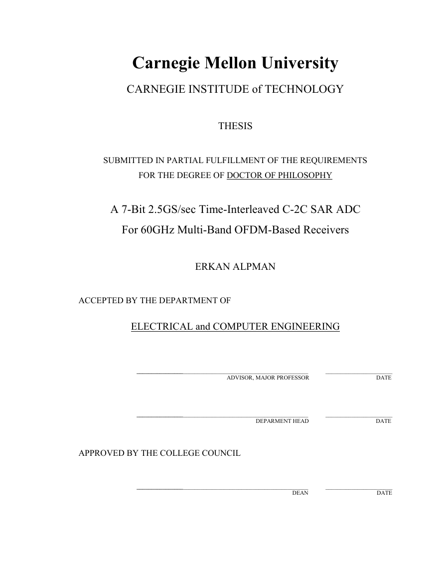
Carnegie Mellon University
CARNEGIE INSTITUDE of TECHNOLOGY
THESIS
SUBMITTED IN PARTIAL FULFILLMENT OF THE REQUIREMENTS
FOR THE DEGREE OF DOCTOR OF PHILOSOPHY
A 7-Bit 2.5GS/sec Time-Interleaved C-2C SAR ADC
For 60GHz Multi-Band OFDM-Based Receivers
ERKAN ALPMAN
ACCEPTED BY THE DEPARTMENT OF
ELECTRICAL and COMPUTER ENGINEERING
___________________________________________________________ _______________________
ADVISOR, MAJOR PROFESSOR DATE
___________________________________________________________ _______________________
DEPARMENT HEAD DATE
APPROVED BY THE COLLEGE COUNCIL
___________________________________________________________ _______________________
DEAN DATE
�
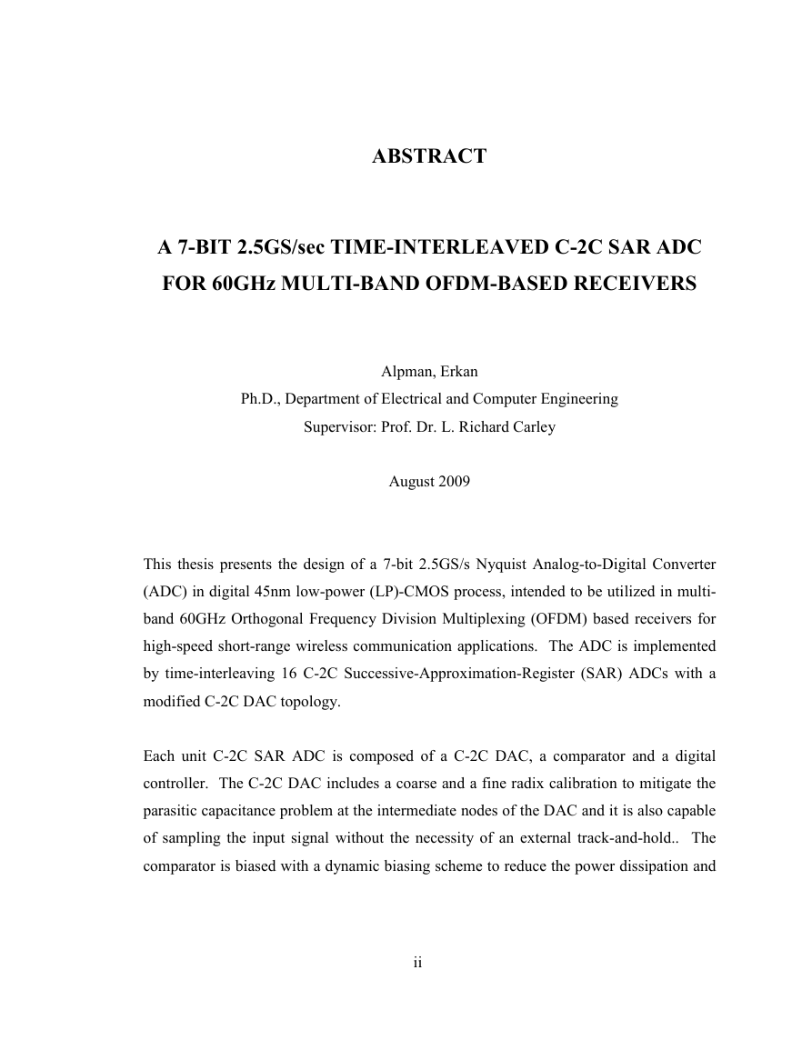
ABSTRACT
A 7-BIT 2.5GS/sec TIME-IҭTERLEAVED C-2C SAR ADC
FOR 60GHz MULTI-BAҭD OFDM-BASED RECEIVERS
Alpman, Erkan
Ph.D., Department of Electrical and Computer Engineering
Supervisor: Prof. Dr. L. Richard Carley
August 2009
This thesis presents the design of a 7-bit 2.5GS/s Nyquist Analog-to-Digital Converter
(ADC) in digital 45nm low-power (LP)-CMOS process, intended to be utilized in multi-
band 60GHz Orthogonal Frequency Division Multiplexing (OFDM) based receivers for
high-speed short-range wireless communication applications. The ADC is implemented
by time-interleaving 16 C-2C Successive-Approximation-Register (SAR) ADCs with a
modified C-2C DAC topology.
Each unit C-2C SAR ADC is composed of a C-2C DAC, a comparator and a digital
controller. The C-2C DAC includes a coarse and a fine radix calibration to mitigate the
parasitic capacitance problem at the intermediate nodes of the DAC and it is also capable
of sampling the input signal without the necessity of an external track-and-hold.. The
comparator is biased with a dynamic biasing scheme to reduce the power dissipation and
ii
�
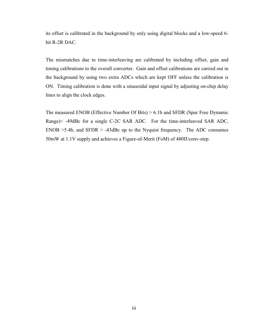
its offset is calibrated in the background by only using digital blocks and a low-speed 6-
bit R-2R DAC.
The mismatches due to time-interleaving are calibrated by including offset, gain and
timing calibrations to the overall converter. Gain and offset calibrations are carried out in
the background by using two extra ADCs which are kept OFF unless the calibration is
ON. Timing calibration is done with a sinusoidal input signal by adjusting on-chip delay
lines to align the clock edges.
The measured ENOB (Effective Number Of Bits) > 6.1b and SFDR (Spur Free Dynamic
Range)< -49dBc for a single C-2C SAR ADC. For the time-interleaved SAR ADC,
ENOB >5.4b, and SFDR > -43dBc up to the Nyquist frequency. The ADC consumes
50mW at 1.1V supply and achieves a Figure-of-Merit (FoM) of 480fJ/conv-step.
iii
�
To My Family
and
To The Memory of My Grandparents
Husnu & Ruvide Alpman and Mithat & Leman Erkut
iv
�
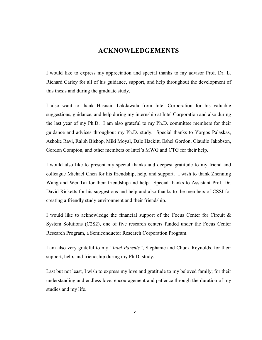
ACKҭOWLEDGEMEҭTS
I would like to express my appreciation and special thanks to my advisor Prof. Dr. L.
Richard Carley for all of his guidance, support, and help throughout the development of
this thesis and during the graduate study.
I also want to thank Hasnain Lakdawala from Intel Corporation for his valuable
suggestions, guidance, and help during my internship at Intel Corporation and also during
the last year of my Ph.D. I am also grateful to my Ph.D. committee members for their
guidance and advices throughout my Ph.D. study. Special thanks to Yorgos Palaskas,
Ashoke Ravi, Ralph Bishop, Miki Moyal, Dale Hackitt, Eshel Gordon, Claudio Jakobson,
Gordon Compton, and other members of Intel’s MWG and CTG for their help.
I would also like to present my special thanks and deepest gratitude to my friend and
colleague Michael Chen for his friendship, help, and support. I wish to thank Zhenning
Wang and Wei Tai for their friendship and help. Special thanks to Assistant Prof. Dr.
David Ricketts for his suggestions and help and also thanks to the members of CSSI for
creating a friendly study environment and their friendship.
I would like to acknowledge the financial support of the Focus Center for Circuit &
System Solutions (C2S2), one of five research centers funded under the Focus Center
Research Program, a Semiconductor Research Corporation Program.
I am also very grateful to my “Intel Parents”, Stephanie and Chuck Reynolds, for their
support, help, and friendship during my Ph.D. study.
Last but not least, I wish to express my love and gratitude to my beloved family; for their
understanding and endless love, encouragement and patience through the duration of my
studies and my life.
v
�
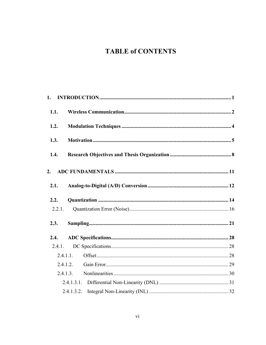
TABLE of COҭTEҭTS
1.
IҭTRODUCTIOҭ..................................................................................................... 1
1.1. Wireless Communication.................................................................................. 2
1.2. Modulation Techniques .................................................................................... 4
1.3. Motivation .......................................................................................................... 5
1.4.
Research Objectives and Thesis Organization ............................................... 8
2. ADC FUҭDAMEҭTALS ....................................................................................... 11
2.1.
Analog-to-Digital (A/D) Conversion .............................................................. 12
2.2.
Quantization .................................................................................................... 14
2.2.1.
Quantization Error (Noise)............................................................................ 16
2.3.
Sampling........................................................................................................... 21
2.4.
ADC Specifications.......................................................................................... 28
2.4.1.
DC Specifications.......................................................................................... 28
2.4.1.1.
2.4.1.2.
2.4.1.3.
Offset..................................................................................................... 28
Gain Error.............................................................................................. 29
Nonlinearities ........................................................................................ 30
2.4.1.3.1. Differential Non-Linearity (DNL) ..................................................... 31
2.4.1.3.2.
Integral Non-Linearity (INL) ............................................................. 32
vi
�
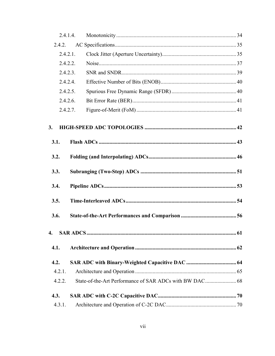
2.4.1.4. Monotonicity ......................................................................................... 34
2.4.2.
AC Specifications.......................................................................................... 35
2.4.2.1.
2.4.2.2.
2.4.2.3.
2.4.2.4.
2.4.2.5.
2.4.2.6.
2.4.2.7.
Clock Jitter (Aperture Uncertainty)....................................................... 35
Noise...................................................................................................... 37
SNR and SNDR..................................................................................... 39
Effective Number of Bits (ENOB)........................................................ 40
Spurious Free Dynamic Range (SFDR) ................................................ 40
Bit Error Rate (BER)............................................................................. 41
Figure-of-Merit (FoM) .......................................................................... 41
3. HIGH-SPEED ADC TOPOLOGIES .................................................................... 42
3.1.
Flash ADCs ...................................................................................................... 43
3.2.
Folding (and Interpolating) ADCs................................................................. 46
3.3.
Subranging (Two-Step) ADCs ....................................................................... 51
3.4.
Pipeline ADCs .................................................................................................. 53
3.5.
Time-Interleaved ADCs.................................................................................. 54
3.6.
State-of-the-Art Performances and Comparison ......................................... 56
4. SAR ADCS ............................................................................................................... 61
4.1.
Architecture and Operation ........................................................................... 62
4.2.
SAR ADC with Binary-Weighted Capacitive DAC ..................................... 64
4.2.1.
4.2.2.
Architecture and Operation ........................................................................... 65
State-of-the-Art Performance of SAR ADCs with BW DAC....................... 68
4.3.
SAR ADC with C-2C Capacitive DAC.......................................................... 70
4.3.1.
Architecture and Operation of C-2C DAC.................................................... 70
vii
�
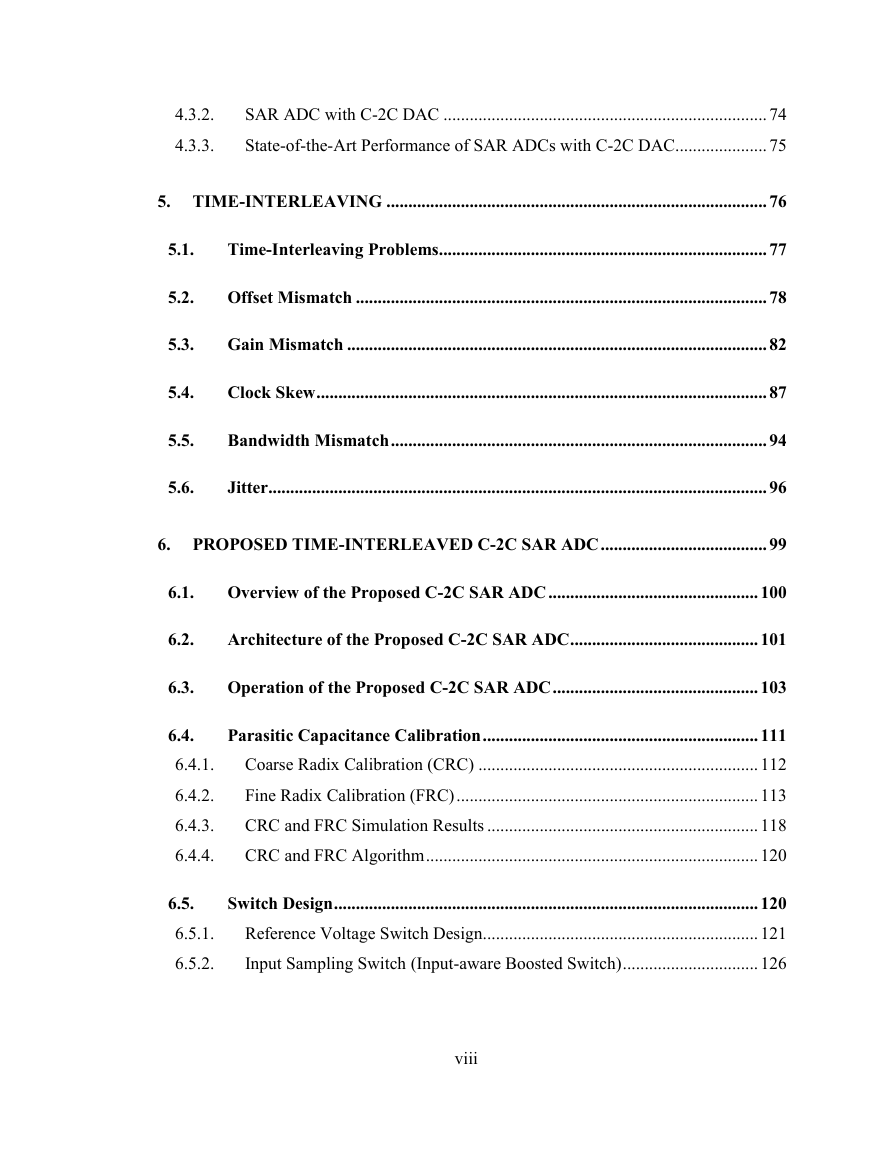
4.3.2.
4.3.3.
SAR ADC with C-2C DAC .......................................................................... 74
State-of-the-Art Performance of SAR ADCs with C-2C DAC..................... 75
5. TIME-IҭTERLEAVIҭG ....................................................................................... 76
5.1.
Time-Interleaving Problems........................................................................... 77
5.2.
Offset Mismatch .............................................................................................. 78
5.3.
Gain Mismatch ................................................................................................ 82
5.4.
Clock Skew....................................................................................................... 87
5.5.
Bandwidth Mismatch...................................................................................... 94
5.6.
Jitter.................................................................................................................. 96
6. PROPOSED TIME-IҭTERLEAVED C-2C SAR ADC ...................................... 99
6.1.
Overview of the Proposed C-2C SAR ADC ................................................ 100
6.2.
Architecture of the Proposed C-2C SAR ADC........................................... 101
6.3.
Operation of the Proposed C-2C SAR ADC ............................................... 103
6.4.
Parasitic Capacitance Calibration............................................................... 111
6.4.1.
6.4.2.
6.4.3.
6.4.4.
Coarse Radix Calibration (CRC) ................................................................ 112
Fine Radix Calibration (FRC)..................................................................... 113
CRC and FRC Simulation Results .............................................................. 118
CRC and FRC Algorithm............................................................................ 120
6.5.
Switch Design................................................................................................. 120
6.5.1.
6.5.2.
Reference Voltage Switch Design............................................................... 121
Input Sampling Switch (Input-aware Boosted Switch)............................... 126
viii
�


 2023年江西萍乡中考道德与法治真题及答案.doc
 2012年重庆南川中考生物真题及答案.doc
 2013年江西师范大学地理学综合及文艺理论基础考研真题.doc
 2020年四川甘孜小升初语文真题及答案I卷.doc
 2020年注册岩土工程师专业基础考试真题及答案.doc
 2023-2024学年福建省厦门市九年级上学期数学月考试题及答案.doc
 2021-2022学年辽宁省沈阳市大东区九年级上学期语文期末试题及答案.doc
 2022-2023学年北京东城区初三第一学期物理期末试卷及答案.doc
 2018上半年江西教师资格初中地理学科知识与教学能力真题及答案.doc
 2012年河北国家公务员申论考试真题及答案-省级.doc
 2020-2021学年江苏省扬州市江都区邵樊片九年级上学期数学第一次质量检测试题及答案.doc
 2022下半年黑龙江教师资格证中学综合素质真题及答案.doc