www.ti.com
SBAS499A –JULY 2012 –REVISED AUGUST 2012
Low-Noise, 8-Channel, 24-Bit Analog Front-End for Biopotential Measurements
Check for Samples: ADS1299
ADS1299
systems
instrumentation
With its high levels of
integration and exceptional
performance, the ADS1299 enables the creation of
scalable medical
at
significantly reduced size, power, and overall cost.
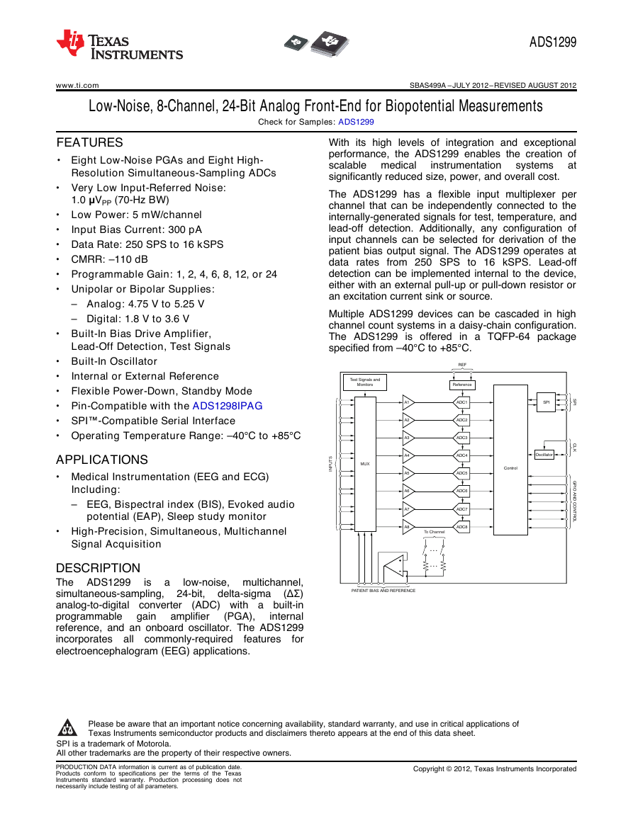
The ADS1299 has a flexible input multiplexer per
channel that can be independently connected to the
internally-generated signals for test, temperature, and
lead-off detection. Additionally, any configuration of
input channels can be selected for derivation of the
patient bias output signal. The ADS1299 operates at
data rates from 250 SPS to 16 kSPS. Lead-off
detection can be implemented internal to the device,
either with an external pull-up or pull-down resistor or
an excitation current sink or source.
Multiple ADS1299 devices can be cascaded in high
channel count systems in a daisy-chain configuration.
The ADS1299 is offered in a TQFP-64 package
specified from –40°C to +85°C.
1FEATURES
23• Eight Low-Noise PGAs and Eight High-
Resolution Simultaneous-Sampling ADCs
• Very Low Input-Referred Noise:
1.0 μVPP (70-Hz BW)
• Low Power: 5 mW/channel
•
Input Bias Current: 300 pA
• Data Rate: 250 SPS to 16 kSPS
• CMRR: –110 dB
• Programmable Gain: 1, 2, 4, 6, 8, 12, or 24
• Unipolar or Bipolar Supplies:
– Analog: 4.75 V to 5.25 V
– Digital: 1.8 V to 3.6 V
• Built-In Bias Drive Amplifier,
Lead-Off Detection, Test Signals
Internal or External Reference
• Built-In Oscillator
•
• Flexible Power-Down, Standby Mode
• Pin-Compatible with the ADS1298IPAG
• SPI™-Compatible Serial Interface
• Operating Temperature Range: –40°C to +85°C
APPLICATIONS
• Medical Instrumentation (EEG and ECG)
Including:
– EEG, Bispectral index (BIS), Evoked audio
potential (EAP), Sleep study monitor
• High-Precision, Simultaneous, Multichannel
Signal Acquisition
DESCRIPTION
low-noise, multichannel,
The ADS1299
(ΔΣ)
simultaneous-sampling,
(ADC) with a built-in
analog-to-digital converter
programmable
internal
reference, and an onboard oscillator. The ADS1299
incorporates all
for
electroencephalogram (EEG) applications.
commonly-required features
delta-sigma
amplifier
(PGA),
is
a
24-bit,
gain
1
Please be aware that an important notice concerning availability, standard warranty, and use in critical applications of
Texas Instruments semiconductor products and disclaimers thereto appears at the end of this data sheet.
2SPI is a trademark of Motorola.
3All other trademarks are the property of their respective owners.
PRODUCTION DATA information is current as of publication date.
Products conform to specifications per the terms of
the Texas
Instruments standard warranty. Production processing does not
necessarily include testing of all parameters.
Copyright © 2012, Texas Instruments Incorporated
ControlCLKGPIO AND CONTROLOscillatorSPITest Signals andMonitorsSPIPATIENT BIAS AND REFERENCEReferenceREFADC7ADC8ADC1ADC2ADC3ADC4ADC5ADC6A7A8A1A2A3A4A5A6MUXINPUTS¼¼To Channel�
ADS1299
SBAS499A –JULY 2012–REVISED AUGUST 2012
www.ti.com
This integrated circuit can be damaged by ESD. Texas Instruments recommends that all
appropriate precautions. Failure to observe proper handling and installation procedures can cause damage.
integrated circuits be handled with
ESD damage can range from subtle performance degradation to complete device failure. Precision integrated circuits may be more
susceptible to damage because very small parametric changes could cause the device not to meet its published specifications.
FAMILY AND ORDERING INFORMATION(1)
PRODUCT
PACKAGE OPTION
ADS1299IPAG
TQFP
NUMBER OF
CHANNELS
8
ADC RESOLUTION
MAXIMUM SAMPLE
RATE (kSPS)
OPERATING
TEMPERATURE
RANGE
24
16
–40°C to +85°C
(1) For the most current package and ordering information, see the Package Option Addendum at the end of this document, or visit the
device product folder at www.ti.com.
ABSOLUTE MAXIMUM RATINGS(1)
Over operating free-air temperature range, unless otherwise noted.
AVDD to AVSS
DVDD to DGND
AVSS to DGND
VREF input to AVSS
Analog input to AVSS
Digital input voltage to DGND
Digital output voltage to DGND
Momentary
Continuous
Operating range, TA
Storage range, Tstg
Maximum junction, TJ
Human body model (HBM)
JEDEC standard 22, test method A114-C.01, all pins
Charged device model (CDM)
JEDEC standard 22, test method C101, all pins
Electrostatic
discharge (ESD)
ratings
Temperature
Input current
VALUE
–0.3 to +5.5
–0.3 to +3.9
–3 to +0.2
AVSS – 0.3 to AVDD + 0.3
AVSS – 0.3 to AVDD + 0.3
–0.3 to DVDD + 0.3
–0.3 to DVDD + 0.3
100
10
–40 to +85
–60 to +150
+150
±1000
±500
UNIT
V
V
V
V
V
V
V
mA
mA
°C
°C
°C
V
V
(1) Stresses above these ratings may cause permanent damage. Exposure to absolute maximum conditions for extended periods may
degrade device reliability. These are stress ratings only, and functional operation of the device at these or any other conditions beyond
those specified is not implied.
2
Copyright © 2012, Texas Instruments Incorporated
�
ADS1299
www.ti.com
SBAS499A –JULY 2012 –REVISED AUGUST 2012
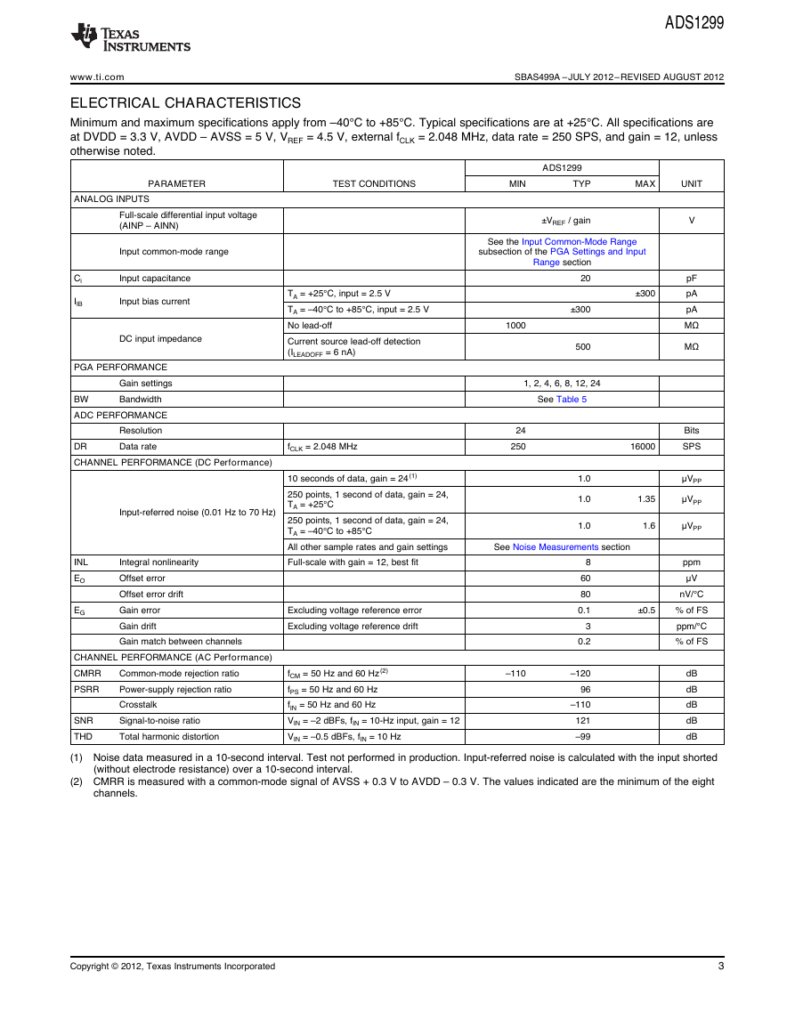
ELECTRICAL CHARACTERISTICS
Minimum and maximum specifications apply from –40°C to +85°C. Typical specifications are at +25°C. All specifications are
at DVDD = 3.3 V, AVDD – AVSS = 5 V, VREF = 4.5 V, external fCLK = 2.048 MHz, data rate = 250 SPS, and gain = 12, unless
otherwise noted.
PARAMETER
TEST CONDITIONS
MIN
TYP
MAX
UNIT
ADS1299
ANALOG INPUTS
Full-scale differential input voltage
(AINP – AINN)
Input common-mode range
Ci
IIB
Input capacitance
Input bias current
DC input impedance
PGA PERFORMANCE
Gain settings
Bandwidth
BW
ADC PERFORMANCE
Resolution
TA = +25°C, input = 2.5 V
TA = –40°C to +85°C, input = 2.5 V
No lead-off
Current source lead-off detection
(ILEADOFF = 6 nA)
Data rate
DR
CHANNEL PERFORMANCE (DC Performance)
fCLK = 2.048 MHz
Input-referred noise (0.01 Hz to 70 Hz)
INL
EO
EG
Integral nonlinearity
Offset error
Offset error drift
Gain error
Gain drift
Gain match between channels
CHANNEL PERFORMANCE (AC Performance)
CMRR
Common-mode rejection ratio
PSRR
Power-supply rejection ratio
Crosstalk
SNR
THD
Signal-to-noise ratio
Total harmonic distortion
10 seconds of data, gain = 24 (1)
250 points, 1 second of data, gain = 24,
TA = +25°C
250 points, 1 second of data, gain = 24,
TA = –40°C to +85°C
All other sample rates and gain settings
Full-scale with gain = 12, best fit
Excluding voltage reference error
Excluding voltage reference drift
fCM = 50 Hz and 60 Hz (2)
fPS = 50 Hz and 60 Hz
fIN = 50 Hz and 60 Hz
VIN = –2 dBFs, fIN = 10-Hz input, gain = 12
VIN = –0.5 dBFs, fIN = 10 Hz
–110
±VREF / gain
See the Input Common-Mode Range
subsection of the PGA Settings and Input
Range section
20
±300
500
1000
1, 2, 4, 6, 8, 12, 24
See Table 5
24
250
1.0
1.0
1.0
See Noise Measurements section
±300
16000
1.35
1.6
±0.5
8
60
80
0.1
3
0.2
–120
96
–110
121
–99
V
pF
pA
pA
MΩ
MΩ
Bits
SPS
μVPP
μVPP
μVPP
ppm
μV
nV/°C
% of FS
ppm/°C
% of FS
dB
dB
dB
dB
dB
(1) Noise data measured in a 10-second interval. Test not performed in production. Input-referred noise is calculated with the input shorted
(without electrode resistance) over a 10-second interval.
(2) CMRR is measured with a common-mode signal of AVSS + 0.3 V to AVDD – 0.3 V. The values indicated are the minimum of the eight
channels.
Copyright © 2012, Texas Instruments Incorporated
3
�
ADS1299
SBAS499A –JULY 2012–REVISED AUGUST 2012
www.ti.com
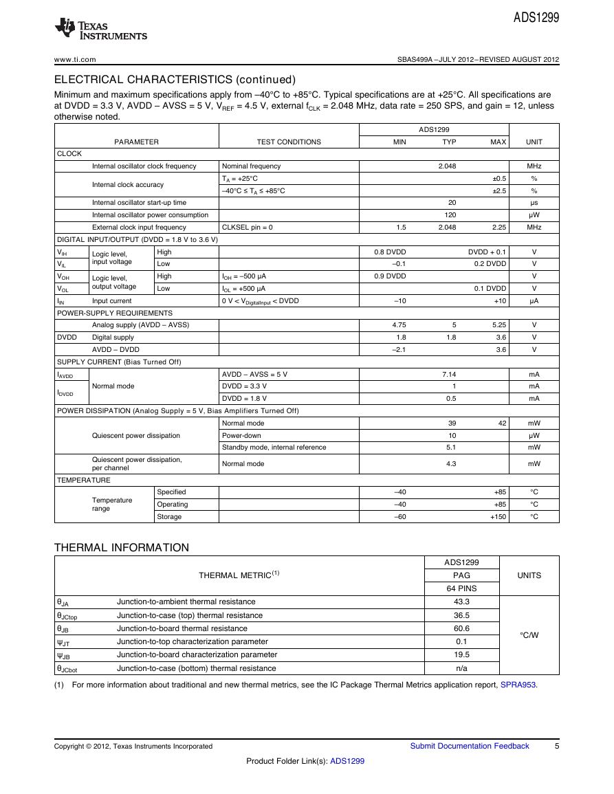
ELECTRICAL CHARACTERISTICS (continued)
Minimum and maximum specifications apply from –40°C to +85°C. Typical specifications are at +25°C. All specifications are
at DVDD = 3.3 V, AVDD – AVSS = 5 V, VREF = 4.5 V, external fCLK = 2.048 MHz, data rate = 250 SPS, and gain = 12, unless
otherwise noted.
PARAMETER
TEST CONDITIONS
MIN
PATIENT BIAS AMPLIFIER
Integrated noise
GBP
SR
THD
CMIR
ISC
Gain bandwidth product
Slew rate
Total harmonic distortion
Common-mode input range
Short-circuit current
Quiescent power consumption
LEAD-OFF DETECT
BW = 150 Hz
50 kΩ || 10 pF load, gain = 1
50 kΩ || 10 pF load, gain = 1
fIN = 10 Hz, gain = 1
AVSS + 0.3
ADS1299
TYP
2
100
0.07
–80
1.1
20
Frequency
Current
Current accuracy
Comparator threshold accuracy
Continuous
One time or periodic
ILEAD_OFF[1:0] = 00
ILEAD_OFF[1:0] = 01
ILEAD_OFF[1:0] = 10
ILEAD_OFF[1:0] = 11
EXTERNAL REFERENCE
VI(ref)
VREFN
Negative input
Reference input voltage
VREFP
Positive input
Input impedance
INTERNAL REFERENCE
Output voltage
VO
VREF accuracy
Drift
Start-up time
SYSTEM MONITORS
5-V supply, VREF = (VREFP – VREFN)
TA = –40°C to +85°C
Analog supply
Digital supply
Reading error
Device wake up
Temperature
sensor reading
Voltage
Coefficient
From power-up to DRDY low
STANDBY mode
TA = +25°C
0, fDR / 4
See Register Map section for settings
7.8, 31.2
6
24
6
24
±20
±30
4.5
AVSS
AVSS + 4.5
5.6
4.5
±0.2
35
150
2
2
150
31.25
145
490
Signal frequency
See Register Map section for settings
Test signal
Signal voltage
See Register Map section for settings
Accuracy
fCLK / 221, fCLK / 220
±1, ±2
±2
MAX
UNIT
AVDD – 0.3
μVRMS
kHz
V/μs
dB
V
mA
μA
Hz
Hz
nA
nA
μA
μA
%
mV
V
V
V
kΩ
V
%
ppm
ms
%
%
ms
µs
mV
μV/°C
Hz
mV
%
4
Copyright © 2012, Texas Instruments Incorporated
�
ADS1299
www.ti.com
SBAS499A –JULY 2012 –REVISED AUGUST 2012
ELECTRICAL CHARACTERISTICS (continued)
Minimum and maximum specifications apply from –40°C to +85°C. Typical specifications are at +25°C. All specifications are
at DVDD = 3.3 V, AVDD – AVSS = 5 V, VREF = 4.5 V, external fCLK = 2.048 MHz, data rate = 250 SPS, and gain = 12, unless
otherwise noted.
PARAMETER
TEST CONDITIONS
MIN
TYP
MAX
UNIT
ADS1299
CLOCK
Internal oscillator clock frequency
Internal clock accuracy
Internal oscillator start-up time
Internal oscillator power consumption
Nominal frequency
TA = +25°C
–40°C ≤ TA ≤ +85°C
External clock input frequency
CLKSEL pin = 0
Logic level,
input voltage
DIGITAL INPUT/OUTPUT (DVDD = 1.8 V to 3.6 V)
VIH
VIL
VOH
VOL
IIN
POWER-SUPPLY REQUIREMENTS
Logic level,
output voltage
Input current
High
Low
High
Low
Analog supply (AVDD – AVSS)
DVDD
Digital supply
AVDD – DVDD
SUPPLY CURRENT (Bias Turned Off)
IAVDD
Normal mode
IDVDD
IOH = –500 μA
IOL = +500 μA
0 V < VDigitalInput < DVDD
AVDD – AVSS = 5 V
DVDD = 3.3 V
DVDD = 1.8 V
POWER DISSIPATION (Analog Supply = 5 V, Bias Amplifiers Turned Off)
Quiescent power dissipation
Normal mode
Power-down
Standby mode, internal reference
Quiescent power dissipation,
per channel
Normal mode
TEMPERATURE
Temperature
range
Specified
Operating
Storage
THERMAL INFORMATION
THERMAL METRIC(1)
θJA
θJCtop
θJB
ψJT
ψJB
θJCbot
Junction-to-ambient thermal resistance
Junction-to-case (top) thermal resistance
Junction-to-board thermal resistance
Junction-to-top characterization parameter
Junction-to-board characterization parameter
Junction-to-case (bottom) thermal resistance
1.5
0.8 DVDD
–0.1
0.9 DVDD
–10
4.75
1.8
–2.1
–40
–40
–60
MHz
%
%
μs
μW
MHz
V
V
V
V
μA
V
V
V
mA
mA
mA
mW
μW
mW
mW
°C
°C
°C
UNITS
°C/W
2.048
20
120
2.048
5
1.8
7.14
1
0.5
39
10
5.1
4.3
±0.5
±2.5
2.25
DVDD + 0.1
0.2 DVDD
0.1 DVDD
+10
5.25
3.6
3.6
42
+85
+85
+150
ADS1299
PAG
64 PINS
43.3
36.5
60.6
0.1
19.5
n/a
(1) For more information about traditional and new thermal metrics, see the IC Package Thermal Metrics application report, SPRA953.
Copyright © 2012, Texas Instruments Incorporated
Submit Documentation Feedback
5
Product Folder Link(s): ADS1299
�
ADS1299
SBAS499A –JULY 2012–REVISED AUGUST 2012
www.ti.com
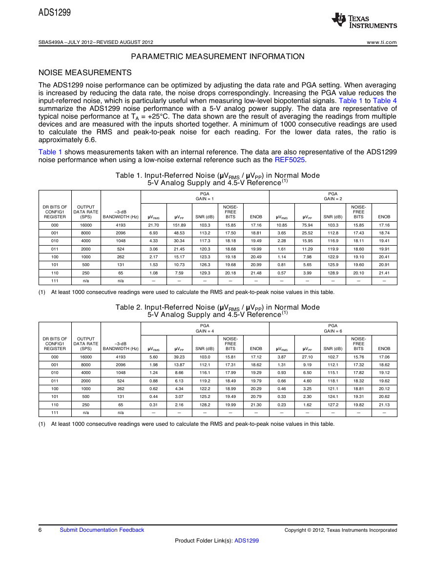
PARAMETRIC MEASUREMENT INFORMATION
NOISE MEASUREMENTS
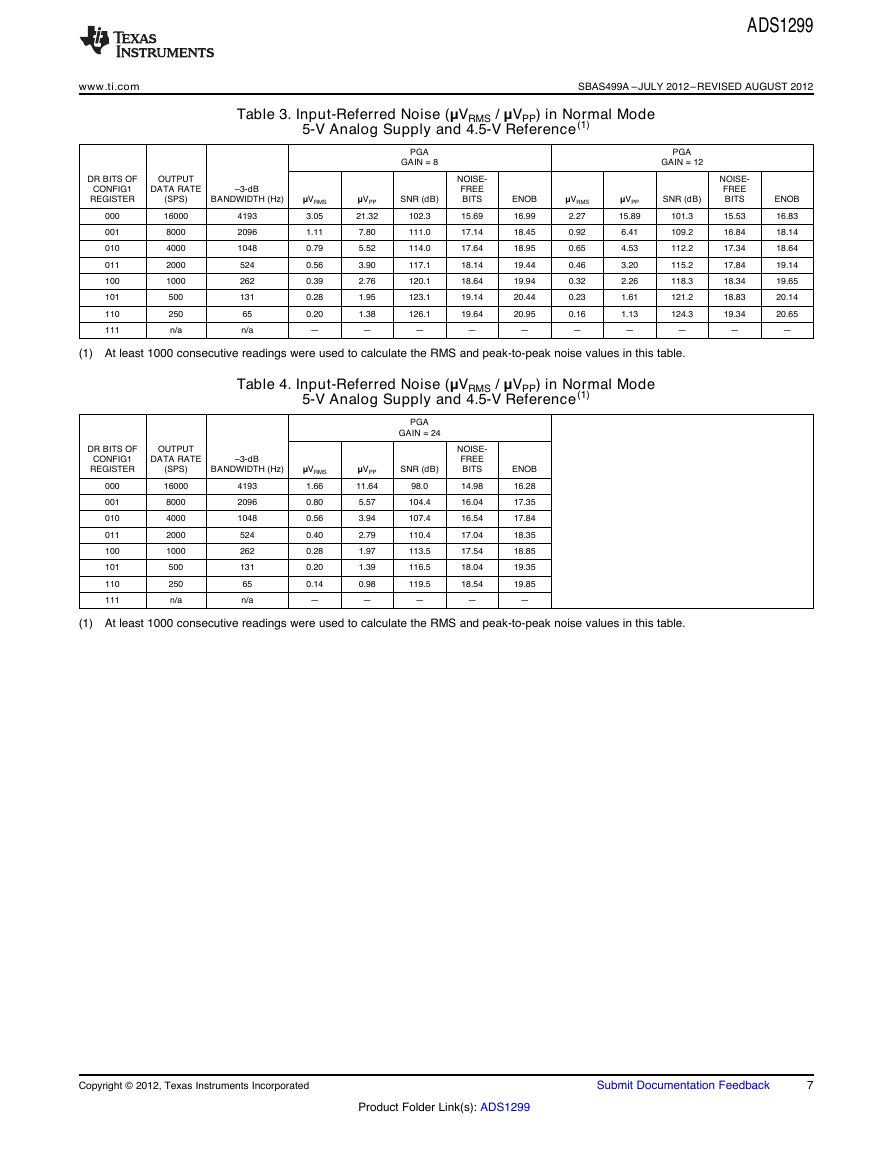
The ADS1299 noise performance can be optimized by adjusting the data rate and PGA setting. When averaging
is increased by reducing the data rate, the noise drops correspondingly. Increasing the PGA value reduces the
input-referred noise, which is particularly useful when measuring low-level biopotential signals. Table 1 to Table 4
summarize the ADS1299 noise performance with a 5-V analog power supply. The data are representative of
typical noise performance at TA = +25°C. The data shown are the result of averaging the readings from multiple
devices and are measured with the inputs shorted together. A minimum of 1000 consecutive readings are used
to calculate the RMS and peak-to-peak noise for each reading. For the lower data rates,
the ratio is
approximately 6.6.
Table 1 shows measurements taken with an internal reference. The data are also representative of the ADS1299
noise performance when using a low-noise external reference such as the REF5025.
Table 1. Input-Referred Noise (μVRMS / μVPP) in Normal Mode
5-V Analog Supply and 4.5-V Reference(1)
DR BITS OF
CONFIG1
REGISTER
000
001
010
011
100
101
110
111
OUTPUT
DATA RATE
(SPS)
–3-dB
BANDWIDTH (Hz)
16000
8000
4000
2000
1000
500
250
n/a
4193
2096
1048
524
262
131
65
n/a
PGA
GAIN = 1
SNR (dB)
103.3
113.2
117.3
120.3
123.3
126.3
129.3
—
NOISE-
FREE
BITS
15.85
17.50
18.18
18.68
19.18
19.68
20.18
—
μVRMS
21.70
6.93
4.33
3.06
2.17
1.53
1.08
—
μVPP
151.89
48.53
30.34
21.45
15.17
10.73
7.59
—
ENOB
17.16
18.81
19.49
19.99
20.49
20.99
21.48
—
μVRMS
10.85
3.65
2.28
1.61
1.14
0.81
0.57
—
μVPP
75.94
25.52
15.95
11.29
7.98
5.65
3.99
—
PGA
GAIN = 2
SNR (dB)
103.3
112.8
116.9
119.9
122.9
125.9
128.9
—
(1) At least 1000 consecutive readings were used to calculate the RMS and peak-to-peak noise values in this table.
Table 2. Input-Referred Noise (μVRMS / μVPP) in Normal Mode
5-V Analog Supply and 4.5-V Reference(1)
DR BITS OF
CONFIG1
REGISTER
000
001
010
011
100
101
110
111
OUTPUT
DATA RATE
(SPS)
–3-dB
BANDWIDTH (Hz)
16000
8000
4000
2000
1000
500
250
n/a
4193
2096
1048
524
262
131
65
n/a
PGA
GAIN = 4
SNR (dB)
103.0
112.1
116.1
119.2
122.2
125.2
128.2
—
NOISE-
FREE
BITS
15.81
17.31
17.99
18.49
18.99
19.49
19.99
—
μVRMS
5.60
1.98
1.24
0.88
0.62
0.44
0.31
—
μVPP
39.23
13.87
8.66
6.13
4.34
3.07
2.16
—
ENOB
17.12
18.62
19.29
19.79
20.29
20.79
21.30
—
μVRMS
3.87
1.31
0.93
0.66
0.46
0.33
0.23
—
μVPP
27.10
9.19
6.50
4.60
3.25
2.30
1.62
—
PGA
GAIN = 6
SNR (dB)
102.7
112.1
115.1
118.1
121.1
124.1
127.2
—
NOISE-
FREE
BITS
15.85
17.43
18.11
18.60
19.10
19.60
20.10
—
NOISE-
FREE
BITS
15.76
17.32
17.82
18.32
18.81
19.31
19.82
—
ENOB
17.16
18.74
19.41
19.91
20.41
20.91
21.41
—
ENOB
17.06
18.62
19.12
19.62
20.12
20.62
21.13
—
(1) At least 1000 consecutive readings were used to calculate the RMS and peak-to-peak noise values in this table.
6
Submit Documentation Feedback
Copyright © 2012, Texas Instruments Incorporated
Product Folder Link(s): ADS1299
�
www.ti.com
SBAS499A –JULY 2012 –REVISED AUGUST 2012
Table 3. Input-Referred Noise (μVRMS / μVPP) in Normal Mode
5-V Analog Supply and 4.5-V Reference(1)
ADS1299
DR BITS OF
CONFIG1
REGISTER
000
001
010
011
100
101
110
111
OUTPUT
DATA RATE
(SPS)
–3-dB
BANDWIDTH (Hz)
16000
8000
4000
2000
1000
500
250
n/a
4193
2096
1048
524
262
131
65
n/a
PGA
GAIN = 8
SNR (dB)
102.3
111.0
114.0
117.1
120.1
123.1
126.1
—
NOISE-
FREE
BITS
15.69
17.14
17.64
18.14
18.64
19.14
19.64
—
μVRMS
3.05
1.11
0.79
0.56
0.39
0.28
0.20
—
μVPP
21.32
7.80
5.52
3.90
2.76
1.95
1.38
—
ENOB
16.99
18.45
18.95
19.44
19.94
20.44
20.95
—
μVRMS
2.27
0.92
0.65
0.46
0.32
0.23
0.16
—
μVPP
15.89
6.41
4.53
3.20
2.26
1.61
1.13
—
PGA
GAIN = 12
SNR (dB)
101.3
109.2
112.2
115.2
118.3
121.2
124.3
—
NOISE-
FREE
BITS
15.53
16.84
17.34
17.84
18.34
18.83
19.34
—
ENOB
16.83
18.14
18.64
19.14
19.65
20.14
20.65
—
(1) At least 1000 consecutive readings were used to calculate the RMS and peak-to-peak noise values in this table.
Table 4. Input-Referred Noise (μVRMS / μVPP) in Normal Mode
5-V Analog Supply and 4.5-V Reference(1)
DR BITS OF
CONFIG1
REGISTER
000
001
010
011
100
101
110
111
OUTPUT
DATA RATE
(SPS)
–3-dB
BANDWIDTH (Hz)
16000
8000
4000
2000
1000
500
250
n/a
4193
2096
1048
524
262
131
65
n/a
PGA
GAIN = 24
SNR (dB)
98.0
104.4
107.4
110.4
113.5
116.5
119.5
—
NOISE-
FREE
BITS
14.98
16.04
16.54
17.04
17.54
18.04
18.54
—
ENOB
16.28
17.35
17.84
18.35
18.85
19.35
19.85
—
μVRMS
1.66
0.80
0.56
0.40
0.28
0.20
0.14
—
μVPP
11.64
5.57
3.94
2.79
1.97
1.39
0.98
—
(1) At least 1000 consecutive readings were used to calculate the RMS and peak-to-peak noise values in this table.
Copyright © 2012, Texas Instruments Incorporated
Submit Documentation Feedback
7
Product Folder Link(s): ADS1299
�
ADS1299
SBAS499A –JULY 2012–REVISED AUGUST 2012
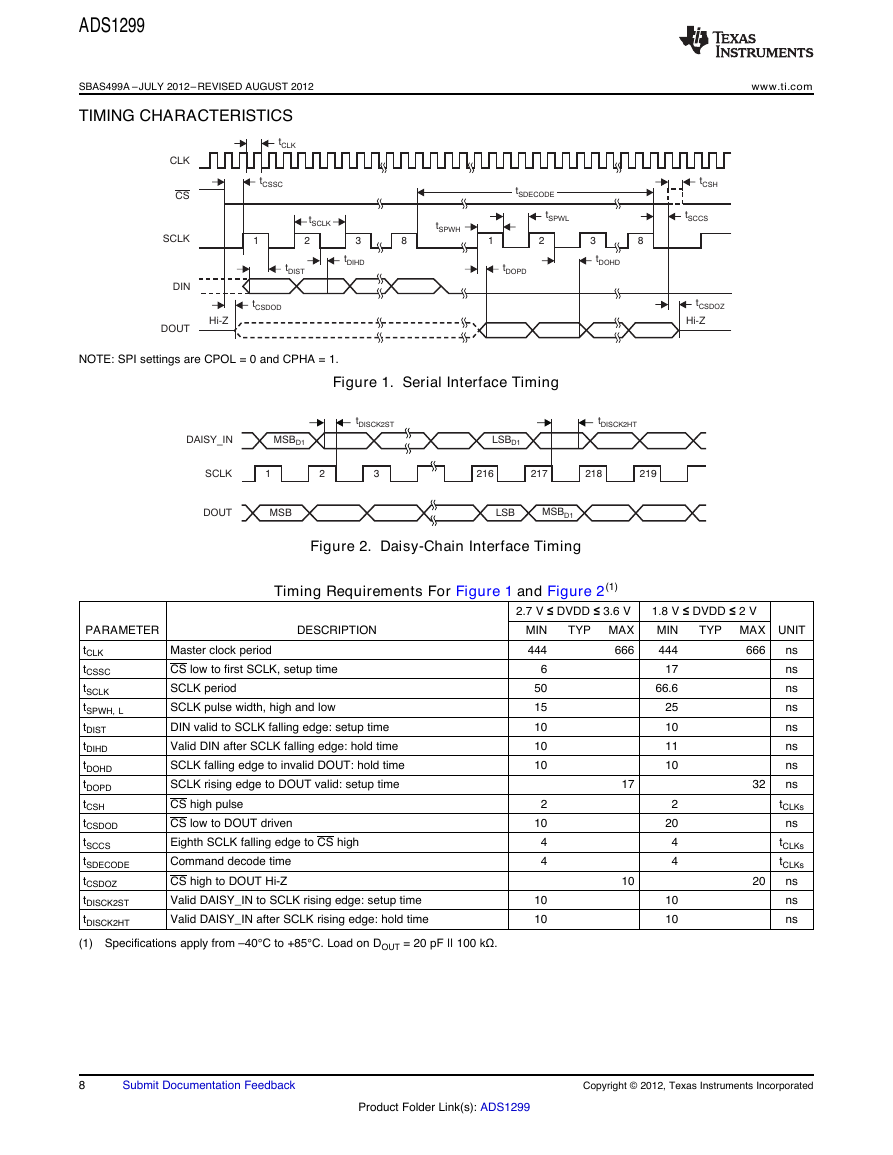
TIMING CHARACTERISTICS
www.ti.com
NOTE: SPI settings are CPOL = 0 and CPHA = 1.
Figure 1. Serial Interface Timing
Figure 2. Daisy-Chain Interface Timing
Timing Requirements For Figure 1 and Figure 2(1)
DESCRIPTION
PARAMETER
tCLK
tCSSC
tSCLK
tSPWH, L
tDIST
tDIHD
tDOHD
tDOPD
tCSH
tCSDOD
tSCCS
tSDECODE
tCSDOZ
tDISCK2ST
tDISCK2HT
(1) Specifications apply from –40°C to +85°C. Load on DOUT = 20 pF || 100 kΩ.
Master clock period
CS low to first SCLK, setup time
SCLK period
SCLK pulse width, high and low
DIN valid to SCLK falling edge: setup time
Valid DIN after SCLK falling edge: hold time
SCLK falling edge to invalid DOUT: hold time
SCLK rising edge to DOUT valid: setup time
CS high pulse
CS low to DOUT driven
Eighth SCLK falling edge to CS high
Command decode time
CS high to DOUT Hi-Z
Valid DAISY_IN to SCLK rising edge: setup time
Valid DAISY_IN after SCLK rising edge: hold time
2.7 V ≤ DVDD ≤ 3.6 V
TYP MAX
666
MIN
444
6
50
15
10
10
10
666
1.8 V ≤ DVDD ≤ 2 V
MIN
444
17
66.6
25
10
11
10
TYP MAX UNIT
ns
ns
ns
ns
ns
ns
ns
ns
tCLKs
ns
tCLKs
tCLKs
ns
ns
ns
2
10
4
4
10
10
17
10
2
20
4
4
10
10
32
20
8
Submit Documentation Feedback
Copyright © 2012, Texas Instruments Incorporated
Product Folder Link(s): ADS1299
DISY_INADOUTSCLKMSBD1tDISCK2STMSB213216217218MSBD1LSBtDISCK2HTLSBD12191CSSCLKDINDOUT2381283tCSSCtDISTtDIHDtDOHDtCSHtDOPDtSPWHtSPWLtSCCSHi-ZtCSDOZtCSDODHi-ZtSCLKtSDECODECLKtCLK�




 2023年江西萍乡中考道德与法治真题及答案.doc
 2012年重庆南川中考生物真题及答案.doc
 2013年江西师范大学地理学综合及文艺理论基础考研真题.doc
 2020年四川甘孜小升初语文真题及答案I卷.doc
 2020年注册岩土工程师专业基础考试真题及答案.doc
 2023-2024学年福建省厦门市九年级上学期数学月考试题及答案.doc
 2021-2022学年辽宁省沈阳市大东区九年级上学期语文期末试题及答案.doc
 2022-2023学年北京东城区初三第一学期物理期末试卷及答案.doc
 2018上半年江西教师资格初中地理学科知识与教学能力真题及答案.doc
 2012年河北国家公务员申论考试真题及答案-省级.doc
 2020-2021学年江苏省扬州市江都区邵樊片九年级上学期数学第一次质量检测试题及答案.doc
 2022下半年黑龙江教师资格证中学综合素质真题及答案.doc