logo资料库

数电基础 Digital Fundamentals, 11_e - Thomas L. Floyd.pdf

第1页 / 共913页
第2页 / 共913页
第3页 / 共913页
第4页 / 共913页
第5页 / 共913页
第6页 / 共913页
第7页 / 共913页
第8页 / 共913页
资料共913页,剩余部分请下载后查看
Cover
Title Page
Copyright Page
PREFACE
Acknowledgments
CONTENTS
CHAPTER 1 Introductory Concepts
1-1 Digital and Analog Quantities
1-2 Binary Digits, Logic Levels, and Digital Waveforms
1-3 Basic Logic Functions
1-4 Combinational and Sequential Logic Functions
1-5 Introduction to Programmable Logic
1-6 Fixed-Function Logic Devices
1-7 Test and Measurement Instruments
1-8 Introduction to Troubleshooting
CHAPTER 2 Number Systems, Operations, and Codes
2-1 Decimal Numbers
2-2 Binary Numbers
2-3 Decimal-to-Binary Conversion
2-4 Binary Arithmetic
2-5 Complements of Binary Numbers
2-6 Signed Numbers
2-7 Arithmetic Operations with Signed Numbers
2-8 Hexadecimal Numbers
2-9 Octal Numbers
2-10 Binary Coded Decimal (BCD)
2-11 Digital Codes
2-12 Error Codes
CHAPTER 3 Logic Gates
3-1 The Inverter
3-2 The AND Gate
3-3 The OR Gate
3-4 The NAND Gate
3-5 The NOR Gate
3-6 The Exclusive-OR and Exclusive-NOR Gates
3-7 Programmable Logic
3-8 Fixed-Function Logic Gates
3-9 Troubleshooting
CHAPTER 4 Boolean Algebra and Logic Simplification
4-1 Boolean Operations and Expressions
4-2 Laws and Rules of Boolean Algebra
4-3 DeMorgan's Theorems
4-4 Boolean Analysis of Logic Circuits
4-5 Logic Simplification Using Boolean Algebra
4-6 Standard Forms of Boolean Expressions
4-7 Boolean Expressions and Truth Tables
4-8 The Karnaugh Map
4-9 Karnaugh Map SOP Minimization
4-10 Karnaugh Map POS Minimization
4-11 The Quine-McCluskey Method
4-12 Boolean Expressions with VHDL
Applied Logic
CHAPTER 5 Combinational Logic Analysis
5-1 Basic Combinational Logic Circuits
5-2 Implementing Combinational Logic
5-3 The Universal Property of NAND and NOR gates
5-4 Combinational Logic Using NAND and NOR Gates
5-5 Pulse Waveform Operation
5-6 Combinational Logic with VHDL
5-7 Troubleshooting
Applied Logic
CHAPTER 6 Functions of Combinational Logic
6-1 Half and Full Adders
6-2 Parallel Binary Adders
6-3 Ripple Carry and Look-Ahead Carry Adders
6-4 Comparators
6-5 Decoders
6-6 Encoders
6-7 Code Converters
6-8 Multiplexers (Data Selectors)
6-9 Demultiplexers
6-10 Parity Generators/Checkers
6-11 Troubleshooting
Applied Logic
CHAPTER 7 Latches, Flip-Flops, and Timers
7-1 Latches
7-2 Flip-Flops
7-3 Flip-Flop Operating Characteristics
7-4 Flip-Flop Applications
7-5 One-Shots
7-6 The Astable Multivibrator
7-7 Troubleshooting
Applied Logic
CHAPTER 8 Shift Registers
8-1 Shift Register Operations
8-2 Types of Shift Register Data I/Os
8-3 Bidirectional Shift Registers
8-4 Shift Register Counters
8-5 Shift Register Applications
8-6 Logic Symbols with Dependency Notation
8-7 Troubleshooting
Applied Logic
CHAPTER 9 Counters
9-1 Finite State Machines
9-2 Asynchronous Counters
9-3 Synchronous Counters
9-4 Up/Down Synchronous Counters
9-5 Design of Synchronous Counters
9-6 Cascaded Counters
9-7 Counter Decoding
9-8 Counter Applications
9-9 Logic Symbols with Dependency Notation
9-10 Troubleshooting
Applied Logic
CHAPTER 10 Programmable Logic
10-1 Simple Programmable Logic Devices (SPLDs)
10-2 Complex Programmable Logic Devices (CPLDs)
10-3 Macrocell Modes
10-4 Field-Programmable Gate Arrays (FPGAs)
10-5 Programmable Logic software
10-6 Boundary Scan Logic
10-7 Troubleshooting
Applied Logic
CHAPTER 11 Data Storage
11-1 Semiconductor Memory Basics
11-2 The Random-Access Memory (RAM)
11-3 The Read-Only Memory (ROM)
11-4 Programmable ROMs
11-5 The Flash Memory
11-6 Memory Expansion
11-7 Special Types of Memories
11-8 Magnetic and Optical Storage
11-9 Memory Hierarchy
11-10 Cloud Storage
11-11 Troubleshooting
CHAPTER 12 Signal Conversion and Processing
12-1 Analog-to-Digital Conversion
12-2 Methods of Analog-to-Digital Conversion
12-3 Methods of Digital-to-Analog Conversion
12-4 Digital Signal Processing
12-5 The Digital Signal Processor (DSP)
CHAPTER 13 Data Transmission
13-1 Data Transmission Media
13-2 Methods and Modes of Data Transmission
13-3 Modulation of Analog Signals with Digital Data
13-4 Modulation of Digital Signals with Analog Data
13-5 Multiplexing and Demultiplexing
13-6 Bus Basics
13-7 Parallel Buses
13-8 The Universal Serial Bus (USB)
13-9 Other Serial Buses
13-10 Bus Interfacing
CHAPTER 14 Data Processing and Control
14-1 The Computer System
14-2 Practical Computer System Considerations
14-3 The Processor: Basic Operation
14-4 The Processor: Addressing Modes
14-5 The Processor: Special Operations
14-6 Operating Systems and Hardware
14-7 Programming
14-8 Microcontrollers and Embedded Systems
14-9 System on Chip (SoC)
ANSWERS TO ODD-NUMBERED PROBLEMS
GLOSSARY
A
B
C
D
E
F
G
H
I
J
K
L
M
N
O
P
Q
R
S
T
U
V
W
Z
INDEX
A
B
C
D
E
F
G
H
I
J
K
L
M
N
O
P
Q
R
S
T
U
V
W
X
Z
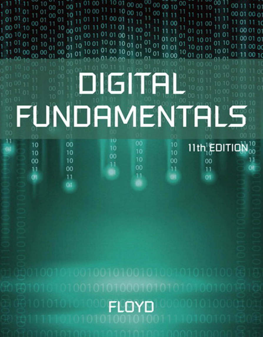
Eleventh Edition Digital Fundamentals Thomas L. Floyd Boston Columbus Indianapolis New York San Francisco Hoboken Amsterdam Cape Town Dubai London Madrid Milan Munich Paris Montreal Toronto Delhi Mexico City São Paulo Sydney Hong Kong Seoul Singapore Taipei Tokyo
Product Manager: Lindsey Prudhomme Gill Program Manager: Maren Beckman Project Manager: Rex Davidson Editorial Assistant: Nancy Kesterson Team Lead Program Manager: Laura Weaver Team Lead Project Manager: JoEllen Gohr Director of Marketing: David Gesell Senior Marketing Coordinator: Stacey Martinez Senior Marketing Assistant: Les Roberts Procurement Specialist: Deidra M. Skahill Media Project Manager: Noelle Chun Media Project Coordinator: April Cleland Creative Director: Andrea Nix Art Director: Diane Y. Ernsberger Cover Designer: Cenveo Publisher Services Cover Image: Hamara/Shutterstock.com Full-Service Project Management: Sherrill Redd/iEnergizer Aptara®, Inc. Composition: iEnergizer Aptara®, Inc. Printer/Binder: R.R. Donnelley & Sons/Willard Cover Printer: Phoenix Color Hagerstown Text Font: Times Roman Credits and acknowledgments for materials borrowed from other sources and reproduced, with permission, in this textbook appear on the appropriate page within text. Copyright © 2015 by Pearson Education, Inc. or its Affiliates. All rights reserved. Manufactured in the United States of America. This publication is protected by Copyright, and permission should be obtained from the publisher prior to any prohibited reproduction, storage in a retrieval system, or transmission in any form or by any means, electronic, mechanical, photocopying, recording, or likewise. To obtain permission(s) to use material from this work, please submit a written request to Pearson Education, Inc., Permissions Department, 221 River Street, Hoboken, New Jersey, 07030. Many of the designations by manufacturers and sellers to distinguish their products are claimed as trademarks. Where those designations appear in this book, and the publisher was aware of a trademark claim, the designations have been printed in initial caps or all caps. Library of Congress Cataloging-in-Publication Data Floyd, Thomas L. Digital fundamentals / Thomas L. Floyd.—Eleventh edition. pages cm ISBN 978-0-13-273796-8 (0-13-273796-5) 1. Digital electronics. 2. Logic circuits. TK7868.D5F53 2015 621.381—dc23 I. Title. 2014017765 10 9 8 7 6 5 4 3 2 1 0-13-273796-5 ISBN 10: ISBN 13: 978-0-13-273796-8
Pre Face This eleventh edition of Digital Fundamentals continues a long tradition of presenting a strong foundation in the core fundamentals of digital technology. This text provides basic concepts reinforced by plentiful illustrations, examples, exercises, and applications. Applied Logic features, Implementation features, troubleshooting sections, programmable logic and PLD programming, integrated circuit technologies, and the special topics of signal conversion and processing, data transmission, and data processing and control are included in addition to the core fundamentals. New topics and features have been added to this edition, and many other topics have been enhanced. The approach used in Digital Fundamentals allows students to master the all-important fundamental concepts before getting into more advanced or optional topics. The range of topics provides the flexibility to accommodate a variety of program requirements. For example, some of the design-oriented or application-oriented topics may not be appropriate in some courses. Some programs may not cover programmable logic and PLD programming, while others may not have time to include data transmission or data processing. Also, some programs may not cover the details of “inside-the-chip” circuitry. These and other areas can be omitted or lightly covered without affecting the coverage of the fundamental topics. A background in transistor circuits is not a prerequisite for this textbook, and the coverage of integrated circuit technology (inside-the-chip circuits) is optionally presented. New in This Edition • New page layout and design for better visual appearance and ease of use • Revised and improved topics • Obsolete devices have been deleted. • The Applied Logic features (formerly System Applications) have been revised and new topics added. Also, the VHDL code for PLD implementation is introduced and illustrated. • A new boxed feature, entitled Implementation, shows how various logic functions can be implemented using fixed-function devices or by writing a VHDL program for PLD implementation. • Boolean simplification coverage now includes the Quine-McCluskey method and the Espresso method is introduced. • A discussion of Moore and Mealy state machines has been added. • The chapter on programmable logic has been modified and improved. • A discussion of memory hierarchy has been added. • A new chapter on data transmission, including an extensive coverage of standard busses has been added. • The chapter on computers has been completely revised and is now entitled “Data Processing and Control.” • A more extensive coverage and use of VHDL. There is a tutorial on the website at www.pearsonhighered.com/careersresources.com. • More emphasis on D flip-flops iiiiii
iv Preface Standard Features • Full-color format • Core fundamentals are presented without being intermingled with advanced or peripheral topics. • InfoNotes are sidebar features that provide interesting information in a condensed form. • A chapter outline, chapter objectives, introduction, and key terms list appear on the opening page of each chapter. • Within the chapter, the key terms are highlighted in color boldface. Each key term is defined at the end of the chapter as well as in the comprehensive glossary at the end of the book. Glossary terms are indicated by black boldface in the text. • Reminders inform students where to find the answers to the various exercises and problems throughout each chapter. • Section introduction and objectives are at the beginning of each section within a chapter. • Checkup exercises conclude each section in a chapter with answers at the end of the chapter. • Each worked example has a Related Problem with an answer at the end of the chapter. • Hands-On Tips interspersed throughout provide useful and practical information. • Multisim files (newer versions) on the website provide circuits that are referenced in the text for optional simulation and troubleshooting. • The operation and application of test instruments, including the oscilloscope, logic analyzer, function generator, and DMM, are covered. • Troubleshooting sections in many chapters • Introduction to programmable logic • Chapter summary • True/False quiz at end of each chapter • Multiple-choice self-test at the end of each chapter • Extensive sectionalized problem sets at the end of each chapter with answers to odd- numbered problems at the end of the book. • Troubleshooting, applied logic, and special design problems are provided in many chapters. • Coverage of bipolar and CMOS IC technologies. Chapter 15 is designed as a “float- ing chapter” to provide optional coverage of IC technology (inside-the-chip circuitry) at any point in the course. Chapter 15 is online at www.pearsonhighered.com/ careersresources. Accompanying Student Resources • Experiments in Digital Fundamentals, eleventh edition: lab manual by Dave Buchla and Doug Joksch. • Multisim Circuits. The MultiSim files on the website includes selected circuits from Figure P-1 the text that are indicated by the icon in Figure P-1. Other student resources available on the website: 1. Chapter 15, “Integrated Circuit Technologies” 2. VHDL tutorial
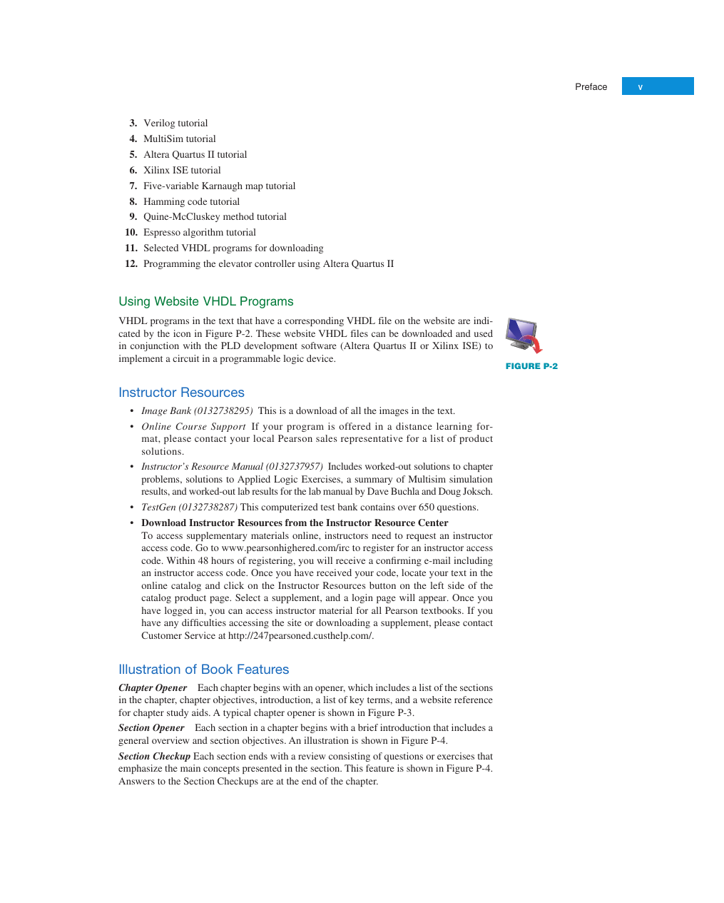
Preface v 3. Verilog tutorial 4. MultiSim tutorial 5. Altera Quartus II tutorial 6. Xilinx ISE tutorial 7. Five-variable Karnaugh map tutorial 8. Hamming code tutorial 9. Quine-McCluskey method tutorial 10. Espresso algorithm tutorial 11. Selected VHDL programs for downloading 12. Programming the elevator controller using Altera Quartus II Using Website VHDL Programs VHDL programs in the text that have a corresponding VHDL file on the website are indi- cated by the icon in Figure P-2. These website VHDL files can be downloaded and used in conjunction with the PLD development software (Altera Quartus II or Xilinx ISE) to implement a circuit in a programmable logic device. Figure P-2 Instructor Resources • Image Bank (0132738295) This is a download of all the images in the text. • Online Course Support If your program is offered in a distance learning for- mat, please contact your local Pearson sales representative for a list of product solutions. • Instructor’s Resource Manual (0132737957) Includes worked-out solutions to chapter problems, solutions to Applied Logic Exercises, a summary of Multisim simulation results, and worked-out lab results for the lab manual by Dave Buchla and Doug Joksch. • TestGen (0132738287) This computerized test bank contains over 650 questions. • Download Instructor Resources from the Instructor Resource Center To access supplementary materials online, instructors need to request an instructor access code. Go to www.pearsonhighered.com/irc to register for an instructor access code. Within 48 hours of registering, you will receive a confirming e-mail including an instructor access code. Once you have received your code, locate your text in the online catalog and click on the Instructor Resources button on the left side of the catalog product page. Select a supplement, and a login page will appear. Once you have logged in, you can access instructor material for all Pearson textbooks. If you have any difficulties accessing the site or downloading a supplement, please contact Customer Service at http://247pearsoned.custhelp.com/. Illustration of Book Features Chapter Opener Each chapter begins with an opener, which includes a list of the sections in the chapter, chapter objectives, introduction, a list of key terms, and a website reference for chapter study aids. A typical chapter opener is shown in Figure P-3. Section Opener Each section in a chapter begins with a brief introduction that includes a general overview and section objectives. An illustration is shown in Figure P-4. Section Checkup Each section ends with a review consisting of questions or exercises that emphasize the main concepts presented in the section. This feature is shown in Figure P-4. Answers to the Section Checkups are at the end of the chapter.
vi Preface M03_FLOY7968_11_SE_C03.indd Page 111 21/04/14 11:18 AM f-445 /204/PH01677/9780132737968_FLOYD/FLOYD_DIGITAL_FUNDAMENTALS11_SE_9780132737968/SE ... Chapter 3 Logic Gates Chapter Outline 3–1 3–2 3–3 3–4 3–5 3–6 3–7 3–8 3–9 The Inverter The AND Gate The OR Gate The NAND Gate The NOR Gate The Exclusive-OR and Exclusive-NOR Gates Programmable Logic Fixed-Function Logic Gates Troubleshooting Chapter Obje Ctives ■ Describe the operation of the inverter, the AND gate, and the OR gate ■ Describe the operation of the NAND gate and the NOR gate ■ Express the operation of NOT, AND, OR, NAND, and NOR gates with Boolean algebra ■ Describe the operation of the exclusive-OR and exclusive-NOR gates ■ Use logic gates in simple applications ■ Recognize and use both the distinctive shape logic gate symbols and the rectangular outline logic gate symbols of ANSI/IEEE Standard 91-1984/Std. 91a-1991 ■ Construct timing diagrams showing the proper time relationships of inputs and outputs for the various logic gates ■ Discuss the basic concepts of programmable logic ■ Make basic comparisons between the major IC technologies—CMOS and bipolar (TTL) ■ Explain how the different series within the CMOS and bipolar (TTL) families differ from each other ■ Define propagation delay time, power dissipation, speed-power product, and fan-out in relation to logic gates ■ List specific fixed-function integrated circuit devices that contain the various logic gates ■ Troubleshoot logic gates for opens and shorts by using the oscilloscope Key t erms Key terms are in order of appearance in the chapter. ■ Inverter ■ Truth table ■ Boolean algebra ■ Complement ■ AND gate ■ OR gate ■ NAND gate ■ NOR gate ■ Exclusive-OR gate ■ Exclusive-NOR gate ■ AND array ■ Fuse ■ Antifuse v isit the Website ■ EPROM ■ EEPROM ■ Flash ■ SRAM ■ Target device ■ JTAG ■ VHDL ■ CMOS ■ Bipolar ■ Propagation delay time ■ Fan-out ■ Unit load Study aids for this chapter are available at http://www.pearsonhighered.com/careersresources/ intr Odu Cti On The emphasis in this chapter is on the operation, application, and troubleshooting of logic gates. The relationship of input and output waveforms of a gate using timing diagrams is thoroughly covered. Logic symbols used to represent the logic gates are in accordance with ANSI/IEEE Standard 91-1984/ Std. 91a-1991. This standard has been adopted by private industry and the military for use in internal documentation as well as published literature. 111 Figure P-3 M05_FLOY7968_11_SE_C05.indd Page 253 02/05/14 1:42 PM f-445 /204/PH01677/9780132737968_FLOYD/FLOYD_DIGITAL_FUNDAMENTALS11_SE_9780132737968/SE ... Implementing Combinational Logic 253 SEcTIon 5–1 CheCKup Answers are at the end of the chapter. 1. Determine the output (1 or 0) of a 4-variable AND-OR-Invert circuit for each of the following input conditions: (a) A = 1, B = 0, C = 1, D = 0 (c) A = 0, B = 1, C = 1, D = 1 (b) A = 1, B = 1, C = 0, D = 1 2. Determine the output (1 or 0) of an exclusive-OR gate for each of the following input conditions: (a) A = 1, B = 0 (c) A = 0, B = 1 (b) A = 1, B = 1 (d) A = 0, B = 0 3. Develop the truth table for a certain 3-input logic circuit with the output expression X = ABC + ABC + A B C + ABC + ABC. 4. Draw the logic diagram for an exclusive-NOR circuit. 5–2 Implementing Combinational Logic In this section, examples are used to illustrate how to implement a logic circuit from a Boolean expression or a truth table. Minimization of a logic circuit using the methods cov- ered in Chapter 4 is also included. After completing this section, you should be able to u Implement a logic circuit from a Boolean expression u Implement a logic circuit from a truth table u Minimize a logic circuit From a Boolean Expression to a Logic Circuit Let’s examine the following Boolean expression: X = AB + CDE A brief inspection shows that this expression is composed of two terms, AB and CDE, with a domain of five variables. The first term is formed by ANDing A with B, and the second term is formed by ANDing C, D, and E. The two terms are then ORed to form the output X. These operations are indicated in the structure of the expression as follows: X = AB + CDE AND OR Note that in this particular expression, the AND operations forming the two individual terms, AB and CDE, must be performed before the terms can be ORed. To implement this Boolean expression, a 2-input AND gate is required to form the term AB, and a 3-input AND gate is needed to form the term CDE. A 2-input OR gate is then required to combine the two AND terms. The resulting logic circuit is shown in Figure 5–9. As another example, let’s implement the following expression: X = AB(CD + EF) Figure P-4 For every Boolean expression there is a logic circuit, and for every logic circuit there is a Boolean expression. infonote Many control programs require logic operations to be performed by a computer. A driver program is a control program that is used with computer peripherals. For example, a mouse driver requires logic tests to determine if a button has been pressed and further logic operations to determine if it has moved, either horizontally or vertically. Within the heart of a microprocessor is the arithmetic logic unit (ALU), which performs these logic operations as directed by program instructions. All of the logic described in this chapter can also be performed by the ALU, given the proper instructions.
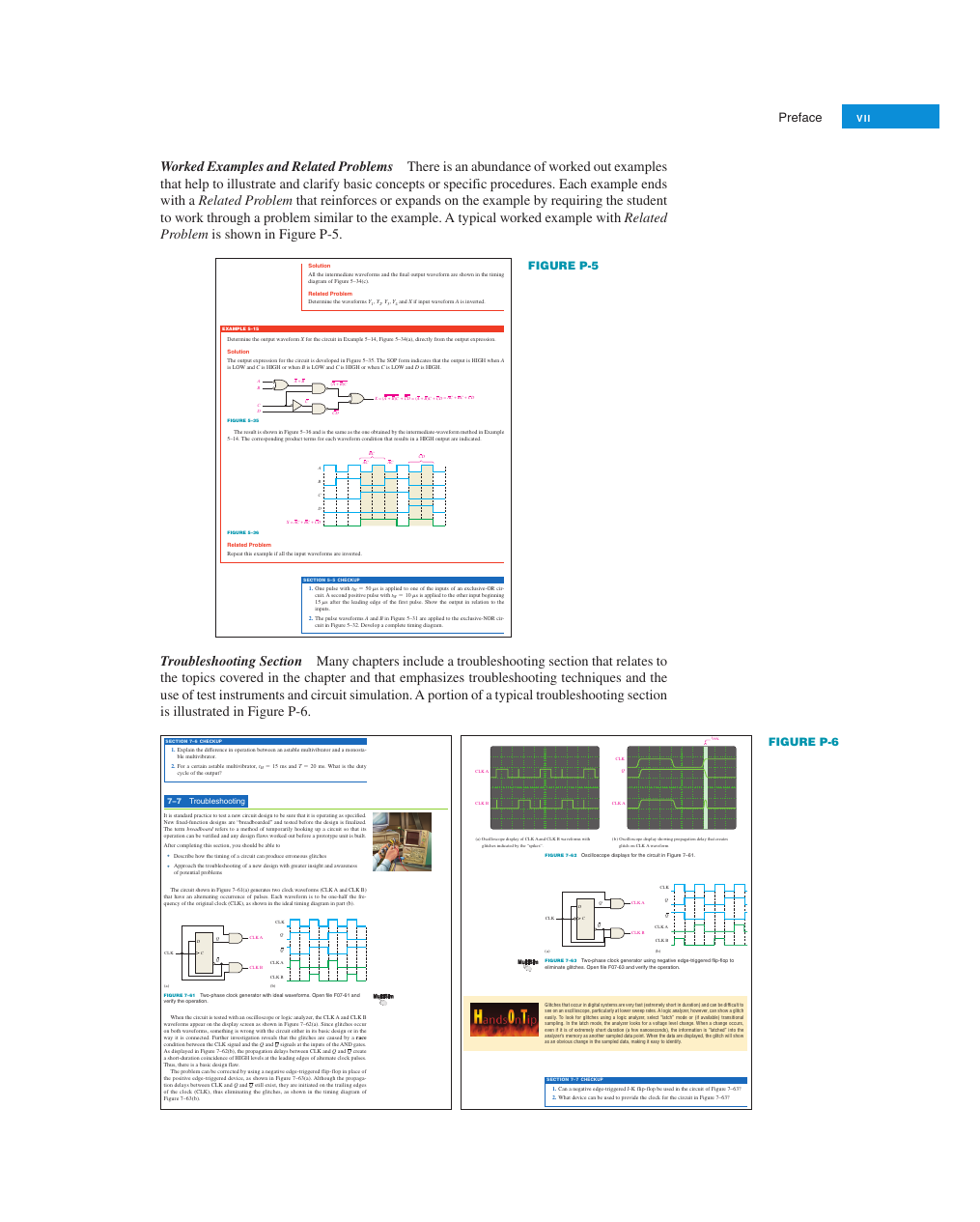
Preface vii Worked Examples and Related Problems There is an abundance of worked out examples that help to illustrate and clarify basic concepts or specific procedures. Each example ends with a Related Problem that reinforces or expands on the example by requiring the student to work through a problem similar to the example. A typical worked example with Related Problem is shown in Figure P-5. /204/PH01677/9780132737968_FLOYD/FLOYD_DIGITAL_FUNDAMENTALS11_SE_9780132737968/SE ... M05_FLOY7968_11_SE_C05.indd Page 268 02/05/14 1:42 PM f-445 268 Combinational Logic Analysis solution All the intermediate waveforms and the final output waveform are shown in the timing diagram of Figure 5–34(c). r elated problem Determine the waveforms Y1, Y2, Y3, Y4 and X if input waveform A is inverted. Figure P-5 EXaMPlE 5–15 Determine the output waveform X for the circuit in Example 5–14, Figure 5–34(a), directly from the output expression. solution The output expression for the circuit is developed in Figure 5–35. The SOP form indicates that the output is HIGH when A is LOW and C is HIGH or when B is LOW and C is HIGH or when C is LOW and D is HIGH. A B C D FIGURE 5–35 A + B C (A + B)C CD X = (A + B)C + CD = (A + B)C + CD = AC + BC + CD The result is shown in Figure 5–36 and is the same as the one obtained by the intermediate-waveform method in Example fg05_03500 5–14. The corresponding product terms for each waveform condition that results in a HIGH output are indicated. BC AC AC CD A B C D X = AC + BC + CD FIGURE 5–36 r elated problem Repeat this example if all the input waveforms are inverted. fg05_03600 SEcTIon 5–5 CheCKup 1. One pulse with tW = 50 ms is applied to one of the inputs of an exclusive-OR cir- cuit. A second positive pulse with tW = 10 ms is applied to the other input beginning 15 ms after the leading edge of the first pulse. Show the output in relation to the inputs. 2. The pulse waveforms A and B in Figure 5–31 are applied to the exclusive-NOR cir- cuit in Figure 5–32. Develop a complete timing diagram. M07_FLOY7968_11_SE_C07.indd Page 413 07/05/14 12:26 PM f-445 /204/PH01677/9780132737968_FLOYD/FLOYD_DIGITAL_FUNDAMENTALS11_SE_9780132737968/SE ... Troubleshooting Section Many chapters include a troubleshooting section that relates to the topics covered in the chapter and that emphasizes troubleshooting techniques and the use of test instruments and circuit simulation. A portion of a typical troubleshooting section is illustrated in Figure P-6. /204/PH01677/9780132737968_FLOYD/FLOYD_DIGITAL_FUNDAMENTALS11_SE_9780132737968/SE ... M07_FLOY7968_11_SE_C07.indd Page 414 12/05/14 7:54 AM f-445 414 Latches, Flip-Flops, and Timers Troubleshooting 413 SEcTIon 7–6 CheCKup 1. Explain the difference in operation between an astable multivibrator and a monosta- ble multivibrator. 2. For a certain astable multivibrator, tH = 15 ms and T = 20 ms. What is the duty cycle of the output? 7–7 Troubleshooting It is standard practice to test a new circuit design to be sure that it is operating as specified. New fixed-function designs are “breadboarded” and tested before the design is finalized. The term breadboard refers to a method of temporarily hooking up a circuit so that its operation can be verified and any design flaws worked out before a prototype unit is built. After completing this section, you should be able to u Describe how the timing of a circuit can produce erroneous glitches u Approach the troubleshooting of a new design with greater insight and awareness of potential problems The circuit shown in Figure 7–61(a) generates two clock waveforms (CLK A and CLK B) that have an alternating occurrence of pulses. Each waveform is to be one-half the fre- quency of the original clock (CLK), as shown in the ideal timing diagram in part (b). D C Q Q CLK (a) CLK A CLK B CLK Q Q CLK A CLK B (b) FIGURE 7–61 Two-phase clock generator with ideal waveforms. Open file F07-61 and verify the operation. When the circuit is tested with an oscilloscope or logic analyzer, the CLK A and CLK B waveforms appear on the display screen as shown in Figure 7–62(a). Since glitches occur on both waveforms, something is wrong with the circuit either in its basic design or in the way it is connected. Further investigation reveals that the glitches are caused by a race condition between the CLK signal and the Q and Q signals at the inputs of the AND gates. As displayed in Figure 7–62(b), the propagation delays between CLK and Q and Q create a short-duration coincidence of HIGH levels at the leading edges of alternate clock pulses. Thus, there is a basic design flaw. The problem can be corrected by using a negative edge-triggered flip-flop in place of the positive edge-triggered device, as shown in Figure 7–63(a). Although the propaga- tion delays between CLK and Q and Q still exist, they are initiated on the trailing edges of the clock (CLK), thus eliminating the glitches, as shown in the timing diagram of Figure 7–63(b). tPHL Figure P-6 CLK A CLK B CLK Q CLK A (a) Oscilloscope display of CLK A and CLK B waveforms with (b) Oscilloscope display showing propagation delay that creates glitches indicated by the “spikes”. glitch on CLK A waveform FIGURE 7–62 Oscilloscope displays for the circuit in Figure 7–61. fg07_06300 D C Q Q CLK (a) CLK A CLK B CLK Q Q CLK A CLK B (b) FIGURE 7–63 Two-phase clock generator using negative edge-triggered flip-flop to eliminate glitches. Open file F07-63 and verify the operation. Glitches that occur in digital systems are very fast (extremely short in duration) and can be difficult to see on an oscilloscope, particularly at lower sweep rates. A logic analyzer, however, can show a glitch easily. To look for glitches using a logic analyzer, select “latch” mode or (if available) transitional sampling. In the latch mode, the analyzer looks for a voltage level change. When a change occurs, even if it is of extremely short duration (a few nanoseconds), the information is “latched” into the analyzer’s memory as another sampled data point. When the data are displayed, the glitch will show as an obvious change in the sampled data, making it easy to identify. SEctIon 7–7 CheCkup 1. Can a negative edge-triggered J-K flip-flop be used in the circuit of Figure 7–63? 2. What device can be used to provide the clock for the circuit in Figure 7–63?
分享到:
收藏