Sheet
1 of 6
Balun Design
In the design of mixers, push-pull amplifiers, baluns are used to link a symmetrical (balanced)
circuit to a asymmetrical (unbalanced) circuit.
Baluns are designed to have a precise 180-degree phase shift, with minimum loss and equal
balanced impedances. In power amplifiers loss of symmetry will degrade efficiency and the
symmetrical port must be well isolated from ground to eliminate parasitic oscillations.
The basic construction/design of a balun consists of two 90-degree phasing lines that provide
the required 180-degree split, and this involves the use of λ/4 and λ/2.
A wire-wound transformer provides an excellent balun. Miniature wirewound transformers are
commercially available covering frequencies from low kHz to beyond 2GHz. They are often
realised with a centre-tapped secondary winding, if grounded this provides a short circuit to
even-mode (common-mode) signals whilst having no effect on the differential (odd-mode)
signal.
Wire-wound transformers are more expensive than the printed or lumped element baluns
described below, which find greater adoption in practical mixer designs. It should be noted
that most of these lumped element and printed baluns do not provide the centre-tapped
ground to even mode signals and this fact must be accounted for in the mixer design.
(1) L-C Balun
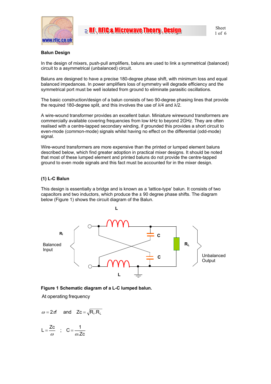
This design is essentially a bridge and is known as a ‘lattice-type’ balun. It consists of two
capacitors and two inductors, which produce the ± 90 degree phase shifts. The diagram
below (Figure 1) shows the circuit diagram of the Balun.
RI
Balanced
Input
L
L
Figure 1 Schematic diagram of a L-C lumped balun.
At
frequency
operating
C
C
RL
Unbalanced
Output
f2
πω
=
and
.RR
Zc
=
L
I
1 C
;
.Zc
ω
=
Zc L
=
ω
�
Sheet
2 of 6
When designing this circuit make sure that the operating frequency is well below the self-
resonant frequencies of the components and take account of pad capacitances.
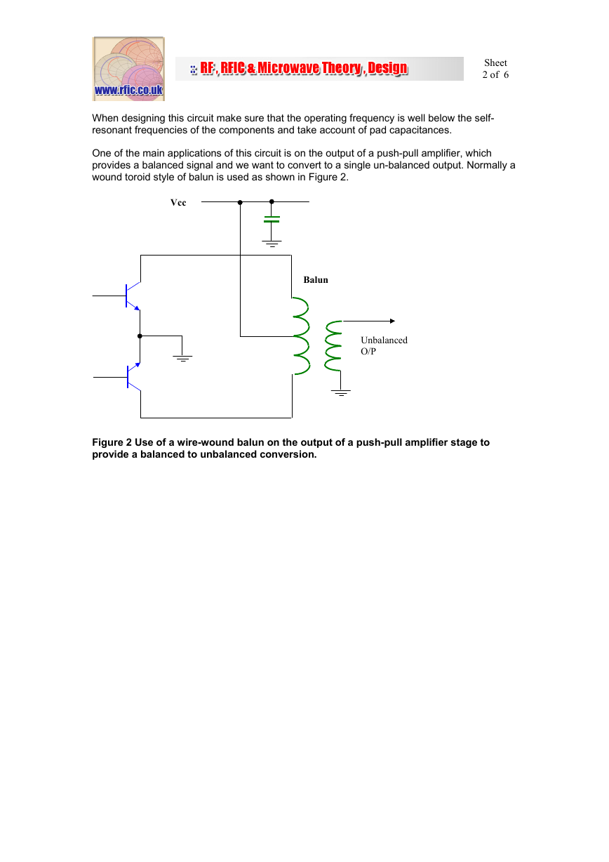
One of the main applications of this circuit is on the output of a push-pull amplifier, which
provides a balanced signal and we want to convert to a single un-balanced output. Normally a
wound toroid style of balun is used as shown in Figure 2.
Vcc
Balun
Unbalanced
O/P
Figure 2 Use of a wire-wound balun on the output of a push-pull amplifier stage to
provide a balanced to unbalanced conversion.
�
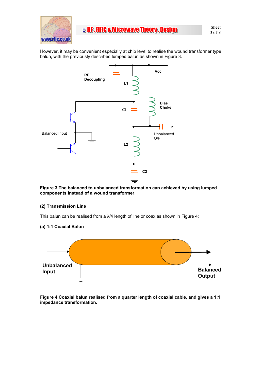
However, it may be convenient especially at chip level to realise the wound transformer type
balun, with the previously described lumped balun as shown in Figure 3.
Sheet
3 of 6
RF
Decoupling
Balanced Input
Vcc
Bias
Choke
Unbalanced
O/P
L1
C1
L2
C2
Figure 3 The balanced to unbalanced transformation can achieved by using lumped
components instead of a wound transformer.
(2) Transmission Line
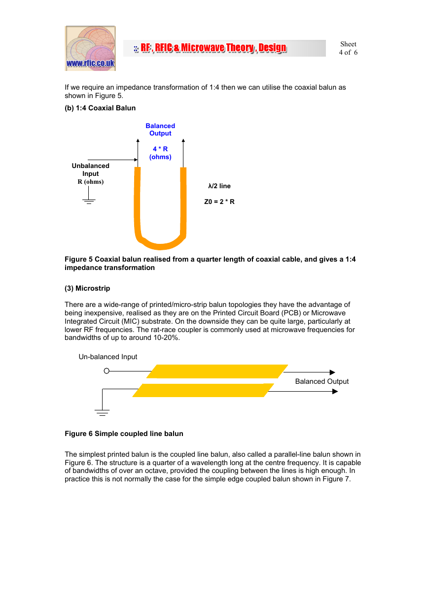
This balun can be realised from a λ/4 length of line or coax as shown in Figure 4:
(a) 1:1 Coaxial Balun
Unbalanced
Input
Balanced
Output
Figure 4 Coaxial balun realised from a quarter length of coaxial cable, and gives a 1:1
impedance transformation.
�
Sheet
4 of 6
If we require an impedance transformation of 1:4 then we can utilise the coaxial balun as
shown in Figure 5.
(b) 1:4 Coaxial Balun
Balanced
Output
4 * R
(ohms)
Unbalanced
Input
R (ohms)
λ/2 line
Z0 = 2 * R
Figure 5 Coaxial balun realised from a quarter length of coaxial cable, and gives a 1:4
impedance transformation
(3) Microstrip
There are a wide-range of printed/micro-strip balun topologies they have the advantage of
being inexpensive, realised as they are on the Printed Circuit Board (PCB) or Microwave
Integrated Circuit (MIC) substrate. On the downside they can be quite large, particularly at
lower RF frequencies. The rat-race coupler is commonly used at microwave frequencies for
bandwidths of up to around 10-20%.
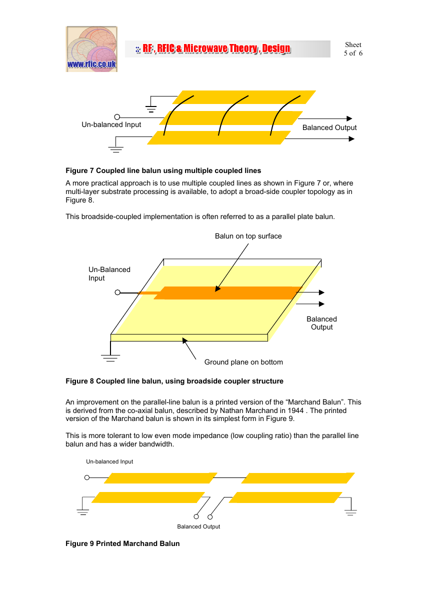
Un-balanced Input
Balanced Output
Figure 6 Simple coupled line balun
The simplest printed balun is the coupled line balun, also called a parallel-line balun shown in
Figure 6. The structure is a quarter of a wavelength long at the centre frequency. It is capable
of bandwidths of over an octave, provided the coupling between the lines is high enough. In
practice this is not normally the case for the simple edge coupled balun shown in Figure 7.
�
Un-balanced Input
Sheet
5 of 6
Balanced Output
Figure 7 Coupled line balun using multiple coupled lines
A more practical approach is to use multiple coupled lines as shown in Figure 7 or, where
multi-layer substrate processing is available, to adopt a broad-side coupler topology as in
Figure 8.
This broadside-coupled implementation is often referred to as a parallel plate balun.
Balun on top surface
Un-Balanced
Input
Balanced
Output
Ground plane on bottom
Figure 8 Coupled line balun, using broadside coupler structure
An improvement on the parallel-line balun is a printed version of the “Marchand Balun”. This
is derived from the co-axial balun, described by Nathan Marchand in 1944 . The printed
version of the Marchand balun is shown in its simplest form in Figure 9.
This is more tolerant to low even mode impedance (low coupling ratio) than the parallel line
balun and has a wider bandwidth.
Un-balanced Input
Balanced Output
Figure 9 Printed Marchand Balun
�
Sheet
6 of 6
As with the parallel line balun, improved performance is obtained if multiple planar section are
used or if a broadside coupling topology is adopted. One draw back to using these printed
baluns at lower RF frequencies is their size. As with the parallel line and Marchand baluns,
the use of broadside, rather than edge, coupling will yield tighter coupling and improved
performance.
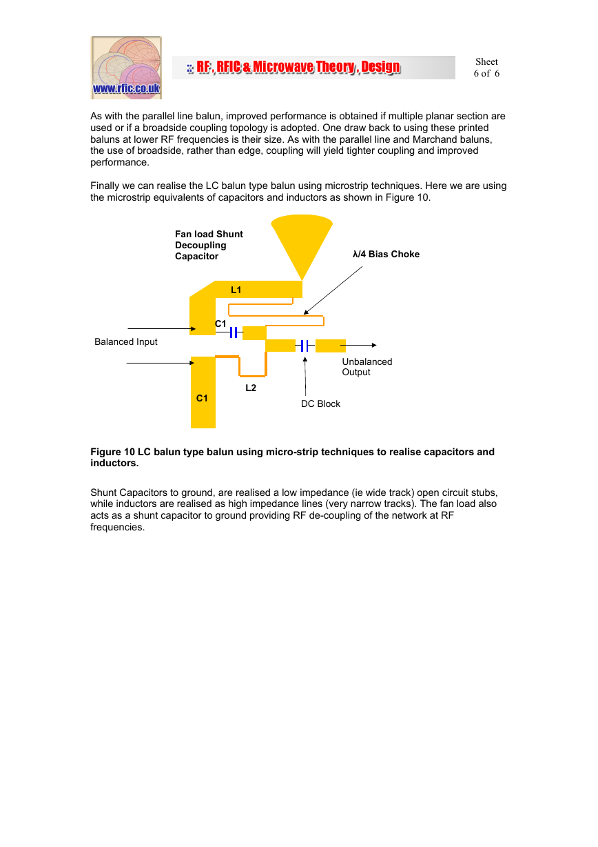
Finally we can realise the LC balun type balun using microstrip techniques. Here we are using
the microstrip equivalents of capacitors and inductors as shown in Figure 10.
Fan load Shunt
Decoupling
Capacitor
L1
C1
Balanced Input
λ/4 Bias Choke
Unbalanced
Output
L2
C1
DC Block
Figure 10 LC balun type balun using micro-strip techniques to realise capacitors and
inductors.
Shunt Capacitors to ground, are realised a low impedance (ie wide track) open circuit stubs,
while inductors are realised as high impedance lines (very narrow tracks). The fan load also
acts as a shunt capacitor to ground providing RF de-coupling of the network at RF
frequencies.
�


 2023年江西萍乡中考道德与法治真题及答案.doc
 2012年重庆南川中考生物真题及答案.doc
 2013年江西师范大学地理学综合及文艺理论基础考研真题.doc
 2020年四川甘孜小升初语文真题及答案I卷.doc
 2020年注册岩土工程师专业基础考试真题及答案.doc
 2023-2024学年福建省厦门市九年级上学期数学月考试题及答案.doc
 2021-2022学年辽宁省沈阳市大东区九年级上学期语文期末试题及答案.doc
 2022-2023学年北京东城区初三第一学期物理期末试卷及答案.doc
 2018上半年江西教师资格初中地理学科知识与教学能力真题及答案.doc
 2012年河北国家公务员申论考试真题及答案-省级.doc
 2020-2021学年江苏省扬州市江都区邵樊片九年级上学期数学第一次质量检测试题及答案.doc
 2022下半年黑龙江教师资格证中学综合素质真题及答案.doc