RK3288 TRM
Chapter 1 Introduction
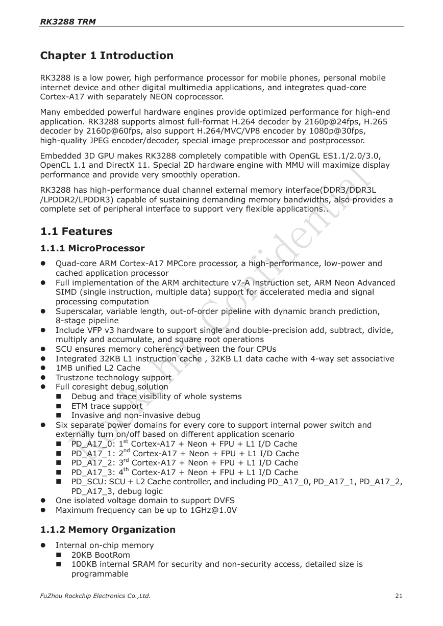
RK3288 is a low power, high performance processor for mobile phones, personal mobile
internet device and other digital multimedia applications, and integrates quad-core
Cortex-A17 with separately NEON coprocessor.
Many embedded powerful hardware engines provide optimized performance for high-end
application. RK3288 supports almost full-format H.264 decoder by 2160p@24fps, H.265
decoder by 2160p@60fps, also support H.264/MVC/VP8 encoder by 1080p@30fps,
high-quality JPEG encoder/decoder, special image preprocessor and postprocessor.
Embedded 3D GPU makes RK3288 completely compatible with OpenGL ES1.1/2.0/3.0,
OpenCL 1.1 and DirectX 11. Special 2D hardware engine with MMU will maximize display
performance and provide very smoothly operation.
RK3288 has high-performance dual channel external memory interface(DDR3/DDR3L
/LPDDR2/LPDDR3) capable of sustaining demanding memory bandwidths, also provides a
complete set of peripheral interface to support very flexible applications..
1.1 Features
1.1.1 MicroProcessor
l Quad-core ARM Cortex-A17 MPCore processor, a high-performance, low-power and
cached application processor
l Full implementation of the ARM architecture v7-A instruction set, ARM Neon Advanced
SIMD (single instruction, multiple data) support for accelerated media and signal
processing computation
l Superscalar, variable length, out-of-order pipeline with dynamic branch prediction,
8-stage pipeline
l Include VFP v3 hardware to support single and double-precision add, subtract, divide,
multiply and accumulate, and square root operations
l SCU ensures memory coherency between the four CPUs
l Integrated 32KB L1 instruction cache , 32KB L1 data cache with 4-way set associative
l 1MB unified L2 Cache
l Trustzone technology support
l Full coresight debug solution
n Debug and trace visibility of whole systems
n ETM trace support
n Invasive and non-invasive debug
l Six separate power domains for every core to support internal power switch and
externally turn on/off based on different application scenario
n PD_A17_0: 1st Cortex-A17 + Neon + FPU + L1 I/D Cache
n PD_A17_1: 2nd Cortex-A17 + Neon + FPU + L1 I/D Cache
n PD_A17_2: 3rd Cortex-A17 + Neon + FPU + L1 I/D Cache
n PD_A17_3: 4th Cortex-A17 + Neon + FPU + L1 I/D Cache
n PD_SCU: SCU + L2 Cache controller, and including PD_A17_0, PD_A17_1, PD_A17_2,
PD_A17_3, debug logic
l One isolated voltage domain to support DVFS
l Maximum frequency can be up to 1GHz@1.0V
1.1.2 Memory Organization
l Internal on-chip memory
n 20KB BootRom
n 100KB internal SRAM for security and non-security access, detailed size is
programmable
FuZhou Rockchip Electronics Co.,Ltd.
21
�
RK3288 TRM
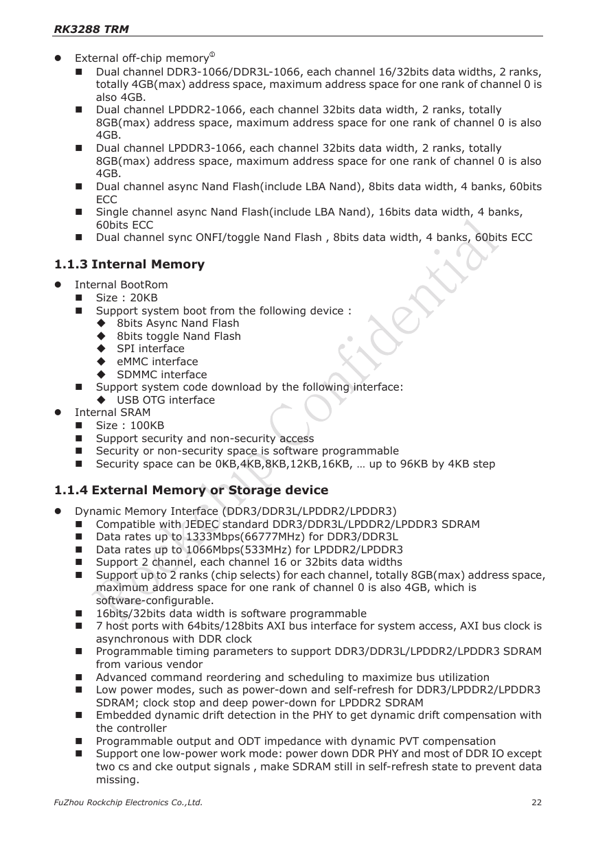
l External off-chip memory
n Dual channel DDR3-1066/DDR3L-1066, each channel 16/32bits data widths, 2 ranks,
totally 4GB(max) address space, maximum address space for one rank of channel 0 is
also 4GB.
n Dual channel LPDDR2-1066, each channel 32bits data width, 2 ranks, totally
8GB(max) address space, maximum address space for one rank of channel 0 is also
4GB.
n Dual channel LPDDR3-1066, each channel 32bits data width, 2 ranks, totally
8GB(max) address space, maximum address space for one rank of channel 0 is also
4GB.
n Dual channel async Nand Flash(include LBA Nand), 8bits data width, 4 banks, 60bits
ECC
n Single channel async Nand Flash(include LBA Nand), 16bits data width, 4 banks,
60bits ECC
n Dual channel sync ONFI/toggle Nand Flash , 8bits data width, 4 banks, 60bits ECC
1.1.3 Internal Memory
l Internal BootRom
n Size : 20KB
n Support system boot from the following device :
u 8bits Async Nand Flash
u 8bits toggle Nand Flash
u SPI interface
u eMMC interface
u SDMMC interface
n Support system code download by the following interface:
u USB OTG interface
l Internal SRAM
n Size : 100KB
n Support security and non-security access
n Security or non-security space is software programmable
n Security space can be 0KB,4KB,8KB,12KB,16KB, … up to 96KB by 4KB step
1.1.4 External Memory or Storage device
l Dynamic Memory Interface (DDR3/DDR3L/LPDDR2/LPDDR3)
n Compatible with JEDEC standard DDR3/DDR3L/LPDDR2/LPDDR3 SDRAM
n Data rates up to 1333Mbps(66777MHz) for DDR3/DDR3L
n Data rates up to 1066Mbps(533MHz) for LPDDR2/LPDDR3
n Support 2 channel, each channel 16 or 32bits data widths
n Support up to 2 ranks (chip selects) for each channel, totally 8GB(max) address space,
maximum address space for one rank of channel 0 is also 4GB, which is
software-configurable.
n 16bits/32bits data width is software programmable
n 7 host ports with 64bits/128bits AXI bus interface for system access, AXI bus clock is
asynchronous with DDR clock
n Programmable timing parameters to support DDR3/DDR3L/LPDDR2/LPDDR3 SDRAM
from various vendor
n Advanced command reordering and scheduling to maximize bus utilization
n Low power modes, such as power-down and self-refresh for DDR3/LPDDR2/LPDDR3
SDRAM; clock stop and deep power-down for LPDDR2 SDRAM
n Embedded dynamic drift detection in the PHY to get dynamic drift compensation with
the controller
n Programmable output and ODT impedance with dynamic PVT compensation
n Support one low-power work mode: power down DDR PHY and most of DDR IO except
two cs and cke output signals , make SDRAM still in self-refresh state to prevent data
missing.
FuZhou Rockchip Electronics Co.,Ltd.
22
�
RK3288 TRM
l Nand Flash Interface
n Support dual channel async nand flash, each channel 8bits, up to 4 banks
n Support dual channel sync DDR nand flash, each channel 8bits, up to 4 banks
n Support LBA nand flash in async or sync mode
n Up to 60bits hardware ECC
n For DDR nand flash, support DLL bypass and 1/4 or 1/8 clock adjust, maximum clock
rate is 75MHz
n For async nand flash, support configurable interface timing , maximum data rate is
16bit/cycle
n Embedded special DMA interface to do data transfer
n Also support data transfer together with general PERI_DMAC in SoC system
l eMMC Interface
n Compatible with standard iNAND interface
n Support MMC4.5 protocol
n Provide eMMC boot sequence to receive boot data from external eMMC device
n Support FIFO over-run and under-run prevention by stopping card clock automatically
n Support CRC generation and error detection
n Embedded clock frequency division control to provide programmable baud rate
n Support block size from 1 to 65535Bytes
n 8bits data bus width
l SD/MMC Interface
n Compatible with SD3.0, MMC ver4.5
n Support FIFO over-run and under-run prevention by stopping card clock automatically
n Support CRC generation and error detection
n Embedded clock frequency division control to provide programmable baud rate
n Support block size from 1 to 65535Bytes
n Data bus width is 4bits
1.1.5 System Component
l CRU (clock & reset unit)
n Support clock gating control for individual components inside RK3288
n One oscillator with 24MHz clock input and 5 embedded PLLs
n Up to 2.2GHz clock output for all PLLs
n Support global soft-reset control for whole SOC, also individual soft-reset for every
components
l PMU(power management unit)
n Multiple configurable work modes to save power by different frequency or automatical
clock gating control or power domain on/off control
n Lots of wakeup sources in different mode
n 4 separate voltage domains
n 12 separate power domains, which can be power up/down by software based on
different application scenes
l Timer
n 8 on-chip 64bits Timers in SoC with interrupt-based operation
n Provide two operation modes: free-running and user-defined count
n Support timer work state checkable
n Fixed 24MHz clock input
l PWM
n Four on-chip PWMs with interrupt-based operation
n Programmable pre-scaled operation to bus clock and then further scaled
n Embedded 32-bit timer/counter facility
FuZhou Rockchip Electronics Co.,Ltd.
23
�
RK3288 TRM
n Support capture mode
n Support continuous mode or one-shot mode
n Provides reference mode and output various duty-cycle waveform
l WatchDog
n 32 bits watchdog counter width
n Counter clock is from apb bus clock
n Counter counts down from a preset value to 0 to indicate the occurrence of a timeout
n WDT can perform two types of operations when timeout occurs:
u Generate a system reset
u First generate an interrupt and if this is not cleared by the service routine by the
time a second timeout occurs then generate a system reset
n Programmable reset pulse length
n Totally 16 defined-ranges of main timeout period
l Bus Architecture
n 128bit/64-bit/32-bit multi-layer AXI/AHB/APB composite bus architecture
n 5 embedded AXI interconnect
u CPU interconnect with four 64-bits AXI masters, one 64-bits AXI slaves, one
32-bits AHB master and lots of 32-bits AHB/APB slaves
u PERI interconnect with two 64-bits AXI masters, one 64-bits AXI slave, five
32-bits AHB masters and lots of 32-bits AHB/APB slaves
u Display interconnect with three 128-bits AXI master, four 64-bits AXI masters and
one 32-bits AHB slave
u GPU interconnect with one 128-bits AXI master with point-to-point AXI-lite
architecture and 32-bits APB slave
u VCODEC interconnect also with two 64-bits AXI master and two 32-bits AHB slave,
they are point-to-point AXI-lite architecture
n For each interconnect with AXI/AHB/APB composite bus, clocks for AXI/AHB/APB
domains are always synchronous, and different integer ratio is supported for them.
n Flexible different QoS solution to improve the utility of bus bandwidth
l Interrupt Controller
n Support 3 PPI interrupt source and 112 SPI interrupt sources input from different
components inside RK3288
n Support 16 softwre-triggered interrupts
n Input interrupt level is fixed , only high-level sensitive
n Two interrupt outputs (nFIQ and nIRQ) separatelyfor each Cortex-A17, both are
low-level sensitive
n Support different interrupt priority for each interrupt source, and they are always
software-programmable
l DMAC
n Micro-code programming based DMA
n The specific instruction set provides flexibility for programming DMA transfers
n Linked list DMA function is supported to complete scatter-gather transfer
n Support internal instruction cache
n Embedded DMA manager thread
n Support data transfer types with memory-to-memory, memory-to-peripheral,
peripheral-to-memory
n Signals the occurrence of various DMA events using the interrupt output signals
n Mapping relationship between each channel and different interrupt outputs is
software-programmable
n Two embedded DMA controller , BUS_DMAC is for bus system, PERI_DMAC is for
peripheral system
n BUS_DMAC features:
u 6 channels totally
FuZhou Rockchip Electronics Co.,Ltd.
24
�
RK3288 TRM
u 6 hardware request from peripherals
u 2 interrupt output
u Dual APB slave interface for register config, designated as secure and non-secure
u Support trustzone technology and programmable secure state for each DMA
channel
n PERI_DMAC features:
u 7 channels totally
u 9 hardware request from peripherals
u 2 interrupt output
u Not support trustzone technology
l Security system
n Support trustzone technology for the following components inside RK3288
u Cortex-A17, support security and non-security mode, switch by software
u BUS_DMAC, support some dedicated channels work only in security mode
u eFuse, only accessed by Cortex-A17 in security mode
u Internal memory , part of space is addressed only in security mode, detailed size
is software-programmable together with TZMA(trustzone memory adapter) and
TZPC(trustzone protection controller)
n Embedded encryption and decryption engine
u Support AES-128/192/256 with ECB, CBC, OFB, CTR, CBC-MAC, CMAC,
XCBC-MAC, XTS and CCM modes
u Supports the DES (ECB and CBC modes) and TDES (EDE and DED) algorithms
u Supports SHA-1, SHA-256 and SHA-512 modes, as well as HMAC
u Support all mathematical operations required to implement the PKA supported
cryptosystems between 128 bits and 3136 bits in size (in steps of 32 bits)
u Support random bits generator from the ring oscillator
u Control the AIB interface to the OTP memory and providing an interface for the
CPU to access to the non-confidential trusted data
u Set the device's security lifecycle state according to the values of various flag
words in the OTP memory
u Provide an firmware interface for secure boot, secure debug
u Provide a security processor sub-system based on an internal 32-bit CPU
n Support security boot
n Support security debug
1.1.6 Video CODEC
l Shared internal memory and bus interface for video decoder and encoder
l Embedded memory management unit(MMU)
l Video Decoder
n Real-time video decoder of MPEG-1, MPEG-2, MPEG-4, H.263, H.264, AVS, VC-1, RV,
VP6/VP8, Sorenson Spark, MVC
n Error detection and concealment support for all video formats
n Output data format is YUV420 semi-planar, and YUV400(monochrome) is also
supported for H.264
: 2160p@24fps (3840x2160)
n H.264 up to HP level 5.2
n MPEG-4 up to ASP level 5 : 1080p@60fps (1920x1088)
n MPEG-2 up to MP
: 2160p@24fps (3840x2160)
: 1080p@60fps (1920x1088)
n MPEG-1 up to MP
: 576p@60fps (720x576)
n H.263
: 1080p@60fps (1920x1088)
n Sorenson Spark
n VC-1 up to AP level 3
: 1080p@30fps (1920x1088)
: 1080p@60fps (1920x1088)
n RV8/RV9/RV10
: 2160p@24fps (3840x2160)
n VP6/VP8
: 1080p@60fps (1920x1088)
n AVS
n MVC
: 2160p@24fps (3840x2160)
FuZhou Rockchip Electronics Co.,Ltd.
25
�
RK3288 TRM
n For AVS, 4:4:4 sampling not supported
n For H.264, image cropping not supported
n For MPEG-4, GMC(global motion compensation) not supported
n For VC-1, upscaling and range mapping are supported in image post-processor
n For MPEG-4 SP/H.263/Sorenson spark, using a modified H.264 in-loop filter to
implement deblocking filter in post-processor unit
l Video Encoder
n Support video encoder for H.264 (BP@level4.0, MP@level4.0, HP@level4.0), MVC and
VP8
n Only support I and P slices, not B slices
n Support error resilience based on constrained intra prediction and slices
n Input data format:
u YCbCr 4:2:0 planar
u YCbCr 4:2:0 semi-planar
u YCbYCr 4:2:2
u CbYCrY 4:2:2 interleaved
u RGB444 and BGR444
u RGB555 and BGR555
u RGB565 and BGR565
u RGB888 and BRG888
u RGB101010 and BRG101010
n Image size is from 96x96 to 1920x1088(Full HD)
n Maximum frame rate is up to 30fps@1920x1080
n Bit rate supported is from 10Kbps to 20Mbps
1.1.7 HEVC Decoder
l Main/Main10 HEVC/H.265 decoderof 4k@60FPS
l Support up to 4096x2304 resolution
l Support up to 100Mbps bit rate
l Embedded memory management unit(MMU)
l Stream error detector (28 IDs)
l Internal 128k cache for bandwidth reduction
l Multi-clock domains and auto clock-gating design for power saving
1.1.8 JPEG CODEC
l JPEG decoder
n Input JPEG file : YCbCr 4:0:0, 4:2:0, 4:2:2, 4:4:0, 4:1:1 and 4:4:4 sampling formats
n Output raw image : YCbCr 4:0:0, 4:2:0, 4:2:2, 4:4:0, 4:1:1 and 4:4:4 semi-planar
n Decoder size is from 48x48 to 8176x8176(66.8Mpixels)
n Support JPEG ROI(region of image) decode
n Maximum data rate is up to 76million pixels per second
n Embedded memory management unit(MMU)
l JPEG encoder
n Input raw image :
u YCbCr 4:2:0 planar
u YCbCr 4:2:0 semi-planar
u YCbYCr 4:2:2
u CbYCrY 4:2:2 interleaved
u RGB444 and BGR444
u RGB555 and BGR555
u RGB565 and BGR565
u RGB888 and BRG888
u RGB101010 and BRG101010
n Output JPEG file : JFIF file format 1.02 or Non-progressive JPEG
FuZhou Rockchip Electronics Co.,Ltd.
26
�
RK3288 TRM
n Encoder image size up to 8192x8192(64million pixels) from 96x32
n Maximum data rate up to 90million pixels per second
n Embedded memory management unit(MMU)
1.1.9 Image Enhancement
l Image pre-processor
n Only used together with HD video encoder inside RK3288, not support stand-alone
mode
n Provides RGB to YCbCr 4:2:0 color space conversion, compatible with BT601, BT709
or user defined coefficients
n Provides YCbCr4:2:2 to YCbCr4:2:0 color space conversion
n Support cropping operation from 8192x8192 to any supported encoding size
n Support rotation with 90 or 270 degrees
l Video stabilization
n Work in combined mode with HD video encoder inside RK3288 and stand-alone mode
n Adaptive motion compensation filter
n Support scene detection from video sequence, encodes key frame when scene change
noticed
l Image Post-Processor (embedded inside video decoder)
n Combined with HD video decoder and JPEG decoder, post-processor can read input
data directly from decoder output to reduce bus bandwidth
n Also work as a stand-alone mode, its input data is from image data stored in external
memory
n Input data format:
u Any format generated by video decoder in combined mode
u YCbCr 4:2:0 semi-planar
u YCbCr 4:2:0 planar
u YCbYCr 4:2:2
u YCrYCb 4:2:2
u CbYCrY 4:2:2
u CrYCbY 4:2:2
n Output data format:
u YCbCr 4:2:0 semi-planar
u YCbYCr 4:2:2
u YCrYCb 4:2:2
u CbYCrY 4:2:2
u CrYCbY 4:2:2
u Fully configurable ARGB channel lengths and locations inside 32bits, such as
ARGB8888, RGB565, ARGB4444 etc.
n Input image size:
u Combined mode: from 48x48 to 8176x8176 (66.8Mpixels)
u Stand-alone mode: width from 48 to 8176,height from 48 to 8176, and maximum
size limited to 16.7Mpixels
u Step size is 16 pixels
n Output image size: from 16x16 to 1920x1088 (horizontal step size 8,vertical step size
2)
n Support image up-scaling:
u Bicubic polynomial interpolation with a four-tap horizontal kernel and a two-tap
vertical kernel
u Arbitrary non-integer scaling ratio separately for both dimensions
u Maximum output width is 3x input width
u Maximum output height is 3x input height
n Support image down-scaling:
u Arbitrary non-integer scaling ratio separately for both dimensions
u Unlimited down-scaling ratio
FuZhou Rockchip Electronics Co.,Ltd.
27
�
RK3288 TRM
n Support YUV to RGB color conversion, compatible with BT.601-5, BT.709 and user
definable conversion coefficient
n Support dithering (2x2 ordered spatial dithering) for 4/5/6bit RGB channel precision
n Support programmable alpha channel and alpha blending operation with the following
overlay input formats:
u 8bit alpha + YUV444, big endian channel order with AYUV8888
u 8bit alpha + 24bit RGB, big endian channel order with ARGB8888
n Support deinterlacing with conditional spatial deinterlace filtering, only compatible
with YUV420 input format
n Support RGB image contrast/brightness/color saturation adjustment
n Support image cropping & digital zoom only for JPEG or stand-alone mode
n Support picture in picture
n Support image rotation (horizontal flip, vertical flip, rotation 90,180 or 270 degrees)
l Image Enhancement-Processor (IEP)
n Image format
u Input data: XRGB/RGB565/YUV420/YUV422
u Output data: ARGB/RGB565/YUV420/YUV422
u The format ARGB/XRGB/RGB565/YUV support swap
u Support YUV semi-planar/planar
u Support BT601_l/BT601_f/BT709_l/BT709_f color space conversion
u Support RGB dither up/down conversion
u Support YUV up/down sampling conversion
u Max source image resolution: 8192x8192
u Max scaled image resolution: 4096x4096
n Enhancement
u Gamma adjustment with programmable mapping table
u Hue/Saturation/Brightness/Contrast enhancement
u Color enhancement with programmable coefficient
u Detail enhancement with filter matrix up to 9x9
u Edge enhancement with filter matrix up to 9x9
u Programmable difference table for detail enhancement
u Programmable distance table for detail and edge enhancement
n Noise reduction
u Compression noise reduction with filter matrix up to 9x9
u Programmable difference table for compression noise reduction
u Programmable distance table for compression noise reduction
u Spatial sampling noise reduction
u Temporal sampling noise reduction
u Optional coefficient for sampling noise reduction
n Scaling
u Horizontal down-scaling with vertical down-scaling
u Horizontal down-scaling with vertical up-scaling
u Horizontal up-scaling with vertical down-scaling
u Horizontal up-scaling with vertical up-scaling
u Arbitrary non-integer scaling ratio, from 1/16 to 16
n Deinterlace
u Input 4 fields, output 2 frames mode
u Input 4 fields, output 1 frames mode
u Input 2 fields, output 1 frames mode
u Programmable motion detection coefficient
u Programmable high frequency factor
u Programmable edge interpolation parameter
u Source width up to 1920
n Interface
u Programmable direct path to VOP
FuZhou Rockchip Electronics Co.,Ltd.
28
�



 2023年江西萍乡中考道德与法治真题及答案.doc
 2012年重庆南川中考生物真题及答案.doc
 2013年江西师范大学地理学综合及文艺理论基础考研真题.doc
 2020年四川甘孜小升初语文真题及答案I卷.doc
 2020年注册岩土工程师专业基础考试真题及答案.doc
 2023-2024学年福建省厦门市九年级上学期数学月考试题及答案.doc
 2021-2022学年辽宁省沈阳市大东区九年级上学期语文期末试题及答案.doc
 2022-2023学年北京东城区初三第一学期物理期末试卷及答案.doc
 2018上半年江西教师资格初中地理学科知识与教学能力真题及答案.doc
 2012年河北国家公务员申论考试真题及答案-省级.doc
 2020-2021学年江苏省扬州市江都区邵樊片九年级上学期数学第一次质量检测试题及答案.doc
 2022下半年黑龙江教师资格证中学综合素质真题及答案.doc