T. Lhommeaua,b,c,*, C. Martina, M. Karamaa , R. Meuret, M. Mermet-Guyennetb
a École National d’Ingenieurs de Tarbes. 47 Avenue d’Azereix BP 1629, 65016 Tarbes, France
b PEARL, Alstom Transport Tarbes. Rue du Docteur Guinier -BP4, 65600 Semeac, France
c Hispano-Suiza. RP René Ravaux site de Villaroche-Réau , 77550 Réau, France
Base-plate solder reliability study of IGBT modules for aeronautical
application
*Tel.: +33 / (0) – 562.53.43.41
*Fax: +33 / (0) – 562.53.44.81
*E-Mail: tony.lhommeau@lab-pearl.com
Acknowledgements
The authors would like to thank Mr Pascal Leclerc and Mr François Le Ray, Hispano-Suiza Company,
and Dr Joël Alexis, ENIT, for the quality of the experimental micro sections done on the IGBT
component, Dr Steve Jones, Technical director of Semelab Company PLC in the UK and Dr Xavier
Perpinyà of PEARL for the technical discussions.
Keywords
“IGBT module”, “Reliability”, “Finite Element Method”, “Aeronautical constraint”, “Acceleration
factor”
Abstract
In this work, a thermal fatigue study on IGBT modules for aeronautical application is carried out,
based on accelerated thermal tests and the thermo-mechanical process simulation. The 3D thermal
simulation gives us the impact of the delamination degree on the IGBT module thermal behavior and
fixes the failure criterion. Element Finite thermo-mechanical simulation based and the metallurgical
fatigue observations permit providing the predictive indication on the accelerated factors to predict the
crack apparition and its propagation inside the solder on the basis of the creep energy dissipated.
Introduction
The more electrical aircraft goals are reducing the weight and the operating cost by the replacement
of hydraulic equipment by electrical system. These systems could be placed in harsh environment as
the engine nacelle. The reliability of these systems is strongly influenced by the power component, the
IGBT module in this case (one of the inverter master pieces). The IGBT module electronic function,
assured by the silicon die, is a power switch drive at low voltage. Under real application the dice
generated heat flux where is conducted across the assembly, the thermal performances of the
packaging are one key that ensures a good reliability of the silicon die.
The IGBT module structure is composed of a multilayer materials braze. Experimentally we have
observed a critical failure mode in accelerated thermal cycles: the solder delamination between the
base plate and the substrate metalized. To estimate the ageing acceleration factor relationship between
accelerated thermal cycles and a now-wear-out module, we determinate a methodology in two steps.
In this work, we have studied the IGBT multilayer structure and their environment to know the
material assembly response to thermal fatigue. Consequently, accelerated thermal cycles have been
done to identify their effects by Scan Acoustic Microscopy (SAM). After that, thermal simulations
have been done to define the thermal behavior of the assembly along the delamination evolution.
Finally, a finite element model has been done to calculate the creep deformation and the creep
energy dissipation on the solder. The study of material fatigue phenomena permits us to explain the
crack formation, as well as its propagation, and retains from the bibliography the mechanical
�
predictive model the accelerate fatigue material coefficient extracted from the Coffin-Manson and
Paris Law for predict the life time of the IGBT lifetime linked to this degradation process.
I. Experimental study
I.1. Sandwich structure of the IGBT module assembly
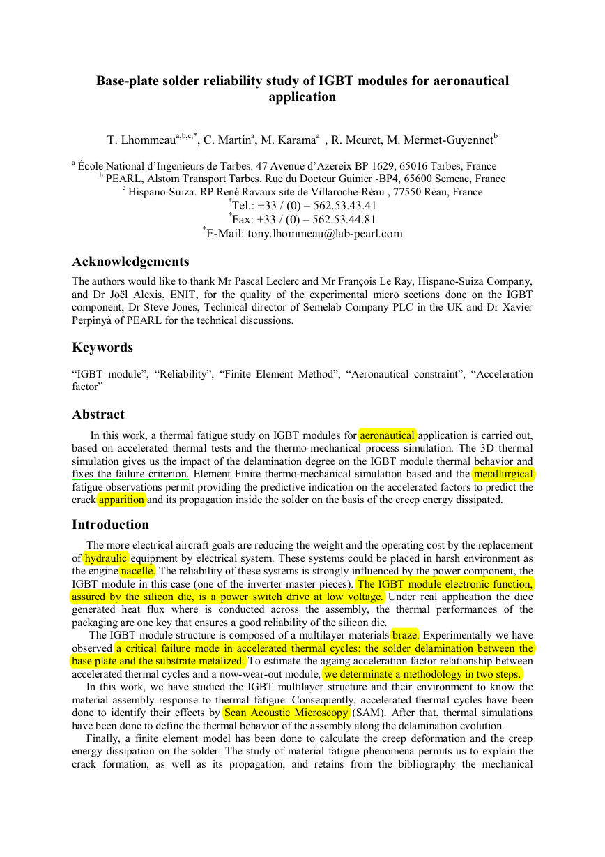
The IGBT module is composed of a multilayer structure encapsulated in a plastic shell, in which
the silicone gel is included: performing the electrical insulation, mechanical and moisture protection
functions. This sandwich structure, see Fig.1, should meet two aims: a high electrical insulation
(600V) by ceramic substrate use to be assembled using screws (base plate) on the support and a low
thermal resistance thanks to the design of slim thickness' and high thermal conductivity of its parts.
The chip is attached on the metalized ceramic substrate by high temperature solder and the ceramic
substrate on the base plate by medium temperature solder.
Chips
Chip solder
Base plate
solder
DAB
Base plate
Fig. 1: Multilayer structure of the IGBT module
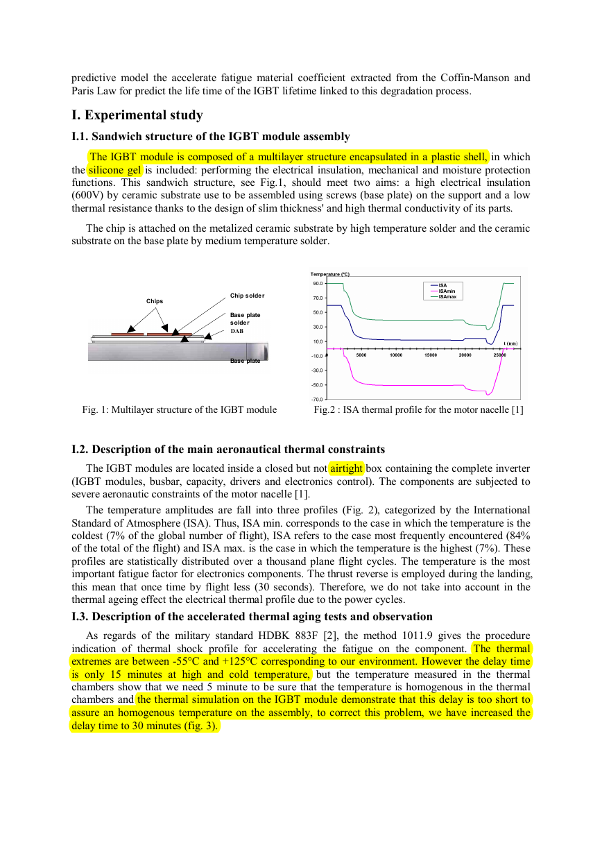
Fig.2 : ISA thermal profile for the motor nacelle [1]
I.2. Description of the main aeronautical thermal constraints
The IGBT modules are located inside a closed but not airtight box containing the complete inverter
(IGBT modules, busbar, capacity, drivers and electronics control). The components are subjected to
severe aeronautic constraints of the motor nacelle [1].
The temperature amplitudes are fall into three profiles (Fig. 2), categorized by the International
Standard of Atmosphere (ISA). Thus, ISA min. corresponds to the case in which the temperature is the
coldest (7% of the global number of flight), ISA refers to the case most frequently encountered (84%
of the total of the flight) and ISA max. is the case in which the temperature is the highest (7%). These
profiles are statistically distributed over a thousand plane flight cycles. The temperature is the most
important fatigue factor for electronics components. The thrust reverse is employed during the landing,
this mean that once time by flight less (30 seconds). Therefore, we do not take into account in the
thermal ageing effect the electrical thermal profile due to the power cycles.
I.3. Description of the accelerated thermal aging tests and observation
As regards of the military standard HDBK 883F [2], the method 1011.9 gives the procedure
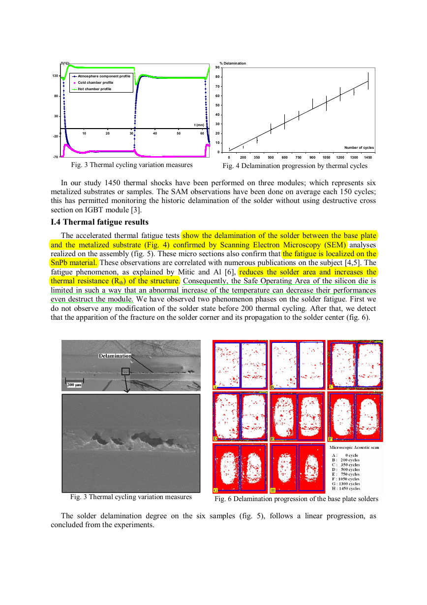
indication of thermal shock profile for accelerating the fatigue on the component. The thermal
extremes are between -55°C and +125°C corresponding to our environment. However the delay time
is only 15 minutes at high and cold temperature, but the temperature measured in the thermal
chambers show that we need 5 minute to be sure that the temperature is homogenous in the thermal
chambers and the thermal simulation on the IGBT module demonstrate that this delay is too short to
assure an homogenous temperature on the assembly, to correct this problem, we have increased the
delay time to 30 minutes (fig. 3).
�
T(°C)
130
80
30
0
-20
-70
Atmosphere component profile
Cold chamber profile
Hot chamber profile
10
20
30
40
50
t (mn)
60
% Delamination
90
80
70
60
50
40
30
20
10
0
Number of cycles
0
200
350
1450
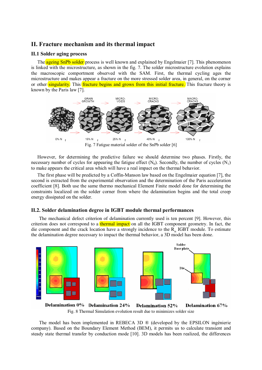
Fig. 4 Delamination progression by thermal cycles
1200
1300
900
1050
500
600
750
Fig. 3 Thermal cycling variation measures
In our study 1450 thermal shocks have been performed on three modules; which represents six
metalized substrates or samples. The SAM observations have been done on average each 150 cycles;
this has permitted monitoring the historic delamination of the solder without using destructive cross
section on IGBT module [3].
I.4 Thermal fatigue results
The accelerated thermal fatigue tests show the delamination of the solder between the base plate
and the metalized substrate (Fig. 4) confirmed by Scanning Electron Microscopy (SEM) analyses
realized on the assembly (fig. 5). These micro sections also confirm that the fatigue is localized on the
SnPb material. These observations are correlated with numerous publications on the subject [4,5]. The
fatigue phenomenon, as explained by Mitic and Al [6], reduces the solder area and increases the
thermal resistance (Rth) of the structure. Consequently, the Safe Operating Area of the silicon die is
limited in such a way that an abnormal increase of the temperature can decrease their performances
even destruct the module. We have observed two phenomenon phases on the solder fatigue. First we
do not observe any modification of the solder state before 200 thermal cycling. After that, we detect
that the apparition of the fracture on the solder corner and its propagation to the solder center (fig. 6).
Fig. 3 Thermal cycling variation measures
The solder delamination degree on the six samples (fig. 5), follows a linear progression, as
Fig. 6 Delamination progression of the base plate solders
concluded from the experiments.
�
II. Fracture mechanism and its thermal impact
II.1 Solder aging process
The ageing SnPb solder process is well known and explained by Engelmaier [7]. This phenomenon
is linked with the microstructure, as shown in the fig. 7. The solder microstructure evolution explains
the macroscopic comportment observed with the SAM. First, the thermal cycling ages the
microstructure and makes appear a fracture on the more stressed solder area, in general, on the corner
or other singularity. This fracture begins and grows from this initial fracture. This fracture theory is
known by the Paris law [7].
Fig. 7 Fatigue material solder of the SnPb solder [6]
However, for determining the predictive failure we should determine two phases. Firstly, the
necessary number of cycles for appearing the fatigue effect (N0). Secondly, the number of cycles (N1)
to make appears the critical area which will have a real impact on the thermal behavior.
The first phase will be predicted by a Coffin-Manson law based on the Engelmaier equation [7], the
second is extracted from the experimental observation and the determination of the Paris acceleration
coefficient [8]. Both use the same thermo mechanical Element Finite model done for determining the
constraints localized on the solder corner from where the delamination begins and the total creep
energy dissipated on the solder.
II.2. Solder delamination degree in IGBT module thermal performances
The mechanical defect criterion of delamination currently used is ten percent [9]. However, this
criterion does not correspond to a thermal impact on all the IGBT component geometry. In fact, the
die component and the crack location have a strongly incidence to the Rth IGBT module. To estimate
the delamination degree necessary to impact the thermal behavior, a 3D model has been done.
Fig. 8 Thermal Simulation evolution result due to minimizes solder size
The model has been implemented in REBECA 3D ® (developed by the EPSILON ingénierie
company). Based on the Boundary Element Method (BEM), it permits us to calculate transient and
steady state thermal transfer by conduction mode [10]. 3D models has been realized, the differences
�
between them is the base plate solder geometry for reproducing the delamination occurring during the
thermal cycles, and accounting the crack and the solder geometry change from the initial state 0%,
24%, 52% and 67 % of delamination (fig. 8).
To be representative of the used experiments conditions, the boundaries conditions take into
account of the natural convection (no forced air or water cooling systems were used), the value taken
here is 5 W/m².K.
Rth % evolution
40
Rth % evolution
35
30
25
20
15
10
5
0
Delamination surface %
71
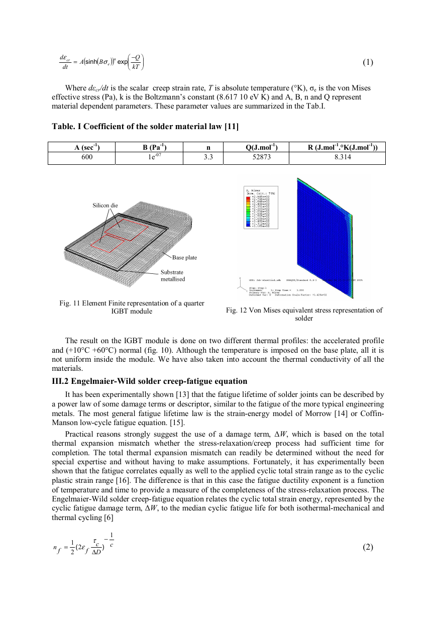
Fig. 10 Thermal cycles profile done on the thermal model
1
11
21
31
41
51
61
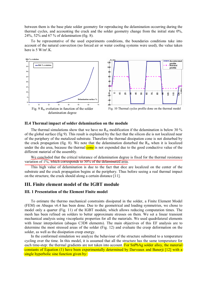
Fig. 9 Rth evolution in function of the solder
delamination degree
II.4 Thermal impact of solder delamination on the module
The thermal simulations show that we have no Rth modification if the delamination is below 30 %
of the global surface (fig 9). This result is explained by the fact that the silicon die is not localized near
of the periphery of the metalized substrate. Therefore the thermal dissipation cone is not disturbed by
the crack propagation (fig. 8). We note that the delamination disturbed the Rth when it is localized
under the die area, because the thermal cone is not expended due to the good conductive value of the
different material of the assembly.
We concluded that the critical tolerance of delamination degree is fixed for the thermal resistance
variation of 1%, which corresponds to 30% of the delaminated area.
This high value of delamination is due to the fact that dice are localized on the center of the
substrate and the crack propagation begins at the periphery. Thus before seeing a real thermal impact
on the structure, the crack should along a certain distance [11].
III. Finite element model of the IGBT module
III. 1 Presentation of the Element Finite model
To estimate the thermo mechanical constraints dissipated in the solder, a Finite Element Model
(FEM) on Abaqus v6.4 has been done. Due to the geometrical and loading symmetries, we chose to
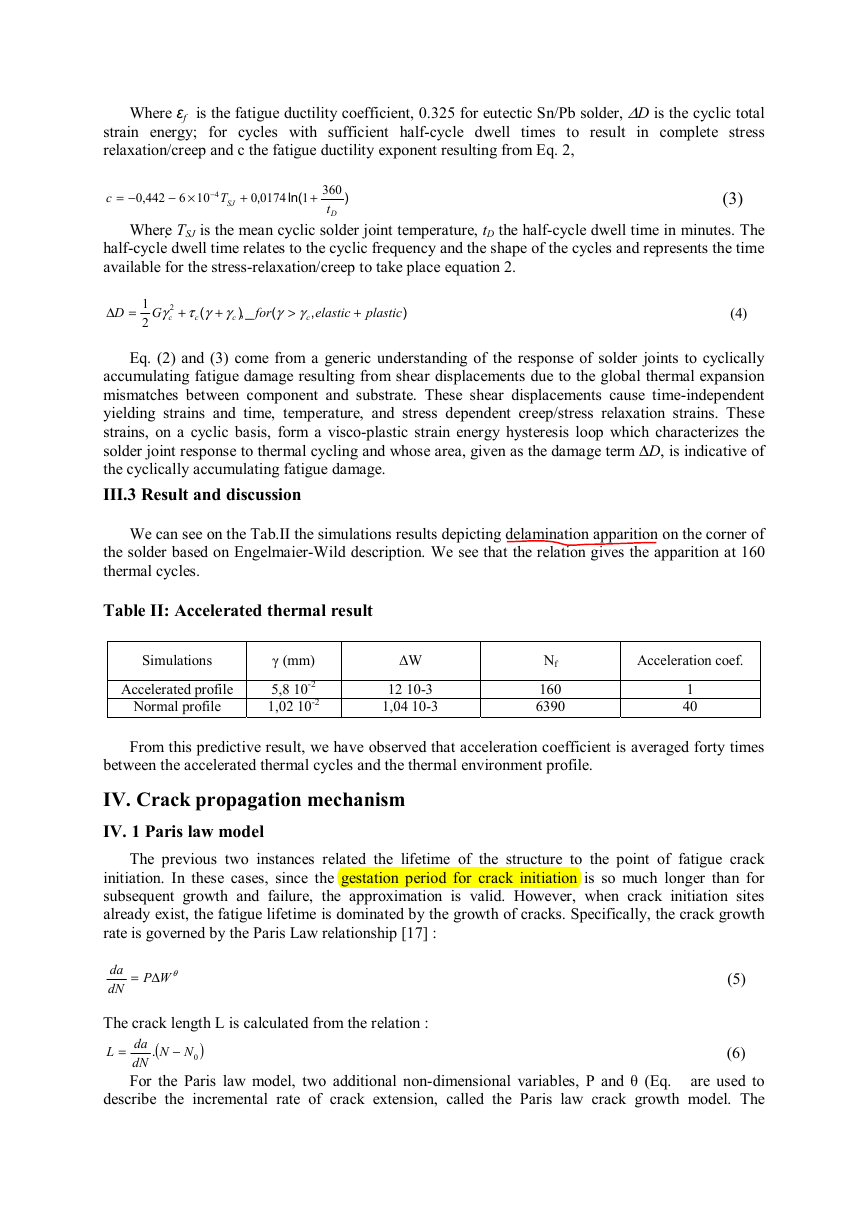
model only a quarter (Fig. 11) of the IGBT module, which allows reducing computation times. The
mesh has been refined on solders to better approximate stresses on them. We set a linear transient
mechanical analysis using viscoplastic properties for all the materials. We used quadrilateral elements
with linear interpolation (abaqus C3D8 elements). The main objectives of this EF analysis are to
determine the most stressed areas of the solder (Fig. 12) and evaluate the creep deformation on the
solder, as well as the dissipation creep energy.
In the conformed simulation we analyze the behaviour of the structure submitted to a temperature
cycling over the time. In this model, it is assumed that all the structure has the same temperature for
each time-step: the thermal gradients are not taken into account. For SnPbAg solder alloy, the material
constants of Equation (1) have been experimentally determined by Darveaux and Banerji [12] with a
single hyperbolic sine function given by:
�
ε
d
cr
dt
=
(
sinh σ
A
e
B
(
)
)
n
−
Q
exp
kT
(1)
Where dεcr/dt is the scalar creep strain rate, T is absolute temperature (°K), σe is the von Mises
effective stress (Pa), k is the Boltzmann’s constant (8.617 10 eV K) and A, B, n and Q represent
material dependent parameters. These parameter values are summarized in the Tab.I.
Table. I Coefficient of the solder material law [11]
A (sec-1)
600
B (Pa-1)
1e-07
n
3.3
Q(J.mol-1)
52873
R (J.mol-1.°K(J.mol-1))
8.314
Fig. 11 Element Finite representation of a quarter
IGBT module
Fig. 12 Von Mises equivalent stress representation of
solder
The result on the IGBT module is done on two different thermal profiles: the accelerated profile
and (+10°C +60°C) normal (fig. 10). Although the temperature is imposed on the base plate, all it is
not uniform inside the module. We have also taken into account the thermal conductivity of all the
materials.
III.2 Engelmaier-Wild solder creep-fatigue equation
It has been experimentally shown [13] that the fatigue lifetime of solder joints can be described by
a power law of some damage terms or descriptor, similar to the fatigue of the more typical engineering
metals. The most general fatigue lifetime law is the strain-energy model of Morrow [14] or Coffin-
Manson low-cycle fatigue equation. [15].
Practical reasons strongly suggest the use of a damage term, ∆W, which is based on the total
thermal expansion mismatch whether the stress-relaxation/creep process had sufficient time for
completion. The total thermal expansion mismatch can readily be determined without the need for
special expertise and without having to make assumptions. Fortunately, it has experimentally been
shown that the fatigue correlates equally as well to the applied cyclic total strain range as to the cyclic
plastic strain range [16]. The difference is that in this case the fatigue ductility exponent is a function
of temperature and time to provide a measure of the completeness of the stress-relaxation process. The
Engelmaier-Wild solder creep-fatigue equation relates the cyclic total strain energy, represented by the
cyclic fatigue damage term, ∆W, to the median cyclic fatigue life for both isothermal-mechanical and
thermal cycling [6]
=
1
2
(
ε
2
f
1
c
−
τ
c
∆
D
)
fn
(2)
�
Where εf is the fatigue ductility coefficient, 0.325 for eutectic Sn/Pb solder, ∆D is the cyclic total
strain energy; for cycles with sufficient half-cycle dwell times to result in complete stress
relaxation/creep and c the fatigue ductility exponent resulting from Eq. 2,
c
,
0174
0
0,442
×−
ln(
1
−=
10
+
+
6
)
−
4
(3)
T
SJ
360
t
D
Where TSJ is the mean cyclic solder joint temperature, tD the half-cycle dwell time in minutes. The
half-cycle dwell time relates to the cyclic frequency and the shape of the cycles and represents the time
available for the stress-relaxation/creep to take place equation 2.
=∆
D
plastic
elastic
γγτγ2
c
c
γγ
(
c
(4)
for
_,)
G
+
>
+
+
)
(
,
c
1
2
Eq. (2) and (3) come from a generic understanding of the response of solder joints to cyclically
accumulating fatigue damage resulting from shear displacements due to the global thermal expansion
mismatches between component and substrate. These shear displacements cause time-independent
yielding strains and time, temperature, and stress dependent creep/stress relaxation strains. These
strains, on a cyclic basis, form a visco-plastic strain energy hysteresis loop which characterizes the
solder joint response to thermal cycling and whose area, given as the damage term ∆D, is indicative of
the cyclically accumulating fatigue damage.
III.3 Result and discussion
We can see on the Tab.II the simulations results depicting delamination apparition on the corner of
the solder based on Engelmaier-Wild description. We see that the relation gives the apparition at 160
thermal cycles.
Table II: Accelerated thermal result
Simulations
Accelerated profile
Normal profile
γ (mm)
5,8 10-2
1,02 10-2
∆W
12 10-3
1,04 10-3
Nf
160
6390
Acceleration coef.
1
40
From this predictive result, we have observed that acceleration coefficient is averaged forty times
between the accelerated thermal cycles and the thermal environment profile.
IV. Crack propagation mechanism
IV. 1 Paris law model
The previous two instances related the lifetime of the structure to the point of fatigue crack
initiation. In these cases, since the gestation period for crack initiation is so much longer than for
subsequent growth and failure, the approximation is valid. However, when crack initiation sites
already exist, the fatigue lifetime is dominated by the growth of cracks. Specifically, the crack growth
rate is governed by the Paris Law relationship [17] :
da
dN
∆=
θWP
(5)
The crack length L is calculated from the relation :
L
)0NN
−
(
.
=
da
dN
For the Paris law model, two additional non-dimensional variables, P and θ (Eq. are used to
describe the incremental rate of crack extension, called the Paris law crack growth model. The
(6)
�
delamination percentage is the ratio between the total surface and the no delaminated one. The crack
propagation speed along the long and small side is the same significant than the mechanical constraint
are similar. The corner of the solder is quickly delaminated due to the high mechanical stress localized
to this region (Fig. 11). The crack length is calculated from the percentage delamination observed (fig.
4) with the relation issue from the geometrical simplification of the solder from fig. 13 :
−
L
=
a
2
L
2
S
Delam
(7)
Where a represents the crack length, L the square side and SDelam the delamination percentage
extract from the experimental data. The thermal simulation gives the limit percentage of IGBT module
limited at 30 % of delamination. This is corresponding from the Fig. 13. The calculated crack
propagation value is fitted with the experimental value, the result is give on the fig. 14.
Fig. 13 Format of the calculus methodology
fig. 14 Crack length propagation
IV.3 Accelerated coefficient and extracted lifetime prediction
We can deduce the acceleration coefficient between the accelerated thermal cycles and the
normal profile equ. 5.
da
Accelerate
d
dN
Normal
dN
da
A
Paris
=
∆=
WP
∆
WP
θ
d
Accelerate
θ
Normal
∆=
W
Accelerate
d
∆
W
Normal
θ
(8)
To deduce the AParis acceleration coefficient, it is necessary to deduce the θ coefficient. To estimate
this coefficient it is necessary to cycle few samples from different thermal cycling [17]. Data can be
founded on the bibliography for the SnPb solder. These results can not be extrapolated, because their
determination is not only depend on the condition and methodology followed but also the value of θ
varies from 0.7376 to 1.36 [18, 19].
Table III Predictive number of cycle of failure by crack grow progression
θ coefficient
0.7376
1.36
AParis
5
24
Predictive number of
cycles
2000
9600
Predictive total
number of cycle N1
8390
15990
Global influence
of N1 (%)
25 %
60 %
This high variation is very different because the creep energy dissipated is global in volume. In
fact, the energy is concentrated on the solder periphery, fact which explains the difference value
�


 2023年江西萍乡中考道德与法治真题及答案.doc
 2012年重庆南川中考生物真题及答案.doc
 2013年江西师范大学地理学综合及文艺理论基础考研真题.doc
 2020年四川甘孜小升初语文真题及答案I卷.doc
 2020年注册岩土工程师专业基础考试真题及答案.doc
 2023-2024学年福建省厦门市九年级上学期数学月考试题及答案.doc
 2021-2022学年辽宁省沈阳市大东区九年级上学期语文期末试题及答案.doc
 2022-2023学年北京东城区初三第一学期物理期末试卷及答案.doc
 2018上半年江西教师资格初中地理学科知识与教学能力真题及答案.doc
 2012年河北国家公务员申论考试真题及答案-省级.doc
 2020-2021学年江苏省扬州市江都区邵樊片九年级上学期数学第一次质量检测试题及答案.doc
 2022下半年黑龙江教师资格证中学综合素质真题及答案.doc