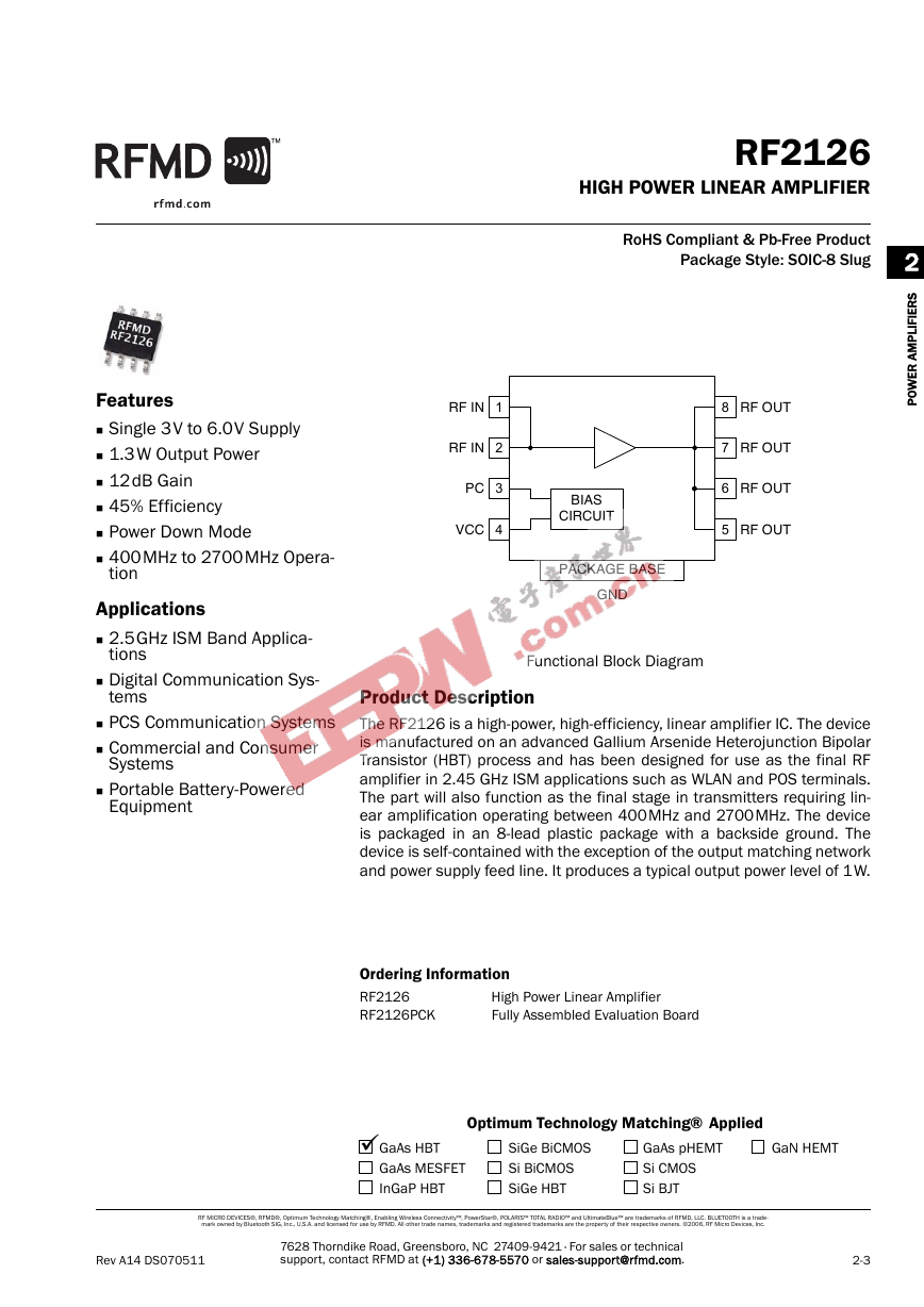
2-32POWER AMPLIFIERSOptimum Technology Matching® AppliedGaAs HBTInGaP HBTGaAs MESFETSiGe BiCMOSSi BiCMOSSiGe HBTGaAs pHEMTSi CMOSSi BJTGaN HEMTFunctional Block DiagramRF MICRO DEVICES®, RFMD®, Optimum Technology Matching®, Enabling Wireless Connectivity™, PowerStar®, POLARIS™ TOTAL RADIO™ and UltimateBlue™ are trademarks of RFMD, LLC. BLUETOOTH is a trade-mark owned by Bluetooth SIG, Inc., U.S.A. and licensed for use by RFMD. All other trade names, trademarks and registered trademarks are the property of their respective owners. ©2006, RF Micro Devices, Inc.Product Description7628 Thorndike Road, Greensboro, NC 27409-9421 · For sales or technical support, contact RFMD at (+1) 336-678-5570 or sales-support@rfmd.com.Ordering Information12348765 RF INRF INPCVCCRF OUTRF OUTRF OUTRF OUTBIASCIRCUITPACKAGE BASEGNDRF2126HIGH POWER LINEAR AMPLIFIERThe RF2126 is a high-power, high-efficiency, linear amplifier IC. The deviceis manufactured on an advanced Gallium Arsenide Heterojunction BipolarTransistor (HBT) process and has been designed for use as the final RFamplifier in 2.45 GHz ISM applications such as WLAN and POS terminals.The part will also function as the final stage in transmitters requiring lin-ear amplification operating between 400MHz and 2700MHz. The deviceis packaged in an 8-lead plastic package with a backside ground. Thedevice is self-contained with the exception of the output matching networkand power supply feed line. It produces a typical output power level of 1W.FeaturesSingle 3V to 6.0V Supply1.3W Output Power12dB Gain45% EfficiencyPower Down Mode400MHz to 2700MHz Opera-tionApplications2.5GHz ISM Band Applica-tionsDigital Communication Sys-temsPCS Communication SystemsCommercial and Consumer SystemsPortable Battery-Powered EquipmentRF2126High Power Linear AmplifierRF2126PCKFully Assembled Evaluation BoardRev A14 DS070511RF2126High Power Linear AmplifierRoHS Compliant & Pb-Free ProductPackage Style: SOIC-8 Slug�
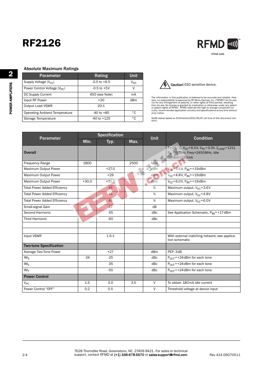
2POWER AMPLIFIERS2-4RF2126Rev A14 DS0705117628 Thorndike Road, Greensboro, NC 27409-9421 · For sales or technical support, contact RFMD at (+1) 336-678-5570 or sales-support@rfmd.com.Absolute Maximum RatingsParameterRatingUnitSupply Voltage (VCC)-0.5 to +6.5VDCPower Control Voltage (VPC)-0.5 to +5VVDC Supply Current450 (see Note)mAInput RF Power+20dBmOutput Load VSWR20:1Operating Ambient Temperature-40 to +85°CStorage Temperature-40 to +125°CParameterSpecificationUnitConditionMin.Typ.Max.OverallT=25°C, VCC=6.0V, VPC=3.0V, ZLOAD=12Ω, Pin = 0dBm, Freq=2450MHz, Idle current=180mAFrequency Range18002500MHzMaximum Output Power+27.0dBmVCC=3.6V, PIN=+19dBmMaximum Output Power+29dBmVCC=4.8V, PIN=+19dBmMaximum Output Power+30.0+31.0dBmVCC=6.0V, PIN=+19dBmTotal Power Added Efficiency45%Maximum output, VCC=3.6VTotal Power Added Efficiency45%Maximum output, VCC=4.8VTotal Power Added Efficiency45%Maximum output, VCC=6.0VSmall-signal Gain12dBSecond Harmonic-55dBcSee Application Schematic, PIN=+17dBmThird Harmonic-60dBcInput VSWR1.5:1With external matching network; see applica-tion schematicTwo-tone SpecificationAverage Two-Tone Power+27dBmPEP-3dBIM3-24-25dBcPOUT=+24dBm for each toneIM5-35dBcPOUT=+24dBm for each toneIM7-55dBcPOUT=+24dBm for each tonePower ControlVPC1.53.03.5VTo obtain 180mA idle currentPower Control “OFF”0.20.5VThreshold voltage at device inputCaution! ESD sensitive device.The information in this publication is believed to be accurate and reliable. How-ever, no responsibility is assumed by RF Micro Devices, Inc. ("RFMD") for its use, nor for any infringement of patents, or other rights of third parties, resulting from its use. No license is granted by implication or otherwise under any patent or patent rights of RFMD. RFMD reserves the right to change component cir-cuitry, recommended application circuitry and specifications at any time without prior notice.RoHS status based on EUDirective2002/95/EC (at time of this document revi-sion).�
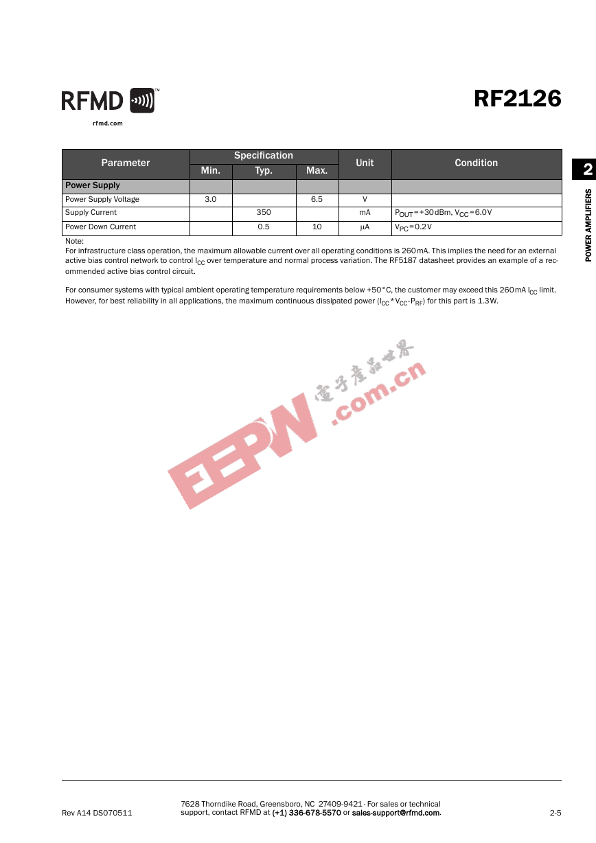
2POWER AMPLIFIERS2-5RF2126Rev A14 DS0705117628 Thorndike Road, Greensboro, NC 27409-9421 · For sales or technical support, contact RFMD at (+1) 336-678-5570 or sales-support@rfmd.com.ParameterSpecificationUnitConditionMin.Typ.Max.Power SupplyPower Supply Voltage3.06.5VSupply Current350mAPOUT=+30dBm, VCC=6.0VPower Down Current0.510μAVPC=0.2VNote: For infrastructure class operation, the maximum allowable current over all operating conditions is 260mA. This implies the need for an external active bias control network to control ICC over temperature and normal process variation. The RF5187 datasheet provides an example of a rec-ommended active bias control circuit.For consumer systems with typical ambient operating temperature requirements below +50°C, the customer may exceed this 260mA ICC limit. However, for best reliability in all applications, the maximum continuous dissipated power (ICC*VCC-PRF) for this part is 1.3W.�
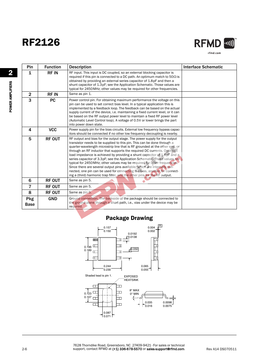
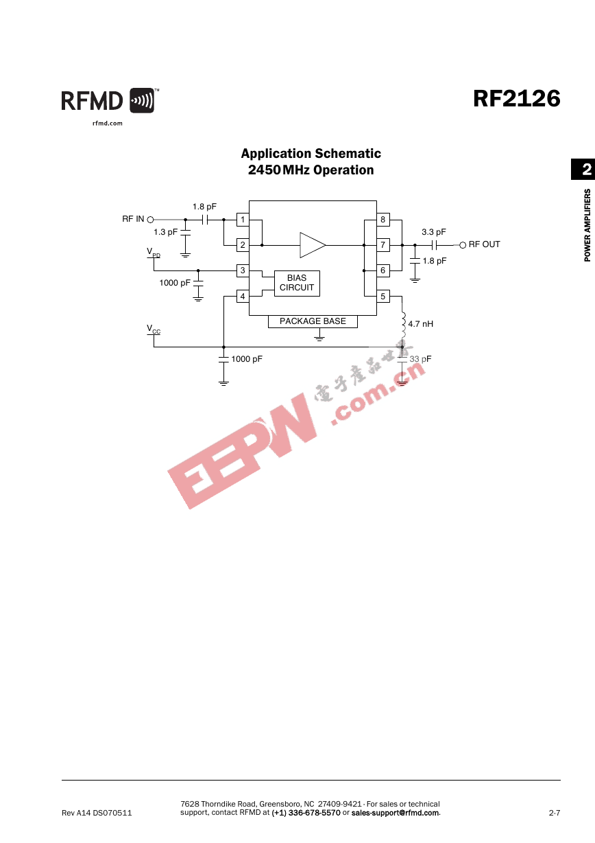
2POWER AMPLIFIERS2-6RF2126Rev A14 DS0705117628 Thorndike Road, Greensboro, NC 27409-9421 · For sales or technical support, contact RFMD at (+1) 336-678-5570 or sales-support@rfmd.com.Package DrawingPinFunctionDescriptionInterface Schematic1RF INRF input. This input is DC coupled, so an external blocking capacitor is required if this pin is connected to a DC path. An optimum match to 50Ω is obtained by providing an external series capacitor of 1.8pF and then a shunt capacitor of 1.3pF; see the Application Schematic. Those values are typical for 2450MHz; other values may be required for other frequencies.2RF INSame as pin 1.3PCPower control pin. For obtaining maximum performance the voltage on this pin can be used to set correct bias level. In a typical application this is implemented by a feedback loop. The feedback can be based on the actual supply current of the device, i.e. maintaining a fixed current level, or it can be based on the RF output power level to maintain a fixed RF power level (Automatic Level Control loop). A voltage of 0.5V or lower brings the part into power down state.4VCCPower supply pin for the bias circuits. External low frequency bypass capac-itors should be connected if no other low frequency decoupling is nearby.5RF OUTRF output and bias for the output stage. The power supply for the output transistor needs to be supplied to this pin. This can be done through a quarter-wavelength microstrip line that is RF grounded at the other end, or through an RF inductor that supports the required DC currents. Optimum load impedance is achieved by providing a shunt capacitor of 1.8pF and a series capacitor of 3.3pF; see the Application Schematic. Those values are typical for 2450MHz; other values may be required for other frequencies. Since there are several output pins available, which are internally con-nected, one pin can be used for connecting the bias, another for connect-ing a (third) harmonic trap filter, and the other pins for the RF output.6RF OUTSame as pin 5.7RF OUTSame as pin 5.8RF OUTSame as pin 5.Pkg BaseGNDGround connection. The backside of the package should be connected to the ground plane through a short path, i.e., vias under the device may be required.Shaded lead is pin 1.0.1570.1500.2440.2300.1960.1890.01920.01380.0500.0650.0550.0040.002-A-8° MAX0° MIN0.0350.0160.00980.00750.0870.0710.1230.107EXPOSEDHEATSINK�
2POWER AMPLIFIERS2-7RF2126Rev A14 DS0705117628 Thorndike Road, Greensboro, NC 27409-9421 · For sales or technical support, contact RFMD at (+1) 336-678-5570 or sales-support@rfmd.com.Application Schematic2450MHz Operation12348765BIASCIRCUITPACKAGE BASE4.7 nH1.8 pF1000 pF3.3 pF33 pF1000 pF1.3 pF1.8 pFVCCVPDRF INRF OUT�
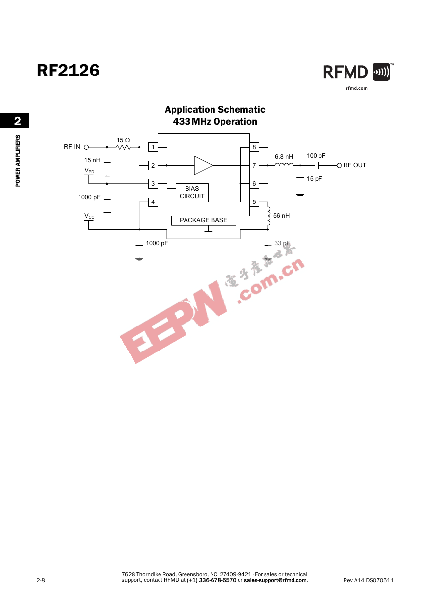
2POWER AMPLIFIERS2-8RF2126Rev A14 DS0705117628 Thorndike Road, Greensboro, NC 27409-9421 · For sales or technical support, contact RFMD at (+1) 336-678-5570 or sales-support@rfmd.com.Application Schematic433MHz Operation12348765BIASCIRCUITPACKAGE BASE56 nH15 pF1000 pF33 pF1000 pF15 nHVCCVPDRF INRF OUT15 Ω6.8 nH100 pF�
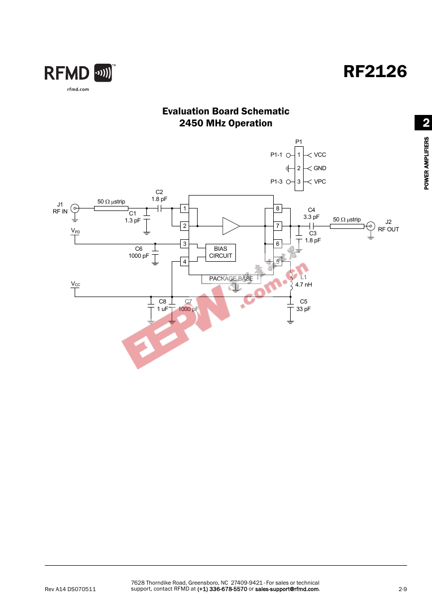
2POWER AMPLIFIERS2-9RF2126Rev A14 DS0705117628 Thorndike Road, Greensboro, NC 27409-9421 · For sales or technical support, contact RFMD at (+1) 336-678-5570 or sales-support@rfmd.com.Evaluation Board Schematic2450 MHz Operation 12348765BIASCIRCUITPACKAGE BASEL14.7 nHC31.8 pFC61000 pFC43.3 pFC533 pFC71000 pFC11.3 pFC21.8 pFVCCP1-1P1-3P1VPCGNDVCC123C81 uFJ1RF IN50 Ω μstripJ2RF OUT50 Ω μstripVPD�
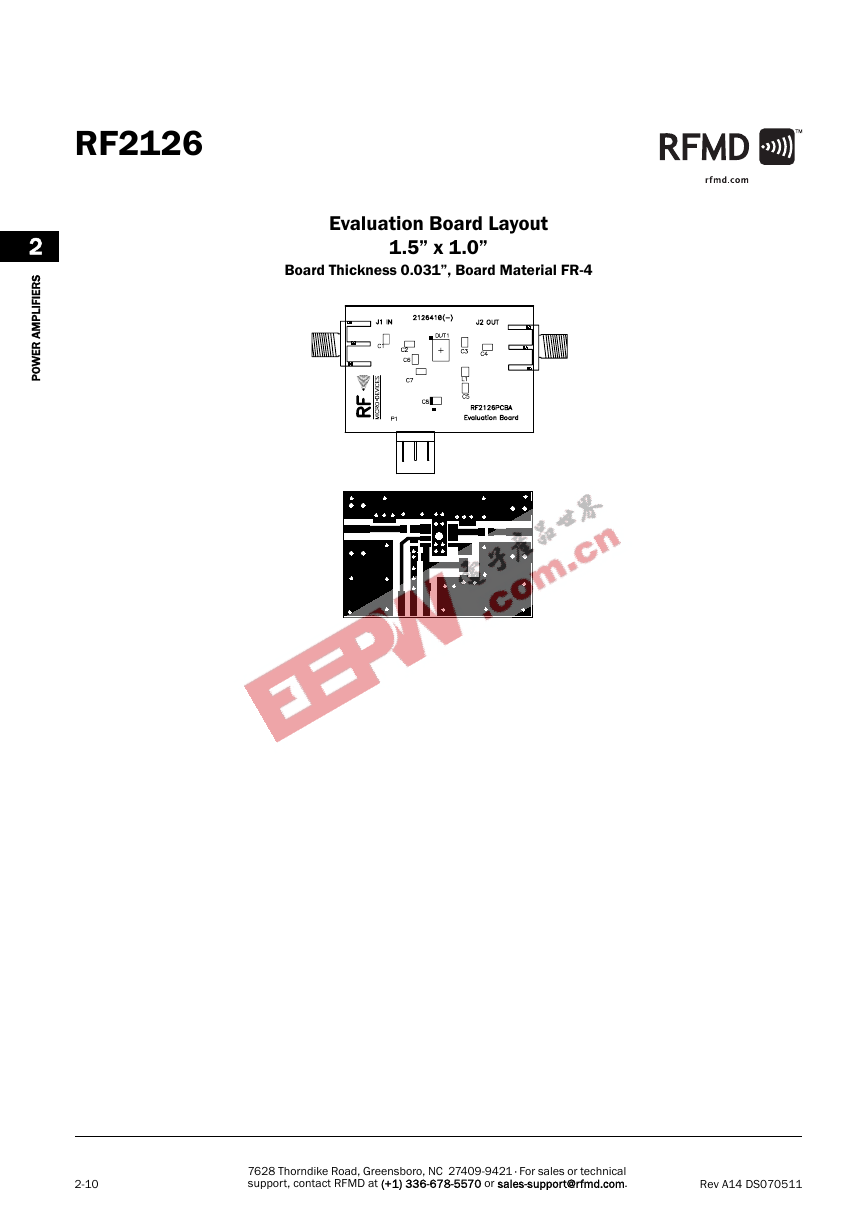
2POWER AMPLIFIERS2-10RF2126Rev A14 DS0705117628 Thorndike Road, Greensboro, NC 27409-9421 · For sales or technical support, contact RFMD at (+1) 336-678-5570 or sales-support@rfmd.com.Evaluation Board Layout1.5” x 1.0”Board Thickness 0.031”, Board Material FR-4�


 2023年江西萍乡中考道德与法治真题及答案.doc
 2012年重庆南川中考生物真题及答案.doc
 2013年江西师范大学地理学综合及文艺理论基础考研真题.doc
 2020年四川甘孜小升初语文真题及答案I卷.doc
 2020年注册岩土工程师专业基础考试真题及答案.doc
 2023-2024学年福建省厦门市九年级上学期数学月考试题及答案.doc
 2021-2022学年辽宁省沈阳市大东区九年级上学期语文期末试题及答案.doc
 2022-2023学年北京东城区初三第一学期物理期末试卷及答案.doc
 2018上半年江西教师资格初中地理学科知识与教学能力真题及答案.doc
 2012年河北国家公务员申论考试真题及答案-省级.doc
 2020-2021学年江苏省扬州市江都区邵樊片九年级上学期数学第一次质量检测试题及答案.doc
 2022下半年黑龙江教师资格证中学综合素质真题及答案.doc