logo资料库

sata3.0规范.pdf

第1页 / 共663页
第2页 / 共663页
第3页 / 共663页
第4页 / 共663页
第5页 / 共663页
第6页 / 共663页
第7页 / 共663页
第8页 / 共663页
资料共663页,剩余部分请下载后查看
TABLE OF CONTENTS
LIST OF FIGURES
LIST OF TABLES
1 Revision History
1.1 Revision 2.5 (Ratification Date October 27, 2005)
1.2 Revision 2.6 (Ratification Date February 15, 2007)
1.3 Revision 3.0 (Ratification Date: June 2, 2009)
2 Scope
3 Normative references
3.1 Approved references
3.2 References under development
3.3 Other references
4 Definitions, abbreviations, and conventions
4.1 Definitions and abbreviations
4.1.1 Active Port
4.1.2 ATA (AT Attachment)
4.1.3 ATAPI (AT Attachment Packet Interface) device
4.1.4 BER (bit error rate)
4.1.5 bitrate
4.1.6 bit synchronization
4.1.7 burst
4.1.8 byte
4.1.9 character
4.1.10 character alignment
4.1.11 character slipping
4.1.12 ClickConnect
4.1.13 CLTF (Closed Loop Transfer Function)
4.1.14 code violation
4.1.15 comma character
4.1.16 comma sequence
4.1.17 command aborted
4.1.18 command completion
4.1.19 command packet
4.1.20 concentrator
4.1.21 Control Block registers
4.1.22 control character
4.1.23 control port
4.1.24 control variable
4.1.25 CRC (Cyclic Redundancy Check)
4.1.26 data character
4.1.27 data signal source
4.1.28 device
4.1.29 device port
4.1.30 DCB (DC block)
4.1.31 differential signal
4.1.32 DJ (deterministic jitter – peak to peak)
4.1.33 DMA (direct memory access)
4.1.34 Dword
4.1.35 Dword synchronization
4.1.36 EMI (Electromagnetic Interference)
4.1.37 encoded character
4.1.38 endpoint device
4.1.39 elasticity buffer
4.1.40 eSATA
4.1.41 Fbaud
4.1.42 FER (frame error rate)
4.1.43 First-party DMA Data Phase
4.1.44 First-party DMA access
4.1.45 FIS (Frame Information Structure)
4.1.46 frame
4.1.47 Gen1
4.1.48 Gen1i
4.1.49 Gen1m
4.1.50 Gen1x
4.1.51 Gen2
4.1.52 Gen2i
4.1.53 Gen2m
4.1.54 Gen2x
4.1.55 Gen3
4.1.56 Gen3i
4.1.57 HBA (Host Bus Adapter)
4.1.58 HBWS (High Bandwidth Scope)
4.1.58.1 Gen1/Gen2 Requirement
4.1.58.2 Gen3 Requirement
4.1.59 HFTP (High Frequency Test Pattern)
4.1.60 hot plug
4.1.61 host port
4.1.62 inactive port
4.1.63 interrupt pending
4.1.64 immediate NCQ command
4.1.65 ISI (inter-symbol interference)
4.1.66 JMD (jitter measuring device)
4.1.67 JTF (Jitter Transfer Function)
4.1.68 junk
4.1.69 LBA (Logical Block Address)
4.1.70 LBP (Lone Bit Pattern)
4.1.71 LED (Light Emitting Diode)
4.1.72 legacy mode
4.1.73 legal character
4.1.74 LFSR (Linear Feedback Shift Register)
4.1.75 LFTP (low frequency test pattern)
4.1.76 LL (laboratory load)
4.1.77 LSS (laboratory sourced signal or lab-sourced signal)
4.1.78 MFTP (mid frequency test pattern)
4.1.79 NCQ streaming command
4.1.80 NCQ Non-streaming command
4.1.81 OOB (Out-of-Band signaling)
4.1.82 OS-aware hot plug
4.1.83 OS-aware hot removal
4.1.84 Phy offline
4.1.85 PIO (programmed input/output)
4.1.86 port address
4.1.87 PRD (Physical Region Descriptor)
4.1.88 primitive
4.1.89 protocol-based port selection
4.1.90 quiescent power condition
4.1.91 RJ (random jitter)
4.1.92 sector
4.1.93 SEMB (Serial ATA Enclosure Management Bridge)
4.1.94 SEP (Storage Enclosure Processor)
4.1.95 Shadow Register Block registers
4.1.96 side-band port selection
4.1.97 SMART
4.1.98 SSC (spread spectrum clocking)
4.1.99 surprise hot plug
4.1.100 surprise hot removal
4.1.101 SYNC Escape
4.1.102 TDR (time domain reflectometer)
4.1.103 TIA (timing interval analyzer)
4.1.104 TJ (total jitter)
4.1.105 UI (unit interval)
4.1.106 unrecoverable error
4.1.107 UUT (unit under test)
4.1.108 VNA (vector network analyzer)
4.1.109 warm plug
4.1.110 word
4.1.111 xSATA
4.1.112 zero crossing
4.2 Conventions
4.2.1 Precedence
4.2.2 Keywords
4.2.2.1 expected
4.2.2.2 mandatory
4.2.2.3 may
4.2.2.4 na
4.2.2.5 obsolete
4.2.2.6 optional
4.2.2.7 retired
4.2.2.8 reserved
4.2.2.9 shall
4.2.2.10 should
4.2.3 Numbering
4.2.4 Dimensions
4.2.5 Signal conventions
4.2.6 State machine conventions
4.2.7 Byte, word and Dword Relationships
5 General overview
5.1 Architecture
5.2 Usage Models
5.2.1 Internal 1 meter Cabled Host to Device
5.2.2 Short Backplane to Device
5.2.3 Long Backplane to Device
5.2.4 Internal 4-lane Cabled Disk Arrays
5.2.5 System-to-System Interconnects – Data Center Applications (xSATA)
5.2.6 System-to-System Interconnects – External Desktop Applications (eSATA)
5.2.7 Proprietary Serial ATA Disk Arrays
5.2.8 Serial ATA and SAS
5.2.9 Potential External SATA Incompatibility Issues
5.2.10 Mobile Applications
5.2.11 Port Multiplier Example Applications
6 Cables and Connectors
6.1 Internal cables and connectors
6.1.1 Internal Single Lane Description
6.1.1.1
6.1.2 Connector locations
6.1.3 Mating interfaces
6.1.3.1 Device plug connector
6.1.3.2 Pin Signal Definition and Contact Mating Sequence
6.1.4 Signal cable receptacle connector
6.1.5 Signal host plug connector
6.1.5.1 Internal plug stacking
6.1.6 Backplane connector
6.1.6.1 Backplane connector configuration and blind-mating tolerance
6.1.7 Power cable receptacle connector
6.1.8 Internal single lane cable
6.1.9 Connector labeling
6.1.10 Connector and cable assembly requirements and test procedures
6.1.10.1 Housing and contact electrical requirements
6.1.10.2 Mechanical and environmental requirements
6.1.10.3 Sample selection
6.1.10.4 Test sequence
6.1.11 Internal Multilane cables
6.1.11.1 Conformance Criteria
6.1.11.1.1 Electrical Requirements
6.1.11.1.2 Component Descriptions
6.1.11.1.3 Cable Receptacles and Backshells
6.1.11.2 4 Lane Pin Assignments
6.1.11.3 2 Lane Pin Assignments
6.1.12 Mini SATA Internal Multilane
6.1.12.1 Conformance Criteria
6.1.12.1.1 Electrical Requirements
6.1.12.1.2 Component Descriptions
6.1.12.1.3 Mechanical Requirements
6.1.12.2 Mini SATA Internal Multilane Pin Assignments
6.2 Internal Micro SATA Connector for 1.8” HDD
6.2.1 Usage model
6.2.2 General description
6.2.3 Connector location
6.2.4 Mating interfaces
6.2.4.1 Device internal micro SATA plug connector
6.2.4.2 Internal micro SATA backplane connector
6.2.4.3 Internal micro SATA power receptacle connector
6.2.4.4 Internal micro SATA connector pair blind-mate misalignment capability
6.2.4.5 Internal micro SATA pin signal definition and contact mating sequence
6.2.4.6 Internal micro SATA connector and cable assembly requirements and test procedures
6.3 Internal Slimline cables and connectors
6.3.1 Usage Models
6.3.2 General description
6.3.3 Connector location and keep out zones
6.3.3.1 Location
6.3.3.2 Keep out zones
6.3.3.2.1 9.5 mm Slimline Drives
6.3.3.2.2 12.7 mm Slimline Drives
6.3.4 Mating interfaces
6.3.4.1 7 mm Slimline Device plug connector
6.3.4.1.1 Connector pin signal definition
6.3.4.1.2 Housing and contact electrical and mechanical requirement
6.3.4.1.3 Connector and cable assembly requirements and test procedure
6.3.4.2 9.5 mm and 12.7 mm Slimline Device plug connector
6.3.4.2.1 Slimline Signal cable receptacle connector
6.3.4.2.2 Slimline Power cable receptacle connector
6.3.4.3 Slimline Host Receptacle Connector
6.3.5 Backplane connector configuration and blind-mating tolerance
6.3.6 Connector labeling
6.3.7 Connector and cable assembly requirements and test procedures
6.4 Internal LIF-SATA Connector for 1.8” HDD
6.4.1 General description
6.4.2 Connector Locations
6.4.2.1 Connector location on Hard Disk Drive (HDD) Form Factor, - (Reference)
6.4.2.2 Connector location on Solid State Drive (SSD) Form Factor, - (Reference)
6.4.3 Mating interfaces
6.4.3.1 Device internal LIF-SATA embedded type connector
Figure 87 defines the interface dimensions for the internal LIF-SATA embedded type connector with both signal and power segments.
6.4.3.2 Device internal LIF-SATA surface mounting type connector
Figure 88 defines the interface dimensions for the internal LIF-SATA device surface mounting type connector.
6.4.3.3 FPC for Internal LIF-SATA
6.4.4 Internal LIF-SATA pin signal definition and contact mating sequence
6.4.5 Housing and contact electrical requirement
6.5 External cables and connectors
6.5.1 External Single Lane
6.5.1.1 External Serial ATA Component General Descriptions
6.5.1.1.1 External Serial ATA Connector Mechanical drawings
6.5.1.2 External Serial ATA Electrical Requirements
6.5.1.3 External Serial ATA Mechanical Requirements
6.5.1.4 External Serial ATA Device Direct Connection Requirements
6.5.2 External Multilane
6.5.2.1 Multilane Cable Conformance Criteria
6.5.2.1.1 Electrical Parameters
6.5.2.1.2 Mechanical Parameters
6.5.2.2 Keying Requirements
6.5.2.3 4 Lane Pin Assignments
6.5.3 Mini SATA External Multilane
6.5.3.1 Conformance Criteria
6.5.3.1.1 Electrical Parameters
6.5.3.1.2 Mechanical Parameters
6.5.3.2 Mini SATA External Multilane Keying Requirements
6.5.3.3 Mini SATA External Multilane Pin Assignments
6.6 Cable and Connector Electrical Specifications
6.6.1 Serial ATA Cable
6.6.1.1 Electrical Requirements
6.6.2 Cable/Connector Test Methodology
6.6.2.1 Test Equipment
6.6.2.2 Test and Measurement Conditions
6.6.2.3 Test Fixture Considerations
6.6.2.4 Test Definition / Methodology
6.7 Power Segment Pin P11 Definition (Optional)
6.7.1 Device Activity Signal
6.7.1.1 Electrical Definition
6.7.1.2 LED Driver Circuit (Informative)
6.7.1.3 Functional Definition
6.7.2 Staggered Spin-up Disable Control
6.7.2.1 Electrical and Functional Definition
6.7.2.2 Staggered Spin-up Disable Circuit (Informative)
6.8 Precharge and Device Presence Detection
6.8.1 Device Requirements
6.8.2 Receptacle Precharge (Informative)
6.8.3 Presence Detection (Informative)
7 Phy Layer
7.1 Descriptions of Phy Electrical Specifications
7.1.1 List of Services
7.1.2 Low Level Electronics Block Diagrams (Informative)
7.1.2.1 Physical Plant Block Diagram
7.1.2.2 Analog Front End (AFE) Block Diagram Description
7.1.3 Compliance Testing
7.1.4 Link Performance
7.2 Electrical Specifications
7.2.1 Physical Layer Requirements Tables
7.2.2 Phy Layer Requirements Details
7.2.2.1 General Specifications Details
7.2.2.1.1 Channel Speed
7.2.2.1.2 Frame Error Rate
7.2.2.1.3 Unit Interval
7.2.2.1.4 TX Frequency Long Term Stability
7.2.2.1.5 Spread Spectrum Modulation Frequency
7.2.2.1.6 Spread Spectrum Modulation Deviation
7.2.2.1.7 DC Coupled Common Mode Voltage (Gen1i)
7.2.2.1.8 AC Coupled Common Mode Voltage
7.2.2.1.9 Nominal Differential Impedance (Gen1i)
7.2.2.1.10 AC Coupling Capacitance
7.2.2.1.11 Sequencing Transient Voltage
7.2.2.1.12 Sequencing Transient Voltage Lab Load (Gen3i)
7.2.2.2 Transmitter Specification Details
7.2.2.2.1 TX Pair Differential Impedance (Gen1i)
7.2.2.2.2 TX Single-Ended Impedance (Gen1i)
7.2.2.2.3 TX and RX Differential Mode Return Loss (Gen2i, Gen2m) (Gen1i, Gen1m alternate)
7.2.2.2.4 TX Common Mode Return Loss (Gen2i, Gen2m)
7.2.2.2.5 TX Impedance Balance (Gen2i, Gen2m, Gen3i)
7.2.2.2.6 TX and RX Differential Mode Return Loss (Gen3i)
7.2.2.2.7 TX Differential Output Voltage
7.2.2.2.8 TX Minimum Voltage Measurement Interval
7.2.2.2.9 TX Rise/Fall Time
7.2.2.2.10 TX Differential Skew
7.2.2.2.11 TX AC Common Mode Voltage (Gen2i, Gen1x, Gen2x)
7.2.2.2.12 TX AC Common Mode Voltage (Gen3i)
7.2.2.2.13 Common Mode Transient Settle Time (Gen1i)
7.2.2.2.14 OOB Differential Delta (Gen2i,Gen3i, Gen2m,Gen1x, Gen2x)
7.2.2.2.15 OOB Common Mode Delta (Gen2i, Gen3i,Gen1x, Gen2x)
7.2.2.2.16 TX Rise/Fall Imbalance
7.2.2.2.17 TX Amplitude Imbalance (Gen2i, Gen1x, Gen2x)
7.2.2.2.18 Clock-to-Data Transmit Jitter (Gen1i, Gen1m, Gen1x, Gen2i, Gen2m, Gen2x, Gen3i)
7.2.2.3 Receiver Specification Details
7.2.2.3.1 RX Pair Differential Impedance (Gen1i)
7.2.2.3.2 RX Single-Ended Impedance (Gen1i)
7.2.2.3.3 RX Differential Mode Return Loss (Gen2i, Gen2m)
7.2.2.3.4 RX Common Mode Return Loss (Gen2i, Gen2m)
7.2.2.3.5 RX Impedance Balance (Gen2i, Gen2m)
7.2.2.3.6 RX Differential Mode Return Loss (Gen3i)
7.2.2.4 Lab Load Details
7.2.2.5 Lab-Sourced Signal Details
7.2.2.5.1 RX Differential Input Voltage
7.2.2.5.2 RX Rise/Fall Times
7.2.2.5.3 RX Minimum Voltage Measurement Interval
7.2.2.5.4 RX Differential Skew (Gen2i, Gen1x, Gen2x, Gen3i)
7.2.2.5.5 RX AC Common Mode Voltage (Gen2i, Gen1x, Gen2x)
7.2.2.5.6 AC Common Mode Frequency
7.2.2.5.7 Clock-Data Receiver Jitter Tolerance (Gen1i, Gen1m, Gen2i, Gen2m, Gen1x, Gen2x)
7.2.2.5.8 Clock-Data Receiver Jitter Tolerance (Gen3i)
7.2.2.6 OOB Specifications Details
7.2.2.6.1 OOB Signal Burst Generation
7.2.2.6.2 OOB Signal Detection Threshold
7.2.2.6.3 UI During OOB Signaling (UIOOB)
7.2.2.6.4 COMINIT/COMRESET and COMWAKE Transmit Burst Length
7.2.2.6.5 COMINIT/COMRESET Transmit Gap Length
7.2.2.6.6 COMWAKE Transmit Gap Length
7.2.2.6.7 COMWAKE Gap Detection Windows
7.2.2.6.8 COMINIT/COMRESET Gap Detection Windows
7.2.3 Loopback
7.2.3.1 Far-End Retimed
7.2.3.2 Far-End Analog (Optional)
7.2.3.3 Near-End Analog (Optional)
7.2.4 Test Pattern Requirements
7.2.4.1 Non-Compliant Patterns
7.2.4.2 Compliant Frame Patterns
7.2.4.3 Test Bit Patterns and Sequence Characteristics
7.2.4.3.1 Low Transition Density Patterns (LTDP)
7.2.4.3.2 High Transition Density Patterns (HTDP)
7.2.4.3.3 Low Frequency Spectral Content Pattern (LFSCP)
7.2.4.3.4 Simultaneous Switching Outputs Pattern (SSOP)
7.2.4.3.5 Lone-Bit Pattern (LBP)
7.2.4.3.6 Composite Pattern (COMP)
7.2.5 Hot Plug Considerations
7.2.5.1 Hot Plug Overview
7.2.5.2 Electrical Requirements
7.2.5.3 Common-Mode Transients (Informative)
7.2.5.4 ESD (Informative)
7.2.5.5 Drive Body Discharge (Informative)
7.2.6 Mated Connector Pair Definition
7.2.7 Compliance Interconnect Channels (Gen1x, Gen2x, Gen3i)
7.2.7.1.1 Calibration of Compliance Interconnect Channels
7.2.8 Impedance Calibration (Optional)
7.3 Jitter
7.3.1 Jitter Definition
7.3.2 Reference Clock Definition
7.3.2.1 Gen1i, Gen1m, Gen2i and Gen2m Normative Requirements
7.3.2.2 Gen1i, Gen1m, Gen2i, and Gen2m Informative Comments
7.3.2.3 Gen1x and Gen2x Normative Requirements
7.3.2.4 Gen3i Normative Requirements
7.3.3 Spread Spectrum Clocking
7.3.4 Jitter Budget
7.4 Measurements
7.4.1 Frame Error Rate Testing
7.4.1.1 Frame Error Rate Patterns
7.4.1.2 Frame Error Rate Measurements
7.4.1.3 Amount of Data to Transfer to Achieve Target Confidence Level (Informative)
7.4.1.4 Bit Error Rate Testing (Informative)
7.4.1.4.1 Bit Error Rate Measurements
7.4.1.4.2 Amount of Data to Transfer to Achieve Target Error Rate
7.4.2 Measurement of Differential Voltage Amplitudes (Gen1, Gen2)
7.4.2.1 Testing for Minimum Differential Voltage Amplitude
7.4.2.1.1 Common Steps
7.4.2.1.2 Lone Bit Pattern Measurements, Option 1
7.4.2.1.3 Approximation to Lone Bit Pattern Measurements, Option 2
7.4.2.2 Test for Maximum Differential Voltage Amplitudes
7.4.3 Measurement of Differential Voltage Amplitudes (Gen3i)
7.4.3.1 Maximum Differential Voltage Amplitude (Gen3i)
7.4.3.2 Minimum Differential Voltage Amplitude (Gen3i)
7.4.4 Rise and Fall Times
7.4.5 Transmitter Amplitude
7.4.5.1 Transmitter Amplitude (Gen1 and Gen2)
7.4.5.2 Transmitter Amplitude (Gen3i)
7.4.6 Receive Amplitude
7.4.7 Long Term Frequency Accuracy
7.4.8 Jitter Measurements
7.4.8.1 Jitter Measurements with a Bit Error Rate Tester (BERT)
7.4.9 Transmit Jitter (Gen1i, Gen2i, Gen1m, Gen2m, Gen1x, and Gen2x)
7.4.10 Transmit Jitter (Gen3i)
7.4.11 Receiver Tolerance (Gen1i, Gen2i, Gen1m, Gen2m, Gen1x, and Gen2x)
7.4.12 Receiver Tolerance (Gen3i)
7.4.13 Return Loss and Impedance Balance
7.4.14 SSC Profile
7.4.15 Intra-Pair Skew
7.4.16 Sequencing Transient Voltage
7.4.17 AC Coupling Capacitor
7.4.18 TX Amplitude Imbalance
7.4.19 TX Rise/Fall Imbalance
7.4.20 TX AC Common Mode Voltage (Gen2i, Gen2m)
7.4.21 Tx AC Common Mode Voltage (Gen3i)
7.4.22 OOB Common Mode Delta
7.4.23 OOB Differential Delta
7.4.24 Squelch Detector Tests
7.4.25 OOB Signaling Tests
7.4.25.1 Power-On Sequence
7.4.25.1.1 Calibration
7.4.25.1.2 Speed Negotiation
7.4.25.1.3 Interface Power Management Sequences
7.4.25.1.4 Partial
7.4.25.1.5 Slumber
7.4.26 TDR Differential Impedance (Gen1i / Gen1m)
7.4.27 TDR Single-Ended Impedance (Gen1i / Gen1m)
7.4.28 DC Coupled Common Mode Voltage (Gen1i / Gen1m)
7.4.29 AC Coupled Common Mode Voltage (Gen1i / Gen1m)
7.4.30 Sequencing Transient Voltage - Laboratory Load (Gen3i)
7.5 Interface States
7.5.1 Out Of Band Signaling
7.5.1.1 Idle Bus Status
7.5.1.2 COMRESET
7.5.1.3 COMINIT
7.5.1.4 COMWAKE
7.5.1.5 Design Example (Informative)
7.5.2 Idle Bus Condition
7.6 Elasticity Buffer Management
8 OOB and Phy Power States
8.1 Interface Power States
8.2 Asynchronous Signal Recovery (Optional)
8.2.1 Unsolicited COMINIT Usage (Informative)
8.3 OOB and Signature FIS return (Informative)
8.4 Power-On Sequence State Machine
8.4.1 Host Phy Initialization State Machine
8.4.2 Device Phy Initialization State Machine
8.4.3 Speed Negotiation
8.4.3.1 Power-On Sequence Timing Diagram
8.4.3.2 Partial/Slumber to PHYRDY
8.4.3.2.1 Host Initiated
8.4.3.2.2 Device Initiated
8.4.3.3 PHYRDY to Partial/Slumber
8.4.3.3.1 Host Initiated
8.4.3.3.2 Device Initiated
9 Link Layer
9.1 Overview
9.1.1 Frame Transmission
9.1.2 Frame Reception
9.2 Encoding Method
9.2.1 Notation and Conventions
9.2.2 Character Code
9.2.2.1 Code Construction
9.2.2.2 The Concept of Running Disparity
9.2.2.3 Data Encoding
9.2.2.4 Encoding Examples
9.2.2.5 8b/10b Valid Encoded Characters
9.2.2.5.1 Data Characters
9.2.2.5.2 Control Characters
9.2.3 Transmission Summary
9.2.3.1 Transmission Order
9.2.3.1.1 Bits Within a Byte
9.2.3.1.2 Bytes Within a Dword
9.2.3.1.3 Dwords Within a Frame
9.2.4 Reception Summary
9.2.4.1 Disparity and the Detection of a Code Violation
9.3 Transmission Overview
9.4 Primitives
9.4.1 Overview
9.4.1.1 Primitive Disparity
9.4.1.2 Primitive Handshakes
9.4.2 Primitive Descriptions
9.4.3 Primitive Encoding
9.4.4 DMATP Primitive
9.4.5 CONTP Primitive
9.4.5.1 Scrambling of Data Following the CONTP Primitive
9.4.5.2 Periodic Retransmission of Sustained Primitives (Informative)
9.4.6 ALIGNP Primitive
9.4.7 Flow Control Signaling Latency
9.4.7.1 Cable Length and Flow Control Latency (Informative)
9.4.8 Examples of Primitive Usage (Informative)
9.5 CRC and Scrambling
9.5.1 Relationship Between Scrambling of FIS Data and Repeated Primitives
9.5.2 Relationship Between Scrambling and CRC
9.5.3 Scrambling Disable (Informative)
9.6 Link Layer State Machine
9.6.1 Terms Used in Link Layer Transition Tables
9.6.2 Link Idle State Diagram
9.6.3 Link Transmit State Diagram
9.6.4 Link Receive State Diagram
9.6.5 Link Power Mode State Diagram
10 Transport Layer
10.1 Overview
10.1.1 FIS construction
10.1.2 FIS decomposition
10.2 Frame Information Structure (FIS)
10.2.1 Overview
10.2.2 Payload content
10.3 FIS Types
10.3.1 FIS Type values
10.3.1.1 Unrecognized FIS Types
10.3.2 CRC Errors on Data FISes
10.3.3 All FIS types
10.3.4 Register - Host to Device
10.3.4.1 Description
10.3.4.2 Transmission
10.3.4.3 Reception
10.3.5 Register - Device to Host
10.3.5.1 Description
10.3.5.2 Transmission
10.3.5.3 Reception
10.3.6 Set Device Bits - Device to Host
10.3.6.1 Description
10.3.6.2 Transmission
10.3.6.3 Reception
10.3.7 DMA Activate - Device to Host
10.3.7.1 Description
10.3.7.2 Transmission
10.3.7.3 Reception
10.3.8 DMA Setup – Device to Host or Host to Device (Bidirectional)
10.3.8.1 Description
10.3.8.2 Transmission
10.3.8.3 Reception
10.3.8.3.1 Auto-Activate
10.3.8.4 HBA Enforcement of First-party DMA Data Phase Atomicity
10.3.9 BIST Activate - Bidirectional
10.3.9.1 Description
10.3.9.2 Transmission
10.3.9.3 Reception
10.3.10 PIO Setup – Device to Host
10.3.10.1 Description
10.3.10.2 Transmission of PIO Setup by Device Prior to a Data Transfer from Host to Device
10.3.10.3 Reception of PIO Setup by Host Prior to a Data Transfer from Host to Device
10.3.10.4 Transmission of PIO Setup by Device Prior to a Data Transfer from Device to Host
10.3.10.5 Reception of PIO Setup by Host Prior to a Data Transfer from Device to Host
10.3.11 Data - Host to Device or Device to Host (Bidirectional)
10.3.11.1 Description
10.3.11.2 Transmission
10.3.11.3 Reception
10.4 Host transport states
10.4.1 Host transport idle state diagram
10.4.2 Host Transport transmit command FIS diagram
10.4.3 Host Transport transmit control FIS diagram
10.4.4 Host Transport transmit DMA Setup – Device to Host or Host to Device FIS state diagram
10.4.5 Host Transport transmit BIST Activate FIS
10.4.6 Host Transport decomposes Register FIS diagram
10.4.7 Host Transport decomposes a Set Device Bits FIS state diagram
10.4.8 Host Transport decomposes a DMA Activate FIS diagram
10.4.9 Host Transport decomposes a PIO Setup FIS state diagram
10.4.10 Host Transport decomposes a DMA Setup FIS state diagram
10.4.11 Host transport decomposes a BIST Activate FIS state diagram
10.5 Device transport states
10.5.1 Device transport idle state diagram
10.5.2 Device Transport sends Register – Device to Host state diagram
10.5.3 Device Transport sends Set Device Bits FIS state diagram
10.5.4 Device Transport transmit PIO Setup – Device to Host FIS state diagram
10.5.5 Device Transport transmit DMA Activate FIS state diagram
10.5.6 Device Transport transmit DMA Setup – Device to Host FIS state diagram
10.5.7 Device Transport transmit Data – Device to Host FIS diagram
10.5.8 Device Transport transmit BIST Activate FIS diagram
10.5.9 Device Transport decomposes Register – Host to Device state diagram
10.5.10 Device Transport decomposes Data (Host to Device) FIS state diagram
10.5.11 Device Transport decomposes DMA Setup – Host to Device state diagram
10.5.12 Device Transport decomposes a BIST Activate FIS state diagram
11 Device Command Layer protocol
11.1 Power-on and COMRESET protocol
11.2 Device Idle protocol
11.3 Software reset protocol
11.4 EXECUTE DEVICE DIAGNOSTIC command protocol
11.5 DEVICE RESET command protocol
11.6 Non-data command protocol
11.7 PIO data-in command protocol
11.8 PIO data-out command protocol
11.9 DMA data in command protocol
11.10 DMA data out command protocol
11.11 PACKET protocol
11.12 READ DMA QUEUED command protocol
11.13 WRITE DMA QUEUED command protocol
11.14 FPDMA QUEUED command protocol
12 Host Command Layer protocol
12.1 FPDMA QUEUED command protocol
13 Application Layer
13.1 Parallel ATA Emulation
13.1.1 Software Reset
13.1.2 Master-only emulation
13.1.3 Master/Slave emulation (optional)
13.1.3.1 Software reset
13.1.3.2 EXECUTE DEVICE DIAGNOSTICS
13.1.3.3 Restrictions and limitations
13.1.3.4 Shadow Command Block Register Access Restrictions
13.1.3.5 Parallel ATA interoperability state diagrams
13.2 IDENTIFY (PACKET) DEVICE
13.2.1 IDENTIFY DEVICE
13.2.1.1 Word 0 - 46: Set as indicated in ATA8-ACS
13.2.1.2 Word 47: Multiword PIO transfer
13.2.1.3 Word 48: Set as indicated in ATA8-ACS
13.2.1.4 Word 49: Capabilities
13.2.1.5 Words 50 - 52: Set as indicated in ATA8-ACS
13.2.1.6 Word 53: Field validity
13.2.1.7 Word 54 - 62: Set as indicated in ATA8-ACS
13.2.1.8 Word 63: Multiword DMA transfer
13.2.1.9 Word 64: PIO transfer modes supported
13.2.1.10 Word 65: Minimum Multiword DMA transfer cycle time per word
13.2.1.11 Word 66: Device recommended Multiword DMA cycle time
13.2.1.12 Word 67: Minimum PIO transfer cycle time without flow control
13.2.1.13 Word 68: Minimum PIO transfer cycle time with IORDY
13.2.1.14 Words 69-74: Set as indicated in ATA8-ACS
13.2.1.15 Word 75: Queue depth
13.2.1.16 Word 76: Serial ATA capabilities
13.2.1.17 Word 77: Serial ATA Additional capabilities
13.2.1.18 Word 78: Serial ATA features supported
13.2.1.19 Word 79: Serial ATA features enabled
13.2.1.20 Words 80-87: Set as indicated in ATA8-ACS
13.2.1.21 Word 88: Ultra DMA modes
13.2.1.22 Words 89 - 92: Set as indicated in ATA8-ACS
13.2.1.23 Word 93: Hardware configuration test results
13.2.1.24 Words 94-221: Set as indicated in ATA8-ACS.
13.2.1.25 Word 222: Transport Major Revision
13.2.1.26 Word 223: Transport Minor Revision
13.2.1.27 Words 224-255: Set as indicated in ATA8-ACS.
13.2.2 IDENTIFY PACKET DEVICE
13.2.2.1 Word 0 - 48: Set as indicated in ATA8-ACS
13.2.2.2 Word 49: Capabilities
13.2.2.3 Words 50 - 52: Set as indicated in ATA8-ACS
13.2.2.4 Word 53: Field validity
13.2.2.5 Word 54 - 62: Set as indicated in ATA8-ACS
13.2.2.6 Word 63: Multiword DMA transfer
13.2.2.7 Word 64: PIO transfer modes supported
13.2.2.8 Word 65: Minimum Multiword DMA transfer cycle time per word
13.2.2.9 Word 66: Device recommended Multiword DMA cycle time
13.2.2.10 Word 67: Minimum PIO transfer cycle time without flow control
13.2.2.11 Word 68: Minimum PIO transfer cycle time with IORDY
13.2.2.12 Words 69-75: Set as indicated in ATA8-ACS
13.2.2.13 Word 76: Serial ATA capabilities
13.2.2.14 Word 77: Serial ATA Additional capabilities
13.2.2.15 Word 78: Serial ATA features supported
13.2.2.16 Word 79: Serial ATA features enabled
13.2.2.17 Words 80-87: Set as indicated in ATA8-ACS
13.2.2.18 Word 88: Ultra DMA modes
13.2.2.19 Word 89 - 92: Set as indicated in ATA8-ACS
13.2.2.20 Word 93: Hardware configuration test results
13.2.2.21 Words 94-221: Set as indicated in ATA8-ACS.
13.2.2.22 Word 222: Transport Major Revision
13.2.2.23 Word 223: Transport Minor Revision
13.2.2.24 Words 224-255: Set as indicated in ATA8-ACS.
13.2.3 Determining Support for Serial ATA Features
13.3 SET FEATURES
13.3.1 Enable/Disable Non-Zero Offsets in DMA Setup
13.3.2 Enable/Disable DMA Setup FIS Auto-Activate Optimization
13.3.3 Enable/Disable Device-Initiated Interface Power State Transitions
13.3.4 Enable/Disable Guaranteed in-Order Data Delivery
13.3.5 Enable/Disable Asynchronous Notification
13.3.6 Enable/Disable Software Settings Preservation
13.3.7 Enable/Disable Device Automatic Partial to Slumber Transitions
13.4 Device Configuration Overlay
13.4.1 Device Configuration Overlay Identify
13.4.2 Device Configuration Overlay Set
13.5 Software Settings Preservation (Optional)
13.5.1 Warm Reboot Considerations (Informative)
13.6 Native Command Queuing (Optional)
13.6.1 Definition
13.6.1.1 Command Issue Mechanism
13.6.1.2 Data Delivery Mechanism
13.6.1.3 Status Return Mechanism
13.6.1.4 Priority
13.6.1.5 Unload
13.6.2 Intermixing Non-Native Queued Commands and Native Queued Commands
13.6.3 Command Definitions
13.6.3.1 READ FPDMA QUEUED
13.6.3.2 Success Outputs
13.6.3.3 Error Outputs
13.6.3.3.1.1 Upon receipt of a command
13.6.3.3.1.2 During execution of a command
13.6.3.4 Queue abort
13.6.3.5 WRITE FPDMA QUEUED
13.6.3.6 Success Outputs
13.6.3.7 Error Outputs
13.6.3.7.1.1 Upon receipt of a command
13.6.3.7.1.2 During execution of a command
13.6.3.8 NCQ QUEUE MANAGEMENT
13.6.3.8.1 ABORT NCQ QUEUE Subcommand ( 0h )
13.6.3.8.1.1 Success Outputs
13.6.3.8.1.2 Error Outputs
13.6.3.8.1.2.1 Upon receipt of a command
13.6.3.8.1.2.2 During execution of a command
13.6.3.8.2 Deadline Handling Subcommand ( 1h )
13.6.3.8.2.1 Success Outputs
13.6.3.8.2.2 Error Outputs
13.6.3.8.2.2.1 Upon receipt of a command
13.6.3.8.2.2.2 During execution of a command
13.6.4 First-party DMA HBA Support (Informative)
13.7 SATA Logs
13.7.1 Log Address Definitions
13.7.2 General Purpose Log Directory (00h)
13.7.3 Queued Error Log (10h)
13.7.4 Phy Event Counters Log (11h)
13.7.5 NCQ Queue Management Log (12h)
13.8 Asynchronous Notification (Optional)
13.8.1 Set Device Bits FIS Notification bit
13.8.2 Notification Mechanism
13.8.3 State Diagram for Asynchronous Notification
13.8.4 ATAPI Notification
13.8.4.1 Event Example (Informative)
13.9 Phy Event Counters (Optional)
13.9.1 Counter Reset Mechanisms
13.9.2 Counter Identifiers
13.9.2.1 Counter Definitions
13.9.2.1.1 Identifier 000h
13.9.2.1.2 Identifier 001h
13.9.2.1.3 Identifier 002h
13.9.2.1.4 Identifier 003h
13.9.2.1.5 Identifier 004h
13.9.2.1.6 Identifier 005h
13.9.2.1.7 Identifier 006h
13.9.2.1.8 Identifier 007h
13.9.2.1.9 Identifier 008h
13.9.2.1.10 Identifier 009h
13.9.2.1.11 Identifier 00Ah
13.9.2.1.12 Identifier 00Bh
13.9.2.1.13 Identifier 00Dh
13.9.2.1.14 Identifier 00Fh
13.9.2.1.15 Identifier 010h
13.9.2.1.16 Identifier 012h
13.9.2.1.17 Identifier 013h
13.9.3 Phy Event Counters Log (11h)
13.10 Staggered Spin-up (Optional)
13.11 Non-512 Byte Sector Size (Informative)
13.12 Defect Management (Informative)
13.12.1 Overview (Informative)
13.12.2 Typical Serial ATA Reliability Metrics (Informative)
13.12.3 An Overview of Serial ATA Defect Management (Informative)
13.12.4 Continuous Background Defect Scanning (Informative)
13.12.5 Self-Monitoring, Analysis and Reporting Technology (Informative)
13.13 Enclosure Services/Management (Optional)
13.13.1 Overview
13.13.2 Topology
13.13.2.1 Definition Configuration
13.13.3 Limitations
13.13.4 Definition
13.13.4.1 Discovery
13.13.4.2 Logical Command Block Registers to I2C Mapping
13.13.4.2.1 Command Delivery
13.13.4.2.2 Status Mechanism
13.13.4.3 Host-to-SEP Data Commands
13.13.4.4 SEP-to-Host Data Commands
13.13.5 SES and SAF-TE Extensions
13.13.5.1 IDENTIFY SEP Command (ECh)
13.13.5.1.1 IDENTIFY SEP Data Structure
13.13.5.2 Activity LED Control
13.13.5.2.1 SAF-TE - Write Device Slot Status Modification
13.13.5.2.2 SES- Device Element Definition Modification
13.13.5.2.3 Activity Indication Behavior and Operation
13.13.5.3 Slot – to – Port Correspondence
13.13.5.3.1 SAF-TE Correspondence Definition (Optional)
13.13.5.3.2 SES Correspondence Definition (Optional)
13.13.6 Enclosure Services Hardware Interface
13.13.6.1 I2C Cable/Connector definition
13.13.6.2 SEP Discovery and Enumeration
13.14 HDD Activity Indication (Optional)
13.14.1 HDD Activity Emulation of Desktop Behavior
13.14.1.1 Desktop HDD Activity Signal Electrical Requirements
13.14.2 Activity/Status Indication Reference (Informative)
13.15 Port Multiplier Discovery and Enumeration
13.15.1 Power-up
13.15.2 Resets
13.15.2.1 COMRESET
13.15.2.2 Software Reset
13.15.2.3 Device Reset
13.15.3 Software Initialization Sequences (Informative)
13.15.3.1 Port Multiplier Aware Software
13.15.3.2 Non-Port Multiplier Aware Software
13.15.3.3 Boot Devices Connected to Port Multiplier
13.15.4 Port Multiplier Discovery and Device Enumeration (Informative)
13.15.4.1 Port Multiplier Discovery
13.15.4.1.1 Considerations when Port Multiplier Not Present
13.15.4.2 Device Enumeration
13.16 Automatic Partial to Slumber Transitions
14 Host adapter register interface
14.1 Status and Control Registers
14.1.1 SStatus register
14.1.2 SError register
14.1.3 SControl register
14.1.4 SActive register
14.1.5 SNotification register (Optional)
15 Error handling
15.1 Architecture
15.2 Phy error handling overview
15.2.1 Error detection
15.2.2 Error control actions
15.2.2.1 No device present
15.2.2.2 OOB signaling sequence failure
15.2.2.3 Phy internal error
15.2.3 Error reporting
15.3 Link layer error handling overview
15.3.1 Error detection
15.3.2 Error control actions
15.3.2.1 Invalid state transitions
15.3.3 Error reporting
15.4 Transport layer error handling overview
15.4.1 Error detection
15.4.2 Error control actions
15.4.2.1 Internal errors
15.4.2.2 Frame errors
15.4.2.3 Protocol and state transition errors
15.4.3 Error reporting
15.5 Application layer error handling overview
15.5.1 Error detection
15.5.2 Error control actions
16 Port Multiplier
16.1 Introduction
16.2 Overview
16.3 Definition
16.3.1 Addressing Mechanism
16.3.2 Device Port Requirements
16.3.2.1 Transmission from Host to Device
16.3.2.2 Transmission from Device to Host
16.3.3 Policies
16.3.3.1 FIS Delivery
16.3.3.1.1 Port Priority
16.3.3.1.2 FIS Delivery Mechanisms (Informative)
16.3.3.2 Collisions
16.3.3.3 Booting with Software That Is Not Port Multiplier Aware
16.3.3.4 Staggered Spin-Up Support
16.3.3.5 Hot Plug Events
16.3.3.5.1 Hot Plug State Machine for Host Port
16.3.3.5.2 Hot Plug State Machine for Device Port
16.3.3.6 Link Power Management
16.3.3.7 Reducing Context Switching Complexity
16.3.3.8 Error Handling and Recovery
16.3.3.8.1 Command Timeout
16.3.3.8.2 Disabled Device Port
16.3.3.8.3 Invalid Device Port Address
16.3.3.8.4 Invalid CRC for Device Initiated Transfer
16.3.3.8.5 Data Corruption
16.3.3.8.6 Unsupported Command Received on Control Port
16.3.3.9 BIST Support
16.3.3.10 Asynchronous Notification
16.3.3.10.1 Command-Based Switching (Informative)
16.3.3.11 Phy Event Counters
16.3.3.11.1 Counter Identifiers
16.3.3.11.2 Reading Counter Values
16.3.3.11.3 Counter Reset Mechanisms
16.4 Port Multiplier Registers
16.4.1 General Status and Control Registers
16.4.1.1 Static Configuration Information
16.4.1.2 Status Information and Control
16.4.1.3 Features Supported
16.4.1.4 Features Enabled
16.4.1.5 Vendor Unique
16.4.1.6 Phy Event Counters
16.4.1.7 Reserved
16.4.2 Port Status and Control Registers
16.4.2.1 Phy Event Counters
16.5 Port Multiplier Command Definitions
16.5.1 READ PORT MULTIPLIER
16.5.1.1 Inputs
16.5.1.2 Success Outputs
16.5.1.3 Error Outputs
16.5.2 WRITE PORT MULTIPLIER
16.5.2.1 Inputs
16.5.2.2 Success Outputs
16.5.2.3 Error Outputs
16.5.3 Interrupts
16.6 Controlling PM Port Value and Interface Power Management
16.7 Switching Types (Informative)
16.7.1 Command-Based Switching
16.7.2 FIS-Based Switching
16.7.2.1 Host Controller Requirements
17 Port Selector
17.1 Example Applications
17.2 Overview
17.3 Active Port Selection
17.3.1 Protocol-based Port Selection
17.3.1.1 Port Selection Signal Definition
17.3.1.2 Presence Detection
17.3.1.2.1 Host port Phy state machine enhancements
17.3.1.2.2 Host Phy Initialization state machine impact (Informative)
17.3.1.2.3 SError Register Enhancement for Presence Detection
17.3.1.3 Host Transmission Considerations (Informative)
17.3.2 Side-band Port Selection
17.3.3 Behavior during a change of active port
17.3.3.1 Device State after a change of active port (Informative)
17.4 Behavior and Policies
17.4.1 Control State Machine
17.4.2 BIST support
17.4.3 Flow control signaling latency
17.4.4 Power Management
17.4.4.1 Wakeup Budget
17.4.5 OOB Phy signals
17.4.6 Hot Plug
17.4.7 Speed Negotiation
17.4.8 Spread spectrum clocking
17.5 Power-up and Resets
17.5.1 Power-up
17.5.1.1 Presence detection of Port Selector
17.5.2 Resets
17.5.2.1 COMRESET
17.5.2.2 Software reset and DEVICE RESET
17.6 Host Implementation (Informative)
17.6.1 Software Method for Protocol-based Selection (Informative)
Appendix A. Sample Code for CRC and Scrambling(Informative)
Appendix B. Command processing overview (Informative)
Appendix C. Device Emulation of nIEN with Interrupt Pending(Informative)
Appendix D. I/O Controller Module (Informative)
Appendix E. Jitter Formulas without SSC (Informative)
HIGH SPEED SERIALIZED AT ATTACHMENT Serial ATA International Organization Serial ATA International Organization: Serial ATA Revision 3.0 June 2, 2009 Gold Revision SATA-IO Board Members: Dell Computer Corporation Hewlett Packard Corporation Hitachi Global Storage Technologies, Inc. Intel Corporation Maxim Integrated Products Seagate Technology Western Digital Corporation Serial ATA Revision 3.0 - Gold Revision
SPECIFICATION DISCLAIMER “AS Serial ATA International Organization: Serial ATA Revision 3.0 specification ("Final Specification") is available for download at www.sata-io.org. IS PROVIDED TO YOU THIS SPECIFICATION IS” WITH NO WARRANTIES WHATSOEVER, INCLUDING ANY WARRANTY OF MERCHANTABILITY, NON- INFRINGEMENT, OR FITNESS FOR ANY PARTICULAR PURPOSE. THE AUTHORS OF THIS SPECIFICATION DISCLAIM ALL LIABILITY, INCLUDING LIABILITY FOR INFRINGEMENT OF ANY PROPRIETARY RIGHTS, RELATING TO USE OR IMPLEMNETATION OF INFORMATION IN THIS SPECIFICATION. THE AUTHORS DO NOT WARRANT OR REPRESENT THAT SUCH USE WILL NOT INFRINGE SUCH RIGHTS. THE PROVISION OF THIS SPECIFICATION TO YOU DOES NOT PROVIDE YOU WITH ANY LICENSE, EXPRESS OR IMPLIED, BY ESTOPPEL OR OTHERWISE, TO ANY INTELLECTUAL PROPERTY RIGHTS. Copyright 2002-2009, Serial ATA International Organization. All rights reserved. For more information about Serial ATA, refer to the Serial ATA International Organization website at www.sata-io.org. All product names are trademarks, registered trademarks, or servicemarks of their respective owners. Serial ATA International Organization contact information: SATA-IO 3855 SW 153rd Drive Beaverton, Oregon 97006 USA Tel: +1 503-619-0572 Fax: +1 503-644-6708 E-mail: admin@sata-io.org Serial ATA Revision 3.0 Gold Revision page 2 of 663
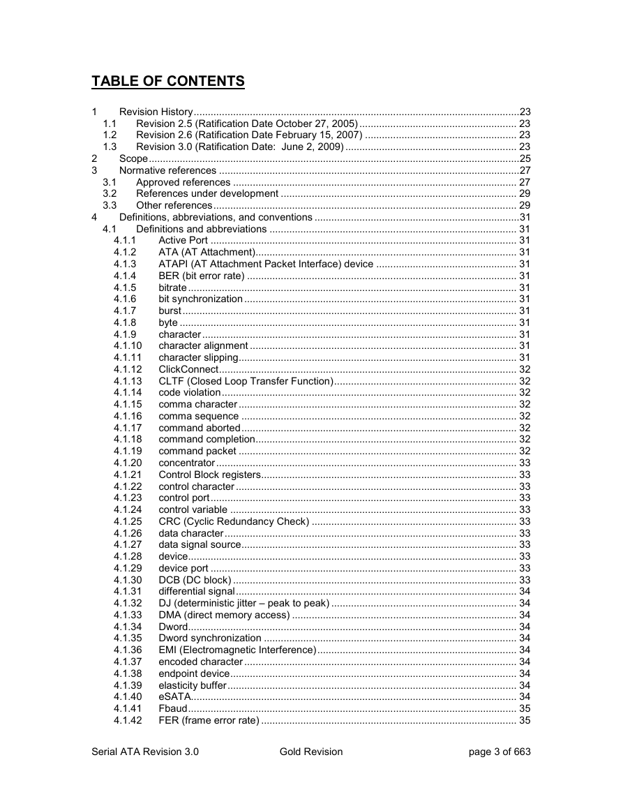
TABLE OF CONTENTS 1 2 3 4 1.1 1.2 1.3 3.1 3.2 3.3 4.1 Revision History....................................................................................................................23 Revision 2.5 (Ratification Date October 27, 2005) ........................................................ 23 Revision 2.6 (Ratification Date February 15, 2007) ...................................................... 23 Revision 3.0 (Ratification Date: June 2, 2009) ............................................................. 23 Scope....................................................................................................................................25 Normative references ...........................................................................................................27 Approved references ..................................................................................................... 27 References under development .................................................................................... 29 Other references............................................................................................................ 29 Definitions, abbreviations, and conventions .........................................................................31 Definitions and abbreviations ........................................................................................ 31 Active Port ............................................................................................................. 31 4.1.1 ATA (AT Attachment)............................................................................................. 31 4.1.2 4.1.3 ATAPI (AT Attachment Packet Interface) device .................................................. 31 4.1.4 BER (bit error rate) ................................................................................................ 31 4.1.5 bitrate..................................................................................................................... 31 bit synchronization ................................................................................................. 31 4.1.6 4.1.7 burst....................................................................................................................... 31 4.1.8 byte ........................................................................................................................ 31 4.1.9 character................................................................................................................ 31 4.1.10 character alignment ............................................................................................... 31 4.1.11 character slipping................................................................................................... 31 4.1.12 ClickConnect.......................................................................................................... 32 4.1.13 CLTF (Closed Loop Transfer Function)................................................................. 32 4.1.14 code violation......................................................................................................... 32 comma character ................................................................................................... 32 4.1.15 4.1.16 comma sequence .................................................................................................. 32 4.1.17 command aborted.................................................................................................. 32 4.1.18 command completion............................................................................................. 32 4.1.19 command packet ................................................................................................... 32 concentrator........................................................................................................... 33 4.1.20 4.1.21 Control Block registers........................................................................................... 33 4.1.22 control character .................................................................................................... 33 4.1.23 control port............................................................................................................. 33 control variable ...................................................................................................... 33 4.1.24 4.1.25 CRC (Cyclic Redundancy Check) ......................................................................... 33 4.1.26 data character........................................................................................................ 33 4.1.27 data signal source.................................................................................................. 33 4.1.28 device..................................................................................................................... 33 4.1.29 device port ............................................................................................................. 33 4.1.30 DCB (DC block) ..................................................................................................... 33 4.1.31 differential signal.................................................................................................... 34 4.1.32 DJ (deterministic jitter – peak to peak) .................................................................. 34 4.1.33 DMA (direct memory access) ................................................................................ 34 4.1.34 Dword..................................................................................................................... 34 4.1.35 Dword synchronization .......................................................................................... 34 4.1.36 EMI (Electromagnetic Interference)....................................................................... 34 encoded character ................................................................................................. 34 4.1.37 4.1.38 endpoint device...................................................................................................... 34 4.1.39 elasticity buffer....................................................................................................... 34 4.1.40 eSATA.................................................................................................................... 34 Fbaud..................................................................................................................... 35 4.1.41 4.1.42 FER (frame error rate) ........................................................................................... 35 Serial ATA Revision 3.0 Gold Revision page 3 of 663
First-party DMA Data Phase.................................................................................. 35 4.1.43 First-party DMA access ......................................................................................... 35 4.1.44 4.1.45 FIS (Frame Information Structure)......................................................................... 35 frame...................................................................................................................... 35 4.1.46 4.1.47 Gen1 ...................................................................................................................... 35 4.1.48 Gen1i ..................................................................................................................... 35 4.1.49 Gen1m ................................................................................................................... 35 4.1.50 Gen1x .................................................................................................................... 35 4.1.51 Gen2 ...................................................................................................................... 35 4.1.52 Gen2i ..................................................................................................................... 35 4.1.53 Gen2m ................................................................................................................... 35 4.1.54 Gen2x .................................................................................................................... 36 4.1.55 Gen3 ...................................................................................................................... 36 4.1.56 Gen3i ..................................................................................................................... 36 4.1.57 HBA (Host Bus Adapter)........................................................................................ 36 4.1.58 HBWS (High Bandwidth Scope) ............................................................................ 36 4.1.59 HFTP (High Frequency Test Pattern).................................................................... 36 4.1.60 hot plug .................................................................................................................. 36 4.1.61 host port................................................................................................................. 36 inactive port ........................................................................................................... 36 4.1.62 4.1.63 interrupt pending.................................................................................................... 36 4.1.64 immediate NCQ command .................................................................................... 37 4.1.65 ISI (inter-symbol interference) ............................................................................... 37 JMD (jitter measuring device)................................................................................ 37 4.1.66 JTF (Jitter Transfer Function) ................................................................................ 37 4.1.67 4.1.68 junk ........................................................................................................................ 37 4.1.69 LBA (Logical Block Address) ................................................................................. 37 LBP (Lone Bit Pattern)........................................................................................... 37 4.1.70 LED (Light Emitting Diode) .................................................................................... 37 4.1.71 4.1.72 legacy mode .......................................................................................................... 38 4.1.73 legal character ....................................................................................................... 38 4.1.74 LFSR (Linear Feedback Shift Register)................................................................. 38 LFTP (low frequency test pattern) ......................................................................... 38 4.1.75 4.1.76 LL (laboratory load)................................................................................................ 38 4.1.77 LSS (laboratory sourced signal or lab-sourced signal).......................................... 38 4.1.78 MFTP (mid frequency test pattern)........................................................................ 38 4.1.79 NCQ streaming command ..................................................................................... 38 4.1.80 NCQ Non-streaming command ............................................................................. 38 4.1.81 OOB (Out-of-Band signaling) ................................................................................ 38 4.1.82 OS-aware hot plug................................................................................................. 39 4.1.83 OS-aware hot removal........................................................................................... 39 4.1.84 Phy offline .............................................................................................................. 39 4.1.85 PIO (programmed input/output)............................................................................. 39 4.1.86 port address........................................................................................................... 39 4.1.87 PRD (Physical Region Descriptor) ........................................................................ 39 primitive.................................................................................................................. 39 4.1.88 4.1.89 protocol-based port selection ................................................................................ 39 4.1.90 quiescent power condition ..................................................................................... 39 4.1.91 RJ (random jitter) ................................................................................................... 39 4.1.92 sector ..................................................................................................................... 39 4.1.93 SEMB (Serial ATA Enclosure Management Bridge) ............................................. 40 4.1.94 SEP (Storage Enclosure Processor) ..................................................................... 40 4.1.95 Shadow Register Block registers........................................................................... 40 4.1.96 side-band port selection......................................................................................... 40 4.1.97 SMART .................................................................................................................. 40 4.1.98 SSC (spread spectrum clocking) ........................................................................... 40 Serial ATA Revision 3.0 Gold Revision page 4 of 663
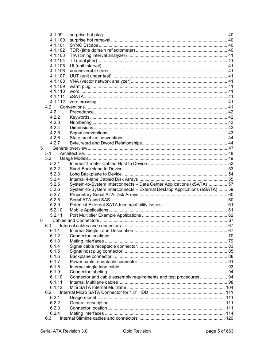
4.2 5.1 5.2 5 6 surprise hot plug .................................................................................................... 40 4.1.99 4.1.100 surprise hot removal .............................................................................................. 40 4.1.101 SYNC Escape........................................................................................................ 40 4.1.102 TDR (time domain reflectometer) .......................................................................... 40 4.1.103 TIA (timing interval analyzer)................................................................................. 41 4.1.104 TJ (total jitter)......................................................................................................... 41 4.1.105 UI (unit interval) ..................................................................................................... 41 4.1.106 unrecoverable error ............................................................................................... 41 4.1.107 UUT (unit under test) ............................................................................................. 41 4.1.108 VNA (vector network analyzer).............................................................................. 41 4.1.109 warm plug .............................................................................................................. 41 4.1.110 word ....................................................................................................................... 41 4.1.111 xSATA.................................................................................................................... 41 4.1.112 zero crossing ......................................................................................................... 41 Conventions................................................................................................................... 41 Precedence............................................................................................................ 42 4.2.1 Keywords ............................................................................................................... 42 4.2.2 4.2.3 Numbering ............................................................................................................. 43 4.2.4 Dimensions ............................................................................................................ 43 Signal conventions................................................................................................. 43 4.2.5 4.2.6 State machine conventions ................................................................................... 44 4.2.7 Byte, word and Dword Relationships..................................................................... 44 General overview..................................................................................................................47 Architecture.................................................................................................................... 48 Usage Models................................................................................................................ 49 Internal 1 meter Cabled Host to Device................................................................. 52 5.2.1 Short Backplane to Device .................................................................................... 53 5.2.2 Long Backplane to Device..................................................................................... 54 5.2.3 Internal 4-lane Cabled Disk Arrays........................................................................ 55 5.2.4 System-to-System Interconnects – Data Center Applications (xSATA)................ 57 5.2.5 System-to-System Interconnects – External Desktop Applications (eSATA)........ 59 5.2.6 Proprietary Serial ATA Disk Arrays ....................................................................... 60 5.2.7 5.2.8 Serial ATA and SAS .............................................................................................. 60 Potential External SATA Incompatibility Issues..................................................... 61 5.2.9 5.2.10 Mobile Applications................................................................................................ 61 5.2.11 Port Multiplier Example Applications ..................................................................... 62 Cables and Connectors ........................................................................................................67 Internal cables and connectors...................................................................................... 67 6.1.1 Internal Single Lane Description............................................................................ 67 Connector locations ............................................................................................... 70 6.1.2 Mating interfaces ................................................................................................... 79 6.1.3 Signal cable receptacle connector......................................................................... 83 6.1.4 6.1.5 Signal host plug connector .................................................................................... 85 6.1.6 Backplane connector ............................................................................................. 88 6.1.7 Power cable receptacle connector ........................................................................ 91 6.1.8 Internal single lane cable....................................................................................... 93 6.1.9 Connector labeling................................................................................................. 94 6.1.10 Connector and cable assembly requirements and test procedures ...................... 94 6.1.11 Internal Multilane cables........................................................................................ 98 6.1.12 Mini SATA Internal Multilane ............................................................................... 104 Internal Micro SATA Connector for 1.8” HDD ............................................................. 111 6.2.1 Usage model........................................................................................................ 111 General description.............................................................................................. 111 6.2.2 Connector location............................................................................................... 111 6.2.3 6.2.4 Mating interfaces ................................................................................................. 114 Internal Slimline cables and connectors...................................................................... 120 6.1 6.2 6.3 Serial ATA Revision 3.0 Gold Revision page 5 of 663
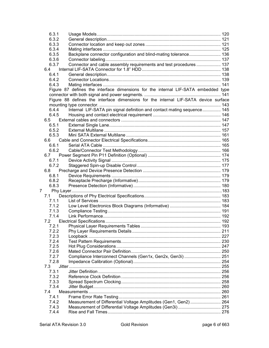
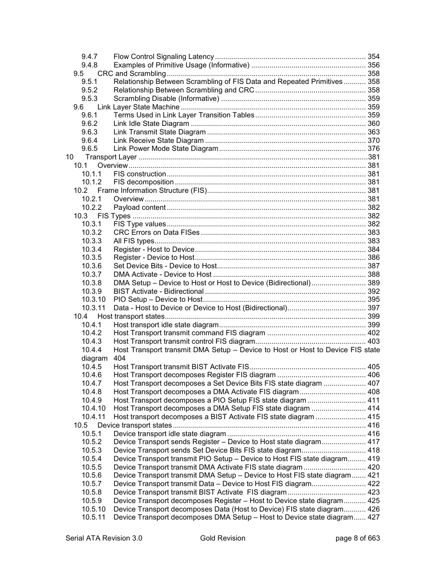
6.6 6.7 6.8 6.5 6.4 Usage Models...................................................................................................... 120 6.3.1 General description.............................................................................................. 121 6.3.2 Connector location and keep out zones .............................................................. 121 6.3.3 Mating interfaces ................................................................................................. 125 6.3.4 Backplane connector configuration and blind-mating tolerance.......................... 136 6.3.5 Connector labeling............................................................................................... 137 6.3.6 Connector and cable assembly requirements and test procedures .................... 137 6.3.7 Internal LIF-SATA Connector for 1.8” HDD................................................................. 138 General description.............................................................................................. 138 6.4.1 Connector Locations............................................................................................ 139 6.4.2 6.4.3 Mating interfaces ................................................................................................. 141 Figure 87 defines the interface dimensions for the internal LIF-SATA embedded type connector with both signal and power segments. ............................................................... 141 Figure 88 defines the interface dimensions for the internal LIF-SATA device surface mounting type connector. .................................................................................................... 143 6.4.4 Internal LIF-SATA pin signal definition and contact mating sequence............... 145 6.4.5 Housing and contact electrical requirement ........................................................ 146 External cables and connectors .................................................................................. 147 6.5.1 External Single Lane............................................................................................ 147 External Multilane ................................................................................................ 157 6.5.2 6.5.3 Mini SATA External Multilane .............................................................................. 161 Cable and Connector Electrical Specifications............................................................ 165 6.6.1 Serial ATA Cable ................................................................................................. 165 Cable/Connector Test Methodology.................................................................... 166 6.6.2 Power Segment Pin P11 Definition (Optional) ............................................................ 174 6.7.1 Device Activity Signal .......................................................................................... 175 Staggered Spin-up Disable Control ..................................................................... 177 6.7.2 Precharge and Device Presence Detection ................................................................ 179 Device Requirements .......................................................................................... 179 6.8.1 Receptacle Precharge (Informative).................................................................... 179 6.8.2 6.8.3 Presence Detection (Informative) ........................................................................ 180 Phy Layer............................................................................................................................183 Descriptions of Phy Electrical Specifications............................................................... 183 7.1.1 List of Services .................................................................................................... 183 Low Level Electronics Block Diagrams (Informative) .......................................... 184 7.1.2 7.1.3 Compliance Testing............................................................................................. 191 Link Performance................................................................................................. 192 7.1.4 Electrical Specifications............................................................................................... 192 7.2.1 Physical Layer Requirements Tables .................................................................. 193 Phy Layer Requirements Details ......................................................................... 211 7.2.2 Loopback ............................................................................................................. 227 7.2.3 Test Pattern Requirements.................................................................................. 230 7.2.4 7.2.5 Hot Plug Considerations...................................................................................... 247 7.2.6 Mated Connector Pair Definition.......................................................................... 250 7.2.7 Compliance Interconnect Channels (Gen1x, Gen2x, Gen3i) .............................. 251 Impedance Calibration (Optional)........................................................................ 254 7.2.8 Jitter ............................................................................................................................. 255 7.3.1 Jitter Definition ..................................................................................................... 256 Reference Clock Definition .................................................................................. 256 7.3.2 Spread Spectrum Clocking.................................................................................. 258 7.3.3 Jitter Budget......................................................................................................... 260 7.3.4 7.4 Measurements ............................................................................................................. 260 7.4.1 Frame Error Rate Testing.................................................................................... 261 Measurement of Differential Voltage Amplitudes (Gen1, Gen2) ......................... 264 7.4.2 7.4.3 Measurement of Differential Voltage Amplitudes (Gen3i) ................................... 275 7.4.4 Rise and Fall Times............................................................................................. 276 7.3 7 7.1 7.2 Serial ATA Revision 3.0 Gold Revision page 6 of 663
Transmitter Amplitude.......................................................................................... 278 7.4.5 Receive Amplitude............................................................................................... 279 7.4.6 Long Term Frequency Accuracy ......................................................................... 283 7.4.7 Jitter Measurements ............................................................................................ 284 7.4.8 Transmit Jitter (Gen1i, Gen2i, Gen1m, Gen2m, Gen1x, and Gen2x) ................. 287 7.4.9 Transmit Jitter (Gen3i) ......................................................................................... 289 7.4.10 7.4.11 Receiver Tolerance (Gen1i, Gen2i, Gen1m, Gen2m, Gen1x, and Gen2x)......... 290 7.4.12 Receiver Tolerance (Gen3i) ................................................................................ 292 7.4.13 Return Loss and Impedance Balance ................................................................. 294 7.4.14 SSC Profile .......................................................................................................... 298 7.4.15 Intra-Pair Skew .................................................................................................... 298 7.4.16 Sequencing Transient Voltage ............................................................................ 300 7.4.17 AC Coupling Capacitor ........................................................................................ 301 7.4.18 TX Amplitude Imbalance...................................................................................... 301 TX Rise/Fall Imbalance........................................................................................ 301 7.4.19 7.4.20 TX AC Common Mode Voltage (Gen2i, Gen2m) ................................................ 302 7.4.21 Tx AC Common Mode Voltage (Gen3i)............................................................... 302 7.4.22 OOB Common Mode Delta.................................................................................. 302 7.4.23 OOB Differential Delta ......................................................................................... 303 7.4.24 Squelch Detector Tests ....................................................................................... 303 7.4.25 OOB Signaling Tests ........................................................................................... 304 7.4.26 TDR Differential Impedance (Gen1i / Gen1m) .................................................... 305 7.4.27 TDR Single-Ended Impedance (Gen1i / Gen1m)................................................ 306 7.4.28 DC Coupled Common Mode Voltage (Gen1i / Gen1m) ...................................... 307 7.4.29 AC Coupled Common Mode Voltage (Gen1i / Gen1m) ...................................... 308 7.4.30 Sequencing Transient Voltage - Laboratory Load (Gen3i).................................. 309 Interface States............................................................................................................ 309 Out Of Band Signaling......................................................................................... 309 7.5.1 7.5.2 Idle Bus Condition................................................................................................ 317 Elasticity Buffer Management...................................................................................... 317 OOB and Phy Power States ...............................................................................................319 Interface Power States ................................................................................................ 319 Asynchronous Signal Recovery (Optional).................................................................. 319 Unsolicited COMINIT Usage (Informative) .......................................................... 319 OOB and Signature FIS return (Informative)............................................................... 320 Power-On Sequence State Machine ........................................................................... 320 Host Phy Initialization State Machine .................................................................. 320 8.4.1 8.4.2 Device Phy Initialization State Machine............................................................... 325 Speed Negotiation ............................................................................................... 329 8.4.3 Link Layer ...........................................................................................................................335 Overview...................................................................................................................... 335 9.1.1 Frame Transmission............................................................................................ 335 9.1.2 Frame Reception ................................................................................................. 335 Encoding Method......................................................................................................... 335 9.2.1 Notation and Conventions ................................................................................... 336 Character Code ................................................................................................... 337 9.2.2 9.2.3 Transmission Summary....................................................................................... 345 9.2.4 Reception Summary ............................................................................................ 346 Transmission Overview ............................................................................................... 348 Primitives ..................................................................................................................... 348 Overview.............................................................................................................. 348 Primitive Descriptions .......................................................................................... 349 Primitive Encoding ............................................................................................... 350 DMATP Primitive .................................................................................................. 351 CONTP Primitive .................................................................................................. 351 ALIGNP Primitive.................................................................................................. 354 9.4.1 9.4.2 9.4.3 9.4.4 9.4.5 9.4.6 8.2.1 9.1 9.2 9.3 9.4 7.5 7.6 8.1 8.2 8.3 8.4 8 9 Serial ATA Revision 3.0 Gold Revision page 7 of 663
9.6 10 9.5 Flow Control Signaling Latency ........................................................................... 354 9.4.7 Examples of Primitive Usage (Informative) ......................................................... 356 9.4.8 CRC and Scrambling................................................................................................... 358 Relationship Between Scrambling of FIS Data and Repeated Primitives ........... 358 9.5.1 Relationship Between Scrambling and CRC....................................................... 358 9.5.2 Scrambling Disable (Informative) ........................................................................ 359 9.5.3 Link Layer State Machine ............................................................................................ 359 Terms Used in Link Layer Transition Tables....................................................... 359 9.6.1 Link Idle State Diagram ....................................................................................... 360 9.6.2 Link Transmit State Diagram ............................................................................... 363 9.6.3 9.6.4 Link Receive State Diagram ................................................................................ 370 Link Power Mode State Diagram......................................................................... 376 9.6.5 Transport Layer ..................................................................................................................381 10.1 Overview...................................................................................................................... 381 FIS construction................................................................................................... 381 10.1.1 10.1.2 FIS decomposition ............................................................................................... 381 10.2 Frame Information Structure (FIS)............................................................................... 381 10.2.1 Overview.............................................................................................................. 381 10.2.2 Payload content ................................................................................................... 382 10.3 FIS Types .................................................................................................................... 382 10.3.1 FIS Type values................................................................................................... 382 10.3.2 CRC Errors on Data FISes .................................................................................. 383 10.3.3 All FIS types......................................................................................................... 383 10.3.4 Register - Host to Device..................................................................................... 384 10.3.5 Register - Device to Host..................................................................................... 386 10.3.6 Set Device Bits - Device to Host.......................................................................... 387 10.3.7 DMA Activate - Device to Host ............................................................................ 388 10.3.8 DMA Setup – Device to Host or Host to Device (Bidirectional)........................... 389 10.3.9 BIST Activate - Bidirectional ................................................................................ 392 10.3.10 PIO Setup – Device to Host................................................................................. 395 10.3.11 Data - Host to Device or Device to Host (Bidirectional)....................................... 397 10.4 Host transport states.................................................................................................... 399 10.4.1 Host transport idle state diagram......................................................................... 399 10.4.2 Host Transport transmit command FIS diagram ................................................. 402 10.4.3 Host Transport transmit control FIS diagram....................................................... 403 10.4.4 Host Transport transmit DMA Setup – Device to Host or Host to Device FIS state diagram 404 10.4.5 Host Transport transmit BIST Activate FIS.......................................................... 405 10.4.6 Host Transport decomposes Register FIS diagram ............................................ 406 10.4.7 Host Transport decomposes a Set Device Bits FIS state diagram ..................... 407 10.4.8 Host Transport decomposes a DMA Activate FIS diagram................................. 408 10.4.9 Host Transport decomposes a PIO Setup FIS state diagram ............................. 411 10.4.10 Host Transport decomposes a DMA Setup FIS state diagram ........................... 414 10.4.11 Host transport decomposes a BIST Activate FIS state diagram ......................... 415 10.5 Device transport states................................................................................................ 416 10.5.1 Device transport idle state diagram ..................................................................... 416 10.5.2 Device Transport sends Register – Device to Host state diagram...................... 417 10.5.3 Device Transport sends Set Device Bits FIS state diagram................................ 418 10.5.4 Device Transport transmit PIO Setup – Device to Host FIS state diagram......... 419 10.5.5 Device Transport transmit DMA Activate FIS state diagram............................... 420 10.5.6 Device Transport transmit DMA Setup – Device to Host FIS state diagram....... 421 10.5.7 Device Transport transmit Data – Device to Host FIS diagram........................... 422 10.5.8 Device Transport transmit BIST Activate FIS diagram....................................... 423 10.5.9 Device Transport decomposes Register – Host to Device state diagram........... 425 10.5.10 Device Transport decomposes Data (Host to Device) FIS state diagram........... 426 10.5.11 Device Transport decomposes DMA Setup – Host to Device state diagram...... 427 Serial ATA Revision 3.0 Gold Revision page 8 of 663
分享到:
收藏