www.ti.com
SLWS206D –FEBRUARY 2008 –REVISED NOVEMBER 2010
GC5322 Wideband Digital Predistortion Transmit Processor
Check for Samples: GC5322
GC5322
1FEATURES
2•
•
Integrated DUC, CFR, and DPD Solutions
40-MHz (28-Mhz) Signal Bandwidth, Third
(Fifth)-Order Expansion BW in DPD Section,
Maximum Complex Rate 140 Mhz
• DUC: up to 12 CDMA2000 or TD-SCDMA,
4 W-CDMA, 3–10 MHz or 1–20 MHz OFDMA
Carriers
• CFR: Typically Meets 3GPP TS 25.141 <6.5-dB
PAR, <8-dB PAR for OFDMA Signals
• DPD: Short-Term and Long-Term Memory
Compensation to 1 µs, Typical ACLR
Improvement > 20 dB
• Single-Antenna TX Mode, Single or Shared
Feedback
352-Ball S-PBGA Package, 27-mm × 27-mm
•
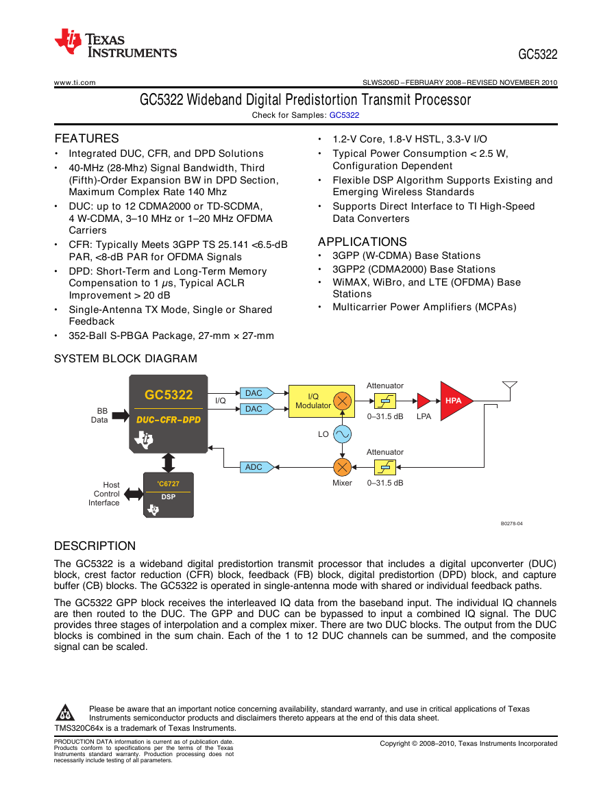
SYSTEM BLOCK DIAGRAM
1.2-V Core, 1.8-V HSTL, 3.3-V I/O
•
• Typical Power Consumption < 2.5 W,
Configuration Dependent
• Flexible DSP Algorithm Supports Existing and
Emerging Wireless Standards
• Supports Direct Interface to TI High-Speed
Data Converters
APPLICATIONS
•
•
• WiMAX, WiBro, and LTE (OFDMA) Base
3GPP (W-CDMA) Base Stations
3GPP2 (CDMA2000) Base Stations
Stations
• Multicarrier Power Amplifiers (MCPAs)
DESCRIPTION
The GC5322 is a wideband digital predistortion transmit processor that includes a digital upconverter (DUC)
block, crest factor reduction (CFR) block, feedback (FB) block, digital predistortion (DPD) block, and capture
buffer (CB) blocks. The GC5322 is operated in single-antenna mode with shared or individual feedback paths.
The GC5322 GPP block receives the interleaved IQ data from the baseband input. The individual IQ channels
are then routed to the DUC. The GPP and DUC can be bypassed to input a combined IQ signal. The DUC
provides three stages of interpolation and a complex mixer. There are two DUC blocks. The output from the DUC
blocks is combined in the sum chain. Each of the 1 to 12 DUC channels can be summed, and the composite
signal can be scaled.
1
Please be aware that an important notice concerning availability, standard warranty, and use in critical applications of Texas
Instruments semiconductor products and disclaimers thereto appears at the end of this data sheet.
2TMS320C64x is a trademark of Texas Instruments.
PRODUCTION DATA information is current as of publication date.
Products conform to specifications per the terms of
the Texas
Instruments standard warranty. Production processing does not
necessarily include testing of all parameters.
Copyright © 2008–2010, Texas Instruments Incorporated
GC5322DUC–CFR–DPDBBDataHostControlInterfaceDAC'C6727DSPDACI/QADCI/QModulatorLOMixerLPAHPAB0278-04Attenuator0–31.5 dBAttenuator0–31.5 dB�
GC5322
SLWS206D –FEBRUARY 2008 –REVISED NOVEMBER 2010
www.ti.com
These devices have limited built-in ESD protection. The leads should be shorted together or the device placed in conductive foam
during storage or handling to prevent electrostatic damage to the MOS gates.
DESCRIPTION (CONTINUED)
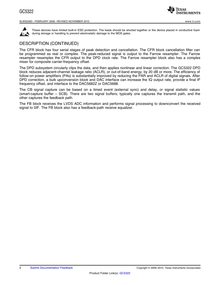
The CFR block has four serial stages of peak detection and cancellation. The CFR block cancellation filter can
be programmed as real or complex. The peak-reduced signal is output to the Farrow resampler. The Farrow
resampler resamples the CFR output to the DPD clock rate. The Farrow resampler block also has a complex
mixer for composite carrier-frequency offset.
The DPD subsystem circularly clips the data, and then applies nonlinear and linear correction. The GC5322 DPD
block reduces adjacent-channel leakage ratio (ACLR), or out-of-band energy, by 20 dB or more. The efficiency of
follow-on power amplifiers (PAs) is substantially improved by reducing the PAR and ACLR of digital signals. After
DPD correction, a bulk upconversion block and DAC interface can increase the IQ output rate, provide a final IF
frequency offset, and interface to the DAC5682Z or DAC5688.
The CB signal capture can be based on a timed event (external sync) and delay, or signal statistic values
(smart-capture buffer – SCB). There are two signal buffers; typically one captures the transmit path, and the
other captures the feedback path.
The FB block receives the LVDS ADC information and performs signal processing to downconvert the received
signal to 0IF. The FB block also has a feedback-path receive equalizer.
2
Submit Documentation Feedback
Copyright © 2008–2010, Texas Instruments Incorporated
Product Folder Link(s): GC5322
�
www.ti.com
SLWS206D –FEBRUARY 2008 –REVISED NOVEMBER 2010
GC5322 FUNCTIONAL BLOCK DIAGRAM
GC5322
TC
–40°C to 85°C
AVAILABLE OPTIONS
PACKAGED DEVICE(1)
352-ball S-PBGA package, 27 mm × 27 mm
GC5322IZND
(1) For the most current package and ordering information, see the Package Option Addendum at the end of this document, or see the TI
Web site at www.ti.com.
REFERENCES
1. GC5322_GC5325_architecture_datasheet_ext.pdf (obtain through local TI Field Application Engineer)
2. GC5325 System Evaluation Kit user's guide, schematic diagram (obtain through local TI Field Application
Engineer)
3. GC5322 configuration (TGTCFG) - (obtain through local TI Field Application Engineer)
4. DSP – TMS320C672x DSP Universal Host Port Interface Reference Guide (SPRU719)
5. DSP – TMS320C672x DSP External Memory Interface (EMIF) User's Guide (SPRU711)
Copyright © 2008–2010, Texas Instruments Incorporated
Submit Documentation Feedback
3
Product Folder Link(s): GC5322
BBinADCinADCclkDACout(LVDS)(LVDS)MAGoutMAGclkGainPilotInsertionAntCalInsertionPowerMeter161616238BBfrm1WideBandDUCWideBandDUCMediumBandDUCMediumBandDUCMediumBandDUCMediumBandDUCNarrowBand DUCNarrowBand DUCNarrowBand DUCNarrowBand DUCNarrowBand DUCNarrowBand DUCNarrowBand DUCNarrowBand DUCNarrowBand DUCNarrowBand DUCNarrowBand DUCNarrowBand DUC+CFRFractionalResamplerCircularLimiterGC5322JTAGMPU InterfaceResetBSync3SyncOutINTUPdataUPaddrOEBRDBWRBCEBTckTrstTITmsTO16164BBclkDPDclkBBPLLDPDPLLReal toComplexFeedbackEqualizerFeedback Mixerand NLCorrectionBulk Interpolation+ MixerTransmitEqualizerDPDADCInterfaceDACInterfaceEnvelopeInterfaceCapture BuffersDUCs in 1-Chn ModeDUCs in 2-Chn ModeDUCs in 6-Chn ModeBB Clock DomainDPD Clock DomainB0279-04�
GC5322
SLWS206D –FEBRUARY 2008 –REVISED NOVEMBER 2010
www.ti.com
DETAILED DESCRIPTION
GC5322 Introduction
The GC5322 is a flexible transmit sector processor that includes a digital upconverter (DUC) block, a crest factor
reduction (CFR) block, and a digital predistortion (DPD) block and its associated feedback chain. The GC5322
processes composite input bandwidths of up to 40 MHz and processes DPD expansion bandwidths of up to
140 MHz. By reducing the peak-to-average ratio (PAR) of the input signals using the CFR block and linearizing
the power amplifier (PA) using the DPD block, the GC5322 reduces the costs of multicarrier PAs (MCPA) for
wireless infrastructure applications. The GC5322 applies CFR and DPD, and a separate microprocessor (a
Texas Instruments TMS320C6727 DSP) is used to optimize performance levels and maintain target PA
performance levels.
By including the GC5322 in their system architecture, manufacturers of BTS equipment can realize significant
savings on power-amplifier bill of materials (BOM) and overall operational costs due to the PA efficiency
improvement. The GC5322 meets multicarrier 3G performance standards (PCDE, composite EVM, and ACLR) at
PAR levels down to 6.5 dB and improves the ACLR, at the PA output, by 20 dB or more. The GC5322 integrates
easily into the transmit signal chain between baseband processors (such as the Texas Instruments
TMS320C64x™ DSP family) and TI high-performance data converters.
A typical GC5322 system application includes the following transmit-chain components:
• TMS320C6727 digital signal processor (DSP)
• DAC5682 16-bit, 1-GSPS DAC; DAC5688 16-bit, 800-Msps DAC (transmit path)
• CDCM7005, CDCE72010 clock generator
• TRF3761 integrated VCO/PLL synthesizer
• TRF3703 quadrature modulator
• ADS5517 11-bit 200-MSPS ADC or ADS6149 14-bit, 250-MSPS ADC (feedback path)
• AMC7823 analog monitoring and control circuit with GPIO and SPI
4
Submit Documentation Feedback
Copyright © 2008–2010, Texas Instruments Incorporated
Product Folder Link(s): GC5322
�
www.ti.com
SLWS206D –FEBRUARY 2008 –REVISED NOVEMBER 2010
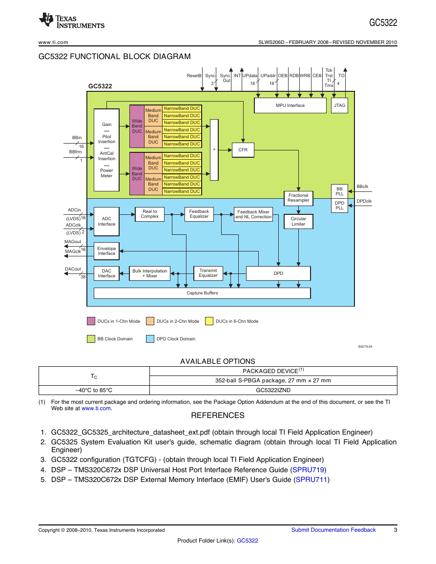
GC5322 SYSTEM ARCHITECTURE
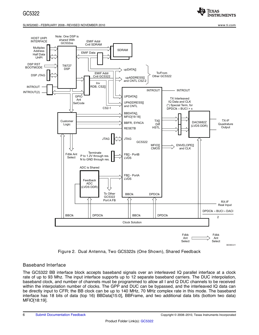
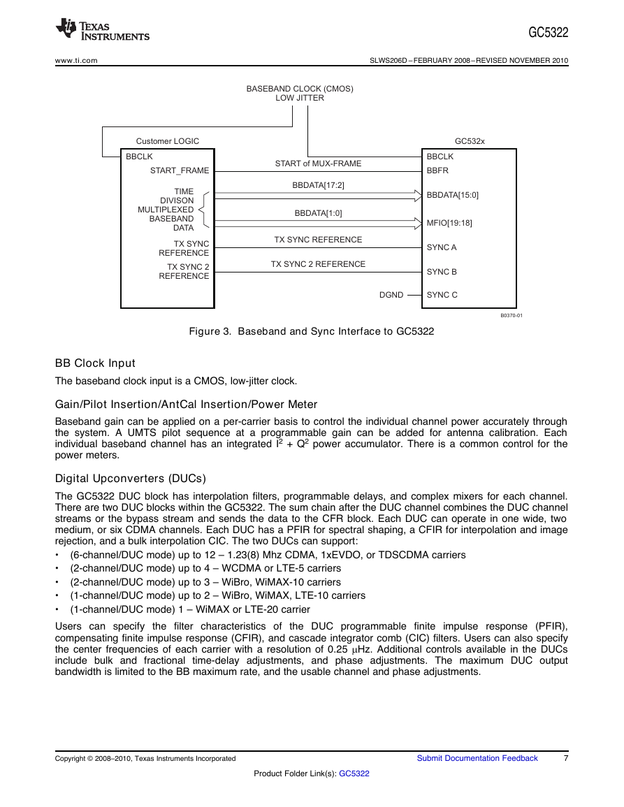
The GC5322 system architecture can be modified to suit a number of different antenna streams. There is a
tradeoff between the number of antenna streams per GC5322, and shared ADC feedback. Figure 1 shows a
single-antenna configuration, where one GC5322 is used. There are several other architectures possible:
Architecture
Figure
Benefit
Tradeoff/Complexity
GC5322
One antenna stream, up to
140-MHz DPD bandwidth,
added envelope output
(fifth-order correction, 28-Mhz
BW)
Two antenna streams, up to
140-MHz DPD bandwidth,
shared feedback ADC
(fifth-order correction, 28-Mhz
BW)
Figure 1
Figure 2
Magnitude output for power
amplifier drain modulator can
increase efficiency
Reduced cost of feedback
path DSP shared between
two GC5322s; GC5325 EVM to select CS2-CEB(2). Slower adaptation
as example
DSP must output antenna-select value using
HD22.20. Antenna-select value is also used
time
Figure 1. Single-Antenna GC5322 System Diagram (Envelope Output Added)
Copyright © 2008–2010, Texas Instruments Incorporated
Submit Documentation Feedback
5
Product Folder Link(s): GC5322
TX InterleavedIQ Data and CLK(*) SpecialTerm, forDPDClkBUCI > x´FeedbackADC(LVDS DDR)TX[]DiffHSTLFB[] - PortALVDSFB[] - PortBLVDSTerminatePto 1.2V through res.N to GND through res.GC5322TI6727DSPJTAGDSPJTAGJTAGDSPRSTBOOTMODEMultiplexAddressHalf DataUHPIEMIFAddrCntl SDRAMEMIF DataEMIFAddrCntl GC5322RESETBBBDATA[],MFIO[19:18]BBFR, SYNCAENVELOPE[]and CLKMFIO[]CMOSINTROUTINTROUTINTROUTClock SolutionBBClkBBClkBBClkDPDClkDPDClkDPDClkInvRDBHOSTUHPIINTERFACEUPDATA[]UPADDRESS[]and CNTLCustomerLogicB0379-01SDRAMresDAC5682Z(LVDS DDR)TX-IFQuadratureOutputRX-IFReal InputDPDClkBUCIDACI2´´�
GC5322
SLWS206D –FEBRUARY 2008 –REVISED NOVEMBER 2010
www.ti.com
Figure 2. Dual Antenna, Two GC5322s (One Shown), Shared Feedback
Baseband Interface
The GC5322 BB interface block accepts baseband signals over an interleaved IQ parallel interface at a clock
rate of up to 93 Mhz. The input interface supports up to 12 separate baseband carriers. The DUC interpolation,
baseband clock, and number of channels must be programmed to allow all I and Q DUC channels to be received
within the interpolation number of clocks. The GPP and DUC can be bypassed, and the interleaved IQ data can
be directly input to CFR; the BB clock can be up to 140 MHz, 70 MHz complex rate in this mode. The baseband
interface has 18 bits of data (top 16) BBData[15:0], BBFrame, and two additional data bits (bottom two data)
MFIO[18:19].
6
Submit Documentation Feedback
Copyright © 2008–2010, Texas Instruments Incorporated
Product Folder Link(s): GC5322
TX InterleavedIQ Data and CLK(*) SpecialTerm, forDPDClkBUCI > x´FeedbackADC(LVDS DDR)TX[]DiffHSTLFB[] - PortALVDSFB[] - PortBLVDSTerminatePto 1.2V through res.N to GND through res.GC5322JTAGDSPJTAGJTAGDSPRSTBOOTMODEMultiplexAddressHalf DataUHPIEMIFAddrCntl SDRAMEMIF DataupDATA[]upADDRESS[]and CNTLCS2-2EMIFAddrCntl GC5322RESETBBBDATA[],MFIO[19:18]BBFR, SYNCAENVELOPE[]and CLKMFIO[]CMOSINTROUTINTROUTINTROUTClock SolutionBBClkBBClkBBClkDPDClkDPDClkDPDClkInvRDB, CS2[]HOSTUHPIINTERFACETo/FromOther GC5322UPDATA[]UPADDRESS[]and CNTLGPIOAntSelCodeFdbkAntSelectFdbkAntSelectFdbkAntSelectINTROUT(2)CS2-1ADC is SharedTo OtherGC5322PortAFBCustomerLogicresB0380-01Note: One DSPisshared WithGC532xsTI6727DSPSDRAMDAC5682Z(LVDS DDR)TX-IFQuadratureOutputRX-IFReal InputDPDClkBUCIDACI2´´�
www.ti.com
SLWS206D –FEBRUARY 2008 –REVISED NOVEMBER 2010
GC5322
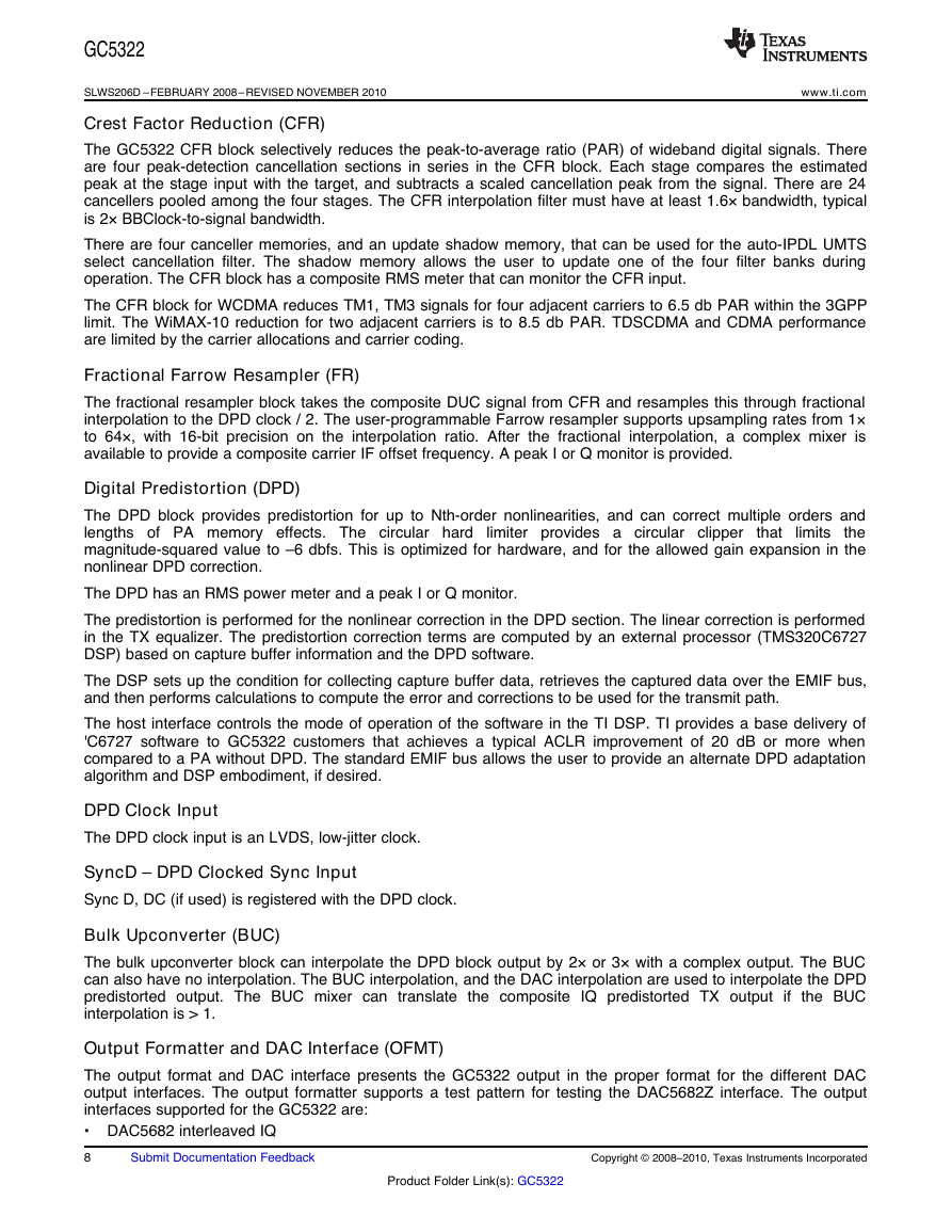
Figure 3. Baseband and Sync Interface to GC5322
BB Clock Input
The baseband clock input is a CMOS, low-jitter clock.
Gain/Pilot Insertion/AntCal Insertion/Power Meter
Baseband gain can be applied on a per-carrier basis to control the individual channel power accurately through
the system. A UMTS pilot sequence at a programmable gain can be added for antenna calibration. Each
individual baseband channel has an integrated I2 + Q2 power accumulator. There is a common control for the
power meters.
Digital Upconverters (DUCs)
The GC5322 DUC block has interpolation filters, programmable delays, and complex mixers for each channel.
There are two DUC blocks within the GC5322. The sum chain after the DUC channel combines the DUC channel
streams or the bypass stream and sends the data to the CFR block. Each DUC can operate in one wide, two
medium, or six CDMA channels. Each DUC has a PFIR for spectral shaping, a CFIR for interpolation and image
rejection, and a bulk interpolation CIC. The two DUCs can support:
•
•
•
•
•
Users can specify the filter characteristics of
the DUC programmable finite impulse response (PFIR),
compensating finite impulse response (CFIR), and cascade integrator comb (CIC) filters. Users can also specify
the center frequencies of each carrier with a resolution of 0.25 mHz. Additional controls available in the DUCs
include bulk and fractional
time-delay adjustments, and phase adjustments. The maximum DUC output
bandwidth is limited to the BB maximum rate, and the usable channel and phase adjustments.
(6-channel/DUC mode) up to 12 – 1.23(8) Mhz CDMA, 1xEVDO, or TDSCDMA carriers
(2-channel/DUC mode) up to 4 – WCDMA or LTE-5 carriers
(2-channel/DUC mode) up to 3 – WiBro, WiMAX-10 carriers
(1-channel/DUC mode) up to 2 – WiBro, WiMAX, LTE-10 carriers
(1-channel/DUC mode) 1 – WiMAX or LTE-20 carrier
Copyright © 2008–2010, Texas Instruments Incorporated
Submit Documentation Feedback
7
Product Folder Link(s): GC5322
GC532xBBFRTX SYNC REFERENCEDGNDSYNCASYNCBSYNCCCustomer LOGICBBDATA[17:2]B0370-01BBCLKSTART_FRAMETIMEDIVISONMULTIPLEXEDBASEBANDDATATX SYNCREFERENCETX SYNC 2REFERENCEBASEBAND CLOCK (CMOS)LOW JITTERBBCLKSTARTof MUX-FRAMEBBDATA[1:0]TX SYNC 2 REFERENCEBBDATA[15:0]MFIO[19:18]�
GC5322
SLWS206D –FEBRUARY 2008 –REVISED NOVEMBER 2010
www.ti.com
Crest Factor Reduction (CFR)
The GC5322 CFR block selectively reduces the peak-to-average ratio (PAR) of wideband digital signals. There
are four peak-detection cancellation sections in series in the CFR block. Each stage compares the estimated
peak at the stage input with the target, and subtracts a scaled cancellation peak from the signal. There are 24
cancellers pooled among the four stages. The CFR interpolation filter must have at least 1.6× bandwidth, typical
is 2× BBClock-to-signal bandwidth.
There are four canceller memories, and an update shadow memory, that can be used for the auto-IPDL UMTS
select cancellation filter. The shadow memory allows the user to update one of the four filter banks during
operation. The CFR block has a composite RMS meter that can monitor the CFR input.
The CFR block for WCDMA reduces TM1, TM3 signals for four adjacent carriers to 6.5 db PAR within the 3GPP
limit. The WiMAX-10 reduction for two adjacent carriers is to 8.5 db PAR. TDSCDMA and CDMA performance
are limited by the carrier allocations and carrier coding.
Fractional Farrow Resampler (FR)
The fractional resampler block takes the composite DUC signal from CFR and resamples this through fractional
interpolation to the DPD clock / 2. The user-programmable Farrow resampler supports upsampling rates from 1×
to 64×, with 16-bit precision on the interpolation ratio. After the fractional
interpolation, a complex mixer is
available to provide a composite carrier IF offset frequency. A peak I or Q monitor is provided.
Digital Predistortion (DPD)
The DPD block provides predistortion for up to Nth-order nonlinearities, and can correct multiple orders and
lengths of PA memory effects. The circular hard limiter provides a circular clipper
limits the
magnitude-squared value to –6 dbfs. This is optimized for hardware, and for the allowed gain expansion in the
nonlinear DPD correction.
The DPD has an RMS power meter and a peak I or Q monitor.
The predistortion is performed for the nonlinear correction in the DPD section. The linear correction is performed
in the TX equalizer. The predistortion correction terms are computed by an external processor (TMS320C6727
DSP) based on capture buffer information and the DPD software.
The DSP sets up the condition for collecting capture buffer data, retrieves the captured data over the EMIF bus,
and then performs calculations to compute the error and corrections to be used for the transmit path.
The host interface controls the mode of operation of the software in the TI DSP. TI provides a base delivery of
'C6727 software to GC5322 customers that achieves a typical ACLR improvement of 20 dB or more when
compared to a PA without DPD. The standard EMIF bus allows the user to provide an alternate DPD adaptation
algorithm and DSP embodiment, if desired.
that
DPD Clock Input
The DPD clock input is an LVDS, low-jitter clock.
SyncD – DPD Clocked Sync Input
Sync D, DC (if used) is registered with the DPD clock.
Bulk Upconverter (BUC)
The bulk upconverter block can interpolate the DPD block output by 2× or 3× with a complex output. The BUC
can also have no interpolation. The BUC interpolation, and the DAC interpolation are used to interpolate the DPD
predistorted output. The BUC mixer can translate the composite IQ predistorted TX output
the BUC
interpolation is > 1.
if
Output Formatter and DAC Interface (OFMT)
The output format and DAC interface presents the GC5322 output in the proper format for the different DAC
output interfaces. The output formatter supports a test pattern for testing the DAC5682Z interface. The output
interfaces supported for the GC5322 are:
• DAC5682 interleaved IQ
8
Submit Documentation Feedback
Copyright © 2008–2010, Texas Instruments Incorporated
Product Folder Link(s): GC5322
�



 2023年江西萍乡中考道德与法治真题及答案.doc
 2012年重庆南川中考生物真题及答案.doc
 2013年江西师范大学地理学综合及文艺理论基础考研真题.doc
 2020年四川甘孜小升初语文真题及答案I卷.doc
 2020年注册岩土工程师专业基础考试真题及答案.doc
 2023-2024学年福建省厦门市九年级上学期数学月考试题及答案.doc
 2021-2022学年辽宁省沈阳市大东区九年级上学期语文期末试题及答案.doc
 2022-2023学年北京东城区初三第一学期物理期末试卷及答案.doc
 2018上半年江西教师资格初中地理学科知识与教学能力真题及答案.doc
 2012年河北国家公务员申论考试真题及答案-省级.doc
 2020-2021学年江苏省扬州市江都区邵樊片九年级上学期数学第一次质量检测试题及答案.doc
 2022下半年黑龙江教师资格证中学综合素质真题及答案.doc