CHC2442 Application Note
Date: 15 March, 2017
�
Purpose of document
This document provides guide lines for use of CHC2442
Hardware configuration required :
UMS Demo Board PCB n°502256A or customer PCB
Optional:
Board USB-SPI MCP2210
Mini USB/USB cable
Connection cables (DC and RF – not provided)
USB key with dedicated software
Software configuration required:
Windows OS PC
MCP2210_SpiTerminal-v1.0.zip to be installed for USB-SPI control
Excel sheet CHC2442 SPI settings.xlsx for CHC2442 SPI register settings
and definitions
Documentation
CHC2442 Datasheet
3-Jan-17 / CHC2442 application note
2
All information contained in this document remains the sole and exclusive property of UNITED MONOLITHIC SEMICONDUCTORS SAS and shall not
be disclosed by the recipient to third party without the prior consent of UNITED MONOLITHIC SEMICONDUCTORS SAS.
�
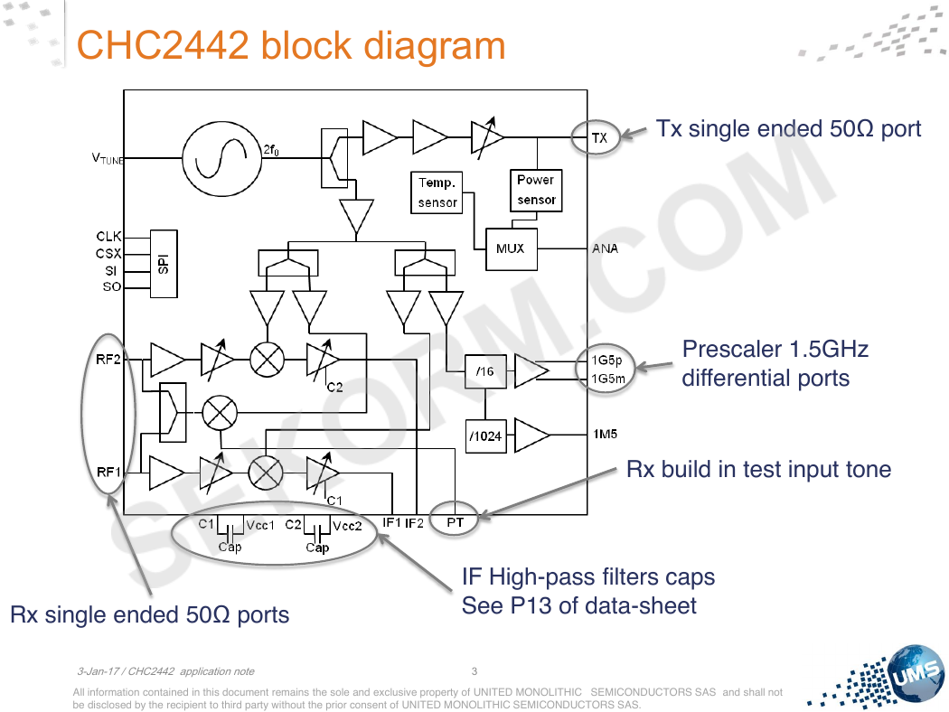
CHC2442 block diagram
Tx single ended 50Ω port
Prescaler 1.5GHz
differential ports
Rx build in test input tone
Rx single ended 50Ω ports
IF High-pass filters caps
See P13 of data-sheet
3-Jan-17 / CHC2442 application note
3
All information contained in this document remains the sole and exclusive property of UNITED MONOLITHIC SEMICONDUCTORS SAS and shall not
be disclosed by the recipient to third party without the prior consent of UNITED MONOLITHIC SEMICONDUCTORS SAS.
�
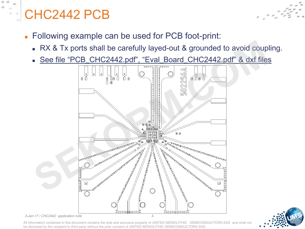
CHC2442 PCB
Following example can be used for PCB foot-print:
RX & Tx ports shall be carefully layed-out & grounded to avoid coupling.
See file “PCB_CHC2442.pdf”, “Eval_Board_CHC2442.pdf” & dxf files
3-Jan-17 / CHC2442 application note
4
All information contained in this document remains the sole and exclusive property of UNITED MONOLITHIC SEMICONDUCTORS SAS and shall not
be disclosed by the recipient to third party without the prior consent of UNITED MONOLITHIC SEMICONDUCTORS SAS.
�
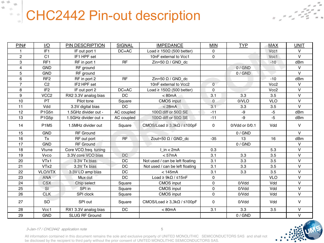
CHC2442 Pin-out description
IMPEDANCE
MIN
TYP
I/O
IF1
C1
RF1
GND
GND
RF2
C2
IF2
PIN DESCRIPTION
IF out port 1
IF1 HPF set
RF in port 1
RF ground
RF ground
RF in port 2
IF2 HPF set
IF out port 2
VCC2
RX2 3.3V analog bias
Pilot tone
3.3V digital bias
SIGNAL
DC+AC
RF
RF
DC+AC
DC
Square
DC
Load ≥ 150Ω (500 better)
10nF external to Vcc1
Zin=50 Ω / GND_dc
Zin=50 Ω / GND_dc
10nF external to Vcc2
Load ≥ 150Ω (500 better)
< 80mA
CMOS input
< 28mA
3-Jan-17 / CHC2442 application note
All information contained in this document remains the sole and exclusive property of UNITED MONOLITHIC SEMICONDUCTORS SAS and shall not
be disclosed by the recipient to third party without the prior consent of UNITED MONOLITHIC SEMICONDUCTORS SAS.
PIN#
1
2
3
4
5
6
7
8
9
10
11
12
13
14
15
16
17
18
19
20
21
22
23
24
25
26
27
28
29
PT
Vdd
P1G5n
P1G5p
P1M5
GND
Tx
GND
Vtune
Vvco
VTx1
VTx2
ANA
CSX
SI
CLK
SO
Vcc1
GND
VLO/VTX
3.3V LO amp bias
1.5GHz divider out -
1.5GHz divider out +
AC coupled
AC coupled
100Ω diff or 50Ω SE
100Ω diff or 50Ω SE
1.5MHz divider out
Square
CMOS/Load ≥ 3,3kΩ / ≤100pF
RF Ground
RF out port
RF Ground
Core VCO freq. tuning
3.3V core VCO bias
3.3V Tx bias
3.3V Tx bias
Mux out
Chip select
SPI in
SPI clock
RF
DC
DC
DC
DC
DC
Square
Square
Square
Zout=50 Ω / GND_dc
I_in < 2mA
< 57mA
Not used / can be left floating
Not used / can be left floating
< 145mA
Load ≥ 9kΩ / ≤15nF
CMOS input
CMOS input
CMOS input
SPI out
Square
CMOS/Load ≥ 3,3kΩ / ≤100pF
RX1 3.3V analog bias
SLUG RF Ground
DC
< 80mA
5
0
0
0
0
3.1
0
3.1
-11
-11
0
-35
0.3
3.1
3.1
3.1
3.1
0
0
0
0
0
3.1
0 / GND
0 / GND
3.3
0/VLO
3.3
-9
-9
0/Vdd or 0/0.1
0 / GND
13
0 / GND
3.3
3.3
3.3
3.3
0/Vdd
0/Vdd
0/Vdd
0/Vdd
3.3
0 / GND
MAX
Vcc1
Vcc1
-10
-10
Vcc2
Vcc2
3.5
VLO
3.5
-5
-5
Vdd
16
5.3
3.5
3.5
3.5
3.5
VLO
Vdd
Vdd
Vdd
Vdd
3.5
UNIT
V
V
dBm
V
V
dBm
V
V
V
V
V
dBm
dBm
V
V
dBm
V
V
V
V
V
V
V
V
V
V
V
V
V
�
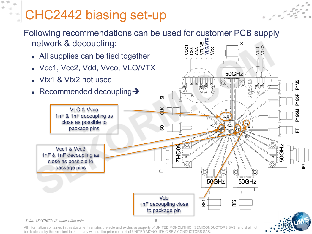
Following recommendations can be used for customer PCB supply
/
X
T
V
O
L
V
CHC2442 biasing set-up
network & decoupling:
All supplies can be tied together
Vcc1, Vcc2, Vdd, Vvco, VLO/VTX
Vtx1 & Vtx2 not used
Recommended decoupling
VLO & Vvco
1nF & 1nF decoupling as
close as possible to
package pins
Vcc1 & Vcc2
1nF & 1nF decoupling as
close as possible to
package pins
Vdd
1nF decoupling close
to package pin
3-Jan-17 / CHC2442 application note
6
All information contained in this document remains the sole and exclusive property of UNITED MONOLITHIC SEMICONDUCTORS SAS and shall not
be disclosed by the recipient to third party without the prior consent of UNITED MONOLITHIC SEMICONDUCTORS SAS.
�
CHC2442 Ports tips (continued)
Prescaler 1.5GHz ports:
Unused 1G5 output shall be left floating.
When loaded to single ended (like 50Ω to GND), it shall be AC coupled with
serial cap ≈1nF, to avoid DC current flow.
Can be used differential without serial caps.
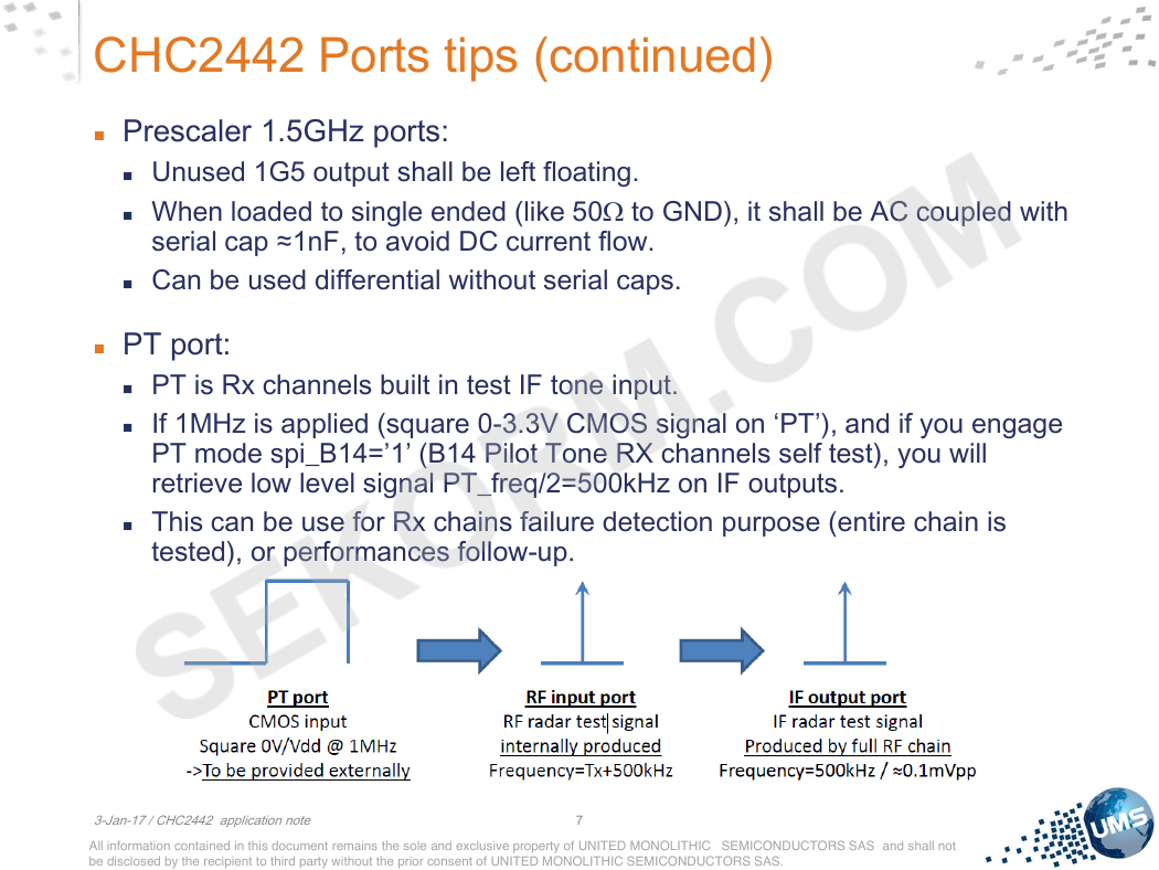
PT port:
PT is Rx channels built in test IF tone input.
If 1MHz is applied (square 0-3.3V CMOS signal on ‘PT’), and if you engage
PT mode spi_B14=’1’ (B14 Pilot Tone RX channels self test), you will
retrieve low level signal PT_freq/2=500kHz on IF outputs.
This can be use for Rx chains failure detection purpose (entire chain is
tested), or performances follow-up.
3-Jan-17 / CHC2442 application note
7
All information contained in this document remains the sole and exclusive property of UNITED MONOLITHIC SEMICONDUCTORS SAS and shall not
be disclosed by the recipient to third party without the prior consent of UNITED MONOLITHIC SEMICONDUCTORS SAS.
�
CHC2442 Ports tips (continued)
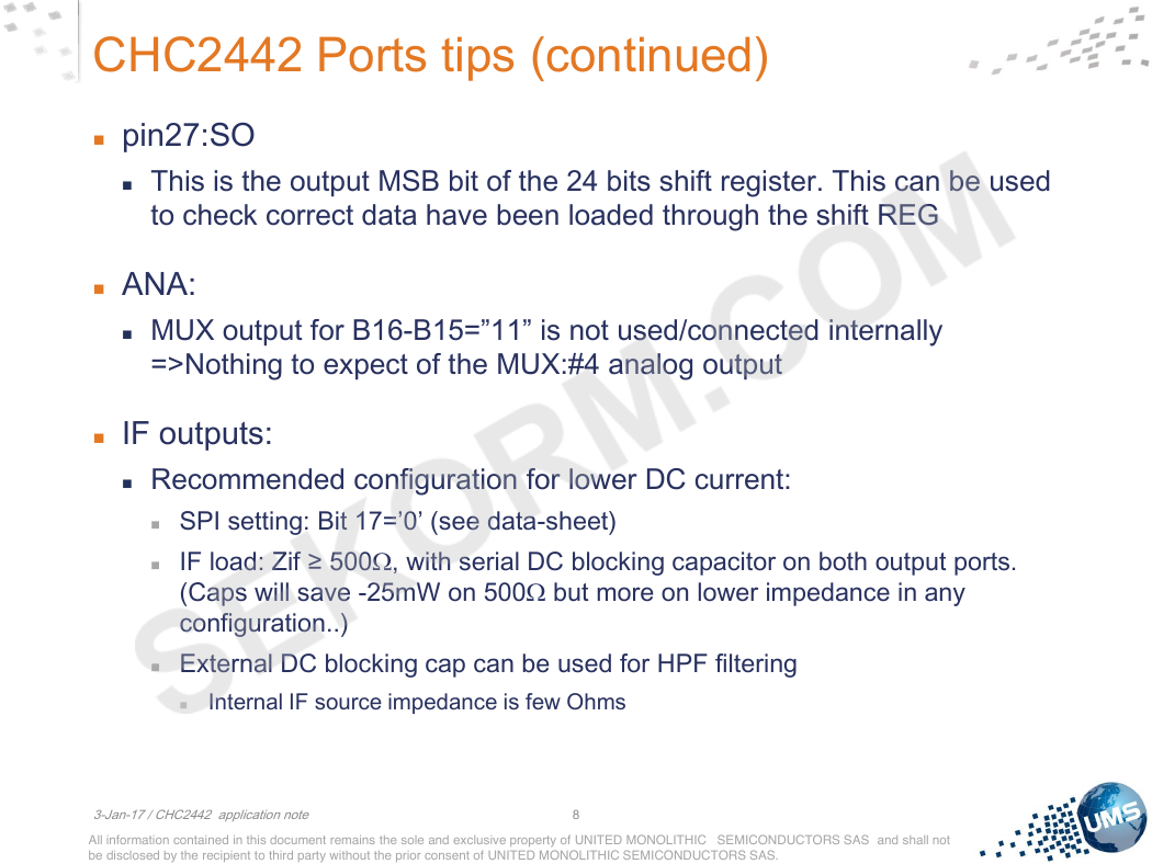
pin27:SO
This is the output MSB bit of the 24 bits shift register. This can be used
to check correct data have been loaded through the shift REG
ANA:
MUX output for B16-B15=”11” is not used/connected internally
=>Nothing to expect of the MUX:#4 analog output
IF outputs:
Recommended configuration for lower DC current:
SPI setting: Bit 17=’0’ (see data-sheet)
IF load: Zif ≥ 500Ω, with serial DC blocking capacitor on both output ports.
(Caps will save -25mW on 500Ω but more on lower impedance in any
configuration..)
External DC blocking cap can be used for HPF filtering
Internal IF source impedance is few Ohms
3-Jan-17 / CHC2442 application note
8
All information contained in this document remains the sole and exclusive property of UNITED MONOLITHIC SEMICONDUCTORS SAS and shall not
be disclosed by the recipient to third party without the prior consent of UNITED MONOLITHIC SEMICONDUCTORS SAS.
�




 2023年江西萍乡中考道德与法治真题及答案.doc
 2012年重庆南川中考生物真题及答案.doc
 2013年江西师范大学地理学综合及文艺理论基础考研真题.doc
 2020年四川甘孜小升初语文真题及答案I卷.doc
 2020年注册岩土工程师专业基础考试真题及答案.doc
 2023-2024学年福建省厦门市九年级上学期数学月考试题及答案.doc
 2021-2022学年辽宁省沈阳市大东区九年级上学期语文期末试题及答案.doc
 2022-2023学年北京东城区初三第一学期物理期末试卷及答案.doc
 2018上半年江西教师资格初中地理学科知识与教学能力真题及答案.doc
 2012年河北国家公务员申论考试真题及答案-省级.doc
 2020-2021学年江苏省扬州市江都区邵樊片九年级上学期数学第一次质量检测试题及答案.doc
 2022下半年黑龙江教师资格证中学综合素质真题及答案.doc