Application Report
SBOA122–November 2009
Transimpedance Considerations for High-Speed
Amplifiers
Xavier Ramus .................................................................................................... High-Speed Products
Designing high-resolution detection circuits using photodiodes presents considerable challenges because
bandwidth, gain, and input-referred noise are coupled together. This application note reviews the basic
issues of transimpedance design, provides a set of detailed design equations, explains those equations,
and develops an approach to easily compare potential solutions.
ABSTRACT
Contents
Introduction .................................................................................................................. 2
Stability Analysis ............................................................................................................ 2
Bandwidth Considerations ................................................................................................. 5
Noise Considerations ....................................................................................................... 6
Example ...................................................................................................................... 7
DC-Parameters Consideration ............................................................................................ 8
Conclusion ................................................................................................................... 8
List of Figures
Transimpedance Circuit with Modeled Elements ....................................................................... 2
Bode Plot Magnitude ....................................................................................................... 3
Maximum Achievable Bandwidth for Selected Op Amps (10pF Source Capacitance) ............................ 5
Noise Analysis Circuit ...................................................................................................... 6
310kΩ Transimpedance Gain with 200pF Source Capacitance Circuit.............................................. 8
Maximum Achievable Bandwidth vs Transimpedance Gain for Selected Op Amps ............................... 8
1
2
3
4
5
6
7
1
2
3
4
5
6
All trademarks are the property of their respective owners.
SBOA122– November 2009
Submit Documentation Feedback
Transimpedance Considerations for High-Speed Amplifiers
1
Copyright © 2009, Texas Instruments Incorporated
�
Introduction
www.ti.com
1
Introduction
The purpose of a transimpedance circuit is to convert an input current from a current source (typically a
photodiode) into an output voltage. The simplest method to achieve this conversion is to use a resistor
connected to ground. However, the achievable gain using this method is limited by the following factors:
1. The current source input impedance;
2. The load impedance; and
3. Desired bandwidth.
A closed-loop approach, using an operational amplifier, is normally beneficial to most applications as it
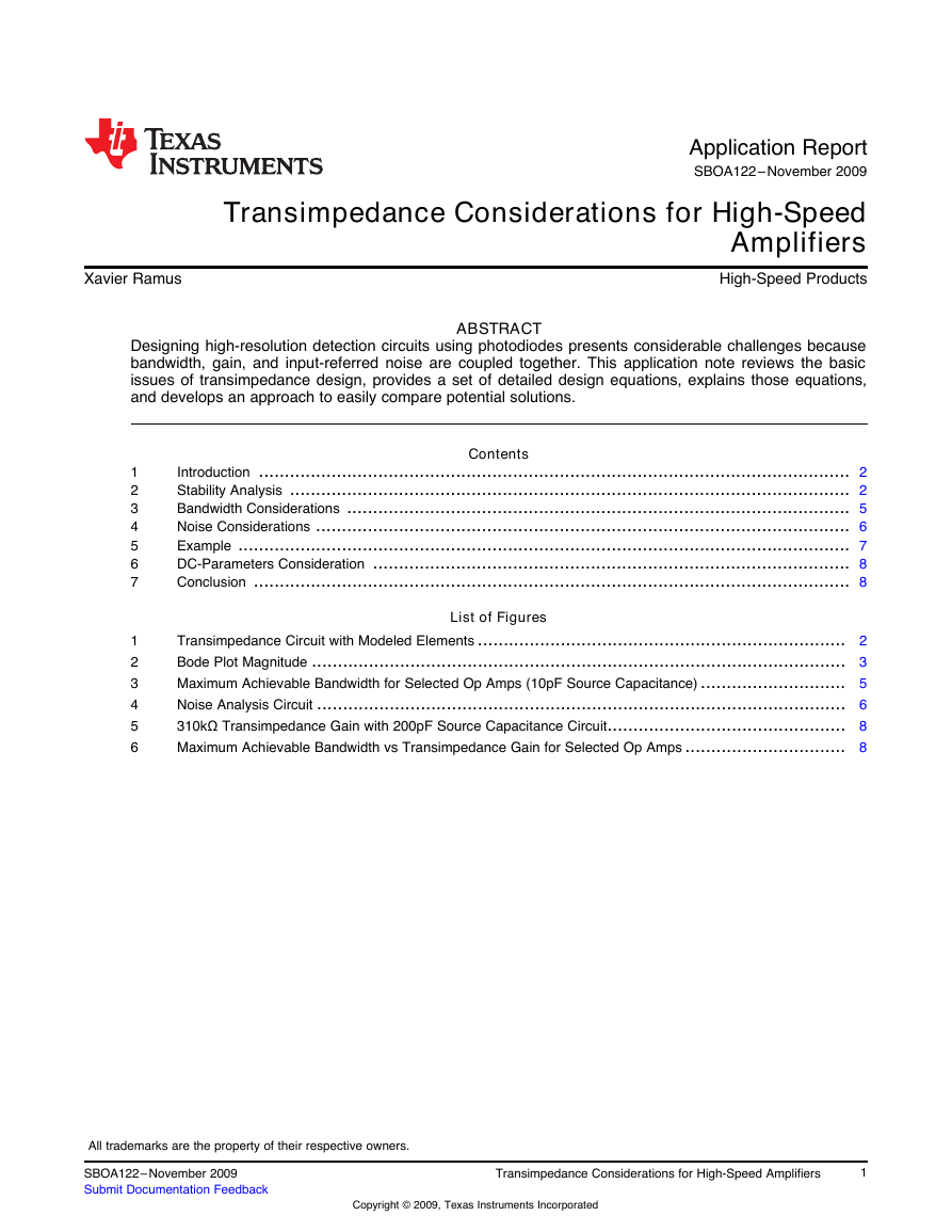
has the potential of eliminating those issues. A typical circuit with all necessary components for this
analysis is shown in Figure 1. In this circuit, the generator is a photodiode, whose role is to convert the
photons into a current. This current is then amplified by the feedback resistor RF. Working with an ideal
amplifier for now, we can see that because no bias current is present, all the signal generated by the
photodiode is going to be converted to the output. Note that the source impedance is not of interest here;
it is isolated from the output. Note also that the output is low impedance, allowing a wide variety of load to
be connected. The bandwidth is going to be a function of the source capacitance (CS), the feedback
capacitance (CF), and the gain bandwidth product of the actual amplifier used.
Figure 1. Transimpedance Circuit with Modeled Elements
The source capacitance (CS) is the sum of the photodiode capacitance (CD), the common-mode
capacitance of the amplifier (CCM), and the differential capacitance of the amplifier (CDIFF). CCM and CDIFF
include both the board layout and the op amp parasitic capacitance.
2
Stability Analysis
The first non-ideal op-amp characteristic we examine here is the non-infinite open-loop gain. The
architecture for the operational amplifier used in the rest of this application report is a single pole op-amp
model, as shown in Equation 1. This model allows us to analyze the resulting transimpedance design as a
second-order, closed-loop transfer function.
Expressing the Laplace transfer function in Bode analysis form yields the following equation.
(1)
(2)
2
Transimpedance Considerations for High-Speed Amplifiers
SBOA122– November 2009
Submit Documentation Feedback
Copyright © 2009, Texas Instruments Incorporated
-VBlA(s)VOCFCCMCDCDIFFRFIDV-C= C+ C+ CSDCMDIFFV=VA(s)O--A(s) =As +wwOLAA·VIOD=-ZF1 +1 +ZZFGA(s)�
www.ti.com
where:
Stability Analysis
(3)
(4)
At dc, and if the open-loop gain of the amplifier is infinite, the amplifier gain is set by the feedback resistor.
This effect can be seen by setting s = 0 in Equation 3 and plugging the result into Equation 2 while setting
A(s) = ∞.
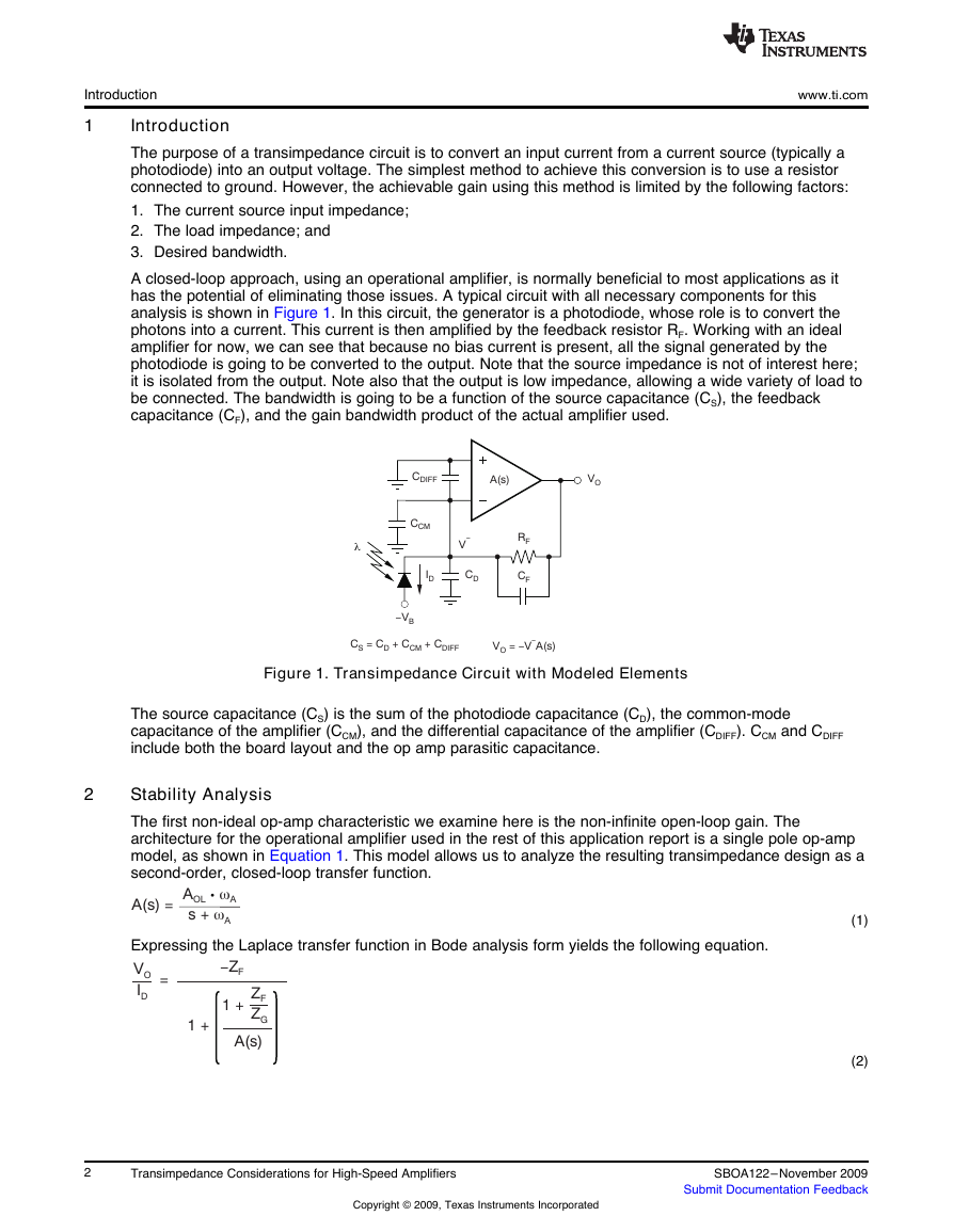
is the noise gain. The loop gain is the difference between the open-loop gain (AOL) and the noise
gain. The noise gain is plotted in Figure 2 alongside the single pole, open-loop gain model of the amplifier.
Figure 2. Bode Plot Magnitude
At dc, the gain is indeed the expected transimpedance gain RF, while at high frequency, it is
. Note
that only the feedback capacitor (CF) and the source capacitance (CS) are used for stability; consequently,
it can be noted that a unity-gain stable amplifier is not necessary for transimpedance applications. In fact,
it is recommended to use a decompensated amplifier instead, because these decompensated amplifiers
offer better voltage noise specifications and larger gain bandwidth products than any compensated
version. This fact is easily illustrated by two families of devices: the OPA842/3/6/7 and the OPA656/7. The
OPA842 is unity-gain stable and has 2.7nV/√Hz input voltage noise. The OPA843 is stable for gains
greater than 3V/V and has a voltage noise of 2nV/√Hz. The OPA846 is stable for gains greater than 7V/V
and has a 1.2nV/√Hz voltage noise. Finally, the OPA847 has a voltage noise of 0.85nV/√Hz and is stable
for gains greater than 12V/V. For FET devices such as the OPA656 and OPA657, the OPA656 provides
unity-gain stability with a 7nV/√Hz input voltage noise; the OPA657 has a 4.8nV/√Hz voltage noise, but is
stable for gains greater than 7V/V.
Coming back to the analysis and expressing the full transfer function as a function of ωo and Q.—given in
Equation 5 with Equation 6 and Equation 7 expressing ωo and Q with physical elements of the circuit
—yields the following results:
SBOA122– November 2009
Submit Documentation Feedback
Transimpedance Considerations for High-Speed Amplifiers
3
Copyright © 2009, Texas Instruments Incorporated
Z= R||FF1sCF·=1RCFF·1CFs +Z=G1sCS·1 +ZZFGwp2AZ1P1F0FCGain BandwidthProduct (GBP)Log Frequency (Hz)NoiseGainLog Gain (dB)0dB20log (A)OLOp AmpOpen-Loop GainCCSF1 +((20logZ=112R(C+ C)pFSFHzP=112RCpFFHzF=0ZGBP1·F=CCCSF1 +((GBP1 +CCSF�
Stability Analysis
www.ti.com
Setting
, and recognizing that the gain bandwidth product (GBP) is equal to
and using the following algebraic simplifications:
• CS >> CF to simplify Z1
•
(AOL + 1) • ωA @ AOL • ωA = 2π • GBP
•
Leads to the following:
Further simplification on Q leads to these easier-to-use equations:
with:
(5)
(6)
(7)
(8)
(9)
(10)
(11)
4
Transimpedance Considerations for High-Speed Amplifiers
SBOA122– November 2009
Submit Documentation Feedback
Copyright © 2009, Texas Instruments Incorporated
VIOD= RF·AA+ 1OLOLwo2·woQs+ s+wo22·wp= 2F=o0·(A+ 1)wOLA·R(C+ C)FSF·(A+ 1)wOLA·R(C+ C)FSF·Q =wA·1 + A+OL·CC+ CFSF1R(C+ CFSF)·((Z=11R(C+ CFSF)·A2wpOLA·GBP =1 + AOL·≅·AOLCC+ CFSFCC+ CFSF((F= ZGBP01·Q =FZ01C+ FF= ZGBP01·Q =PF10P=112RCpFF·�
www.ti.com
Bandwidth Considerations
3
Bandwidth Considerations
Maximum bandwidth will be achieved for a Butterworth response with Q = 0.707. This result is an
interesting point because this is also equivalent to saying that the –3dB bandwidth is equal to F0, and
allows us to derive a design equation that proves very useful for amplifier selection.
(12)
Note that the –3dB bandwidth and the transimpedance gain are desired parameters and the source
capacitance is known. Thus, Equation 12 allows you to do the following:
• Knowing the bandwidth required by the application, the photodiode capacitance, and the
transimpedance gain specification, calculate the minimum GBP requirement for the amplifier
• Knowing the amplifier, the transimpedance gain, and the photodiode capacitance, calculate the
maximum achievable bandwidth
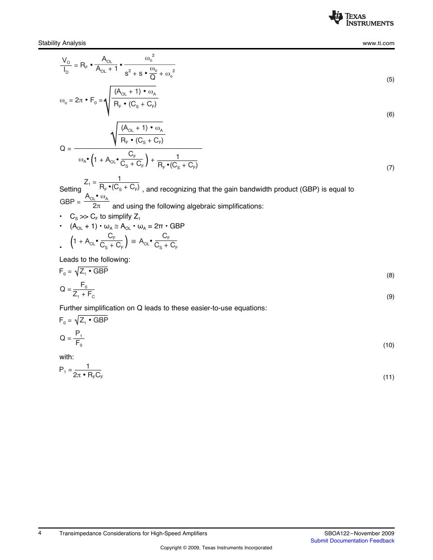
We can use this last point to calculate the maximum achievable bandwidth for a few selected amplifiers.
The OPA847 is a 3.9GHz GBP amplifier with 0.85nV/√Hz input voltage noise. The OPA846 has a
1.75GHz GBP with a 1.2nV/√Hz input voltage noise. The OPA843 is a 800MHz GBP device with a
2nV/√Hz input voltage noise. All three amplifiers—OPA847, OPA846 and OPA843—are bipolar amplifiers.
Finally, the OPA657 is a 1.65GHz GBP device with a 4.8nV/√Hz input voltage noise. Unlike the other
three devices, the OPA657 is a FET input amplifier.
Figure 3 shows an example of achievable bandwidth versus transimpedance gain for a 10pF source
capacitance for various amplifiers.
Figure 3. Maximum Achievable Bandwidth for Selected Op Amps (10pF Source Capacitance)
The relative performance for each amplifier is maintained as the source capacitance varies. Note that the
source capacitance in this example considers the amplifier parasitic, both common-mode and differential
capacitance. When multiple amplifiers can be selected to meet the desired performance—for example, for
RF = 20kΩ, f–3dB = 10MHz—other considerations such as noise or power dissipation must be considered
before making the amplifier selection.
At first glance, using a FET input amplifier does not present any advantages and has one major
inconvenience: its high input voltage noise. The noise analysis will be developed next and then the relative
performance of bipolar technology will be compared with FET technology.
SBOA122– November 2009
Submit Documentation Feedback
Transimpedance Considerations for High-Speed Amplifiers
5
Copyright © 2009, Texas Instruments Incorporated
GBP = 2FRCp-3dBFS··2300250200150100500Maximum AchievableFlat Frequency Response (MHz)1251020501002005001000Maximum Transimpedance Gain (k)WOPA847OPA846OPA657OPA843�
Noise Considerations
www.ti.com
4
Noise Considerations
The equivalent input current noise for a transimpedance amplifier makes the following assumptions:
• This evaluation is an integrated noise analysis that uses spot noise over frequency, and is not intended
to be used as a spot noise equation for narrowband applications.
• The application is dc-coupled, pulse-oriented where the integrated noise is of interest.
• The final signal bandwidth for both the transimpedance design and any post-filtering is greater than 10
times the 1/f noise corner frequency of any of the amplifier noise terms. This consideration allows
those effects to be neglected.
• The transimpedance bandwidth is set greater than the post-filtering.
• The current noise term on the noninverting is either negligible or made negligible by providing
adequate bypassing.
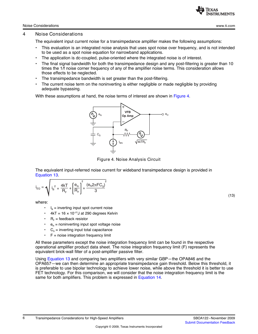
With these assumptions at hand, the noise terms of interest are shown in Figure 4.
Figure 4. Noise Analysis Circuit
The equivalent input-referred noise current for wideband transimpedance design is provided in
Equation 13.
where:
(13)
IB = inverting input spot current noise
4kT = 16 × 10–21J at 290 degrees Kelvin
•
•
• RF = feedback resistor
•
• CS = inverting input total capacitance
•
F = noise integration frequency limit
eN = noninverting input spot voltage noise
All these parameters except the noise integration frequency limit can be found in the respective
operational amplifier product data sheet. The noise integration frequency limit (F) represents the
equivalent brick-wall filter of a post-amplifier passive filter.
Using Equation 13 and comparing two amplifiers with very similar GBP—the OPA846 and the
OPA657—we can then determine an appropriate transimpedance gain threshold. Below this threshold, it
is preferable to use bipolar technology to achieve lower noise, while above the threshold it is better to use
FET technology. For this comparison, we will consider that the noise integration frequency limit is the
same for both amplifiers. This problem is expressed in Equation 14.
6
Transimpedance Considerations for High-Speed Amplifiers
SBOA122– November 2009
Submit Documentation Feedback
Copyright © 2009, Texas Instruments Incorporated
eNeORF4kTRFVFBOp AmpIBNCSi=EQ++eRNF224kTRFiB+2(eN2FC)3pS�
www.ti.com
Example
The solution for RF is shown in Equation 15.
(14)
(15)
For example, with a band-limit filter bandwidth set at 10MHz and a 10pF diode capacitance, all other
parameters are set according to Table 1 (taken from the OPA657 and OPA846 product data sheets).
Device
OPA657
OPA846
Table 1. Device Performance Comparison
Element Specifications
eN(FET) = 4.8nV/√Hz
IB(FET) = 1.3fA/√Hz
CS(FET) = 10pF + 5.2pF = 15.2pF
eN(BIP) = 1.2nV/√Hz
IB(BIP) = 2.8pA/√Hz
CS(BIP) = 10pF + 3.8pF = 13.8pF
The result is that for a resistor lower than 2kΩ, the bipolar amplifier offers a noise advantage; we can
therefore conclude that even though the voltage noise of the OPA657 is high, the total input-referred noise
generated by the OPA657 FET amplifier will be lower than that of the OPA846 bipolar amplifier for any
transimpedance gain greater than 2kΩ. If a larger post-amplifier filter bandwidth is necessary, the bipolar
amplifier (such as the OPA846) will have the lowest noise contribution independent of the resistor.
In general (and from a noise perspective), FET input amplifiers such as the OPA657 are best for large or
very large transimpedance gain with low-to-medium bandwidth because of the post-amplifier filter
limitations, whereas bipolar amplifiers such as the OPA846 are best for medium-to-large transimpedance
gain applications with high bandwidth as limited by the post-amplifier filter.
5
Example
From Figure 3, the maximum achievable bandwidth versus transimpedance gain, it is difficult to separate
the OPA846 from the OPA657 simply by achievable bandwidth. In order to help assess the behavioral
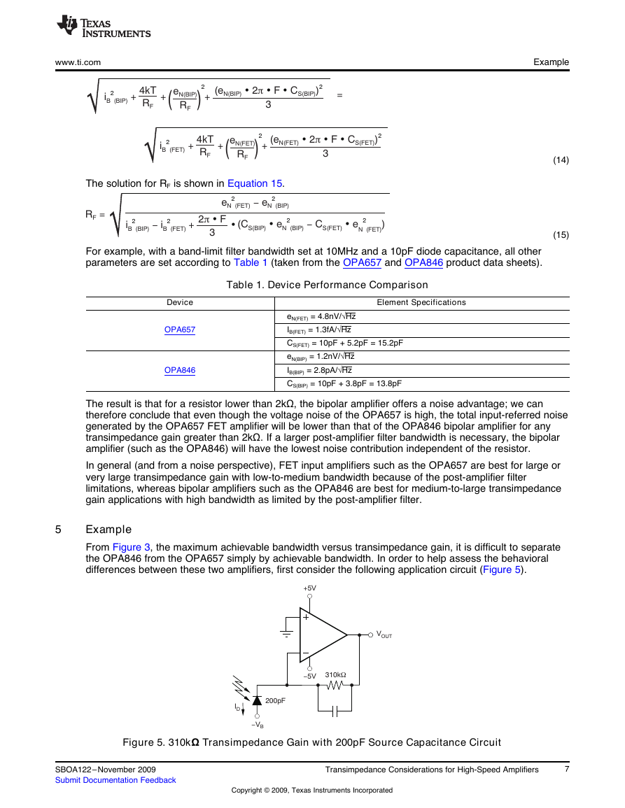
differences between these two amplifiers, first consider the following application circuit (Figure 5).
Figure 5. 310kΩ Transimpedance Gain with 200pF Source Capacitance Circuit
SBOA122– November 2009
Submit Documentation Feedback
Transimpedance Considerations for High-Speed Amplifiers
7
Copyright © 2009, Texas Instruments Incorporated
i+B(BIP)2++(e2FC)3pN(BIP)S(BIP)···24kTRFeRN(BIP)F((2i+B(FET)2++(e2FC)3pN(FET)S(FET)···24kTRFeRN(FET)F((2=RF=eeN(FET)N(BIP)-22+2F3p·iiB(BIP)B(FET)-22·(CeCe)-S(BIP)(BIP)S(FET)(FET)NN··22+5VVOUT-5V310kW200pF-VBID�
DC-Parameters Consideration
www.ti.com
In this circuit, using Equation 12, the OPA846 achieves 2.1MHz while the OPA657 achieves 2MHz,
making them equivalent on that specification. Looking at the noise, the OPA657 yields a 5pA/√Hz
equivalent input noise current if we assume the noise power bandwidth limit is set at 1.4MHz. This noise is
dominated by the third term of the total noise equation, which is the effect of the rising portion of the noise
gain curve times the relatively high 4.8nV/√Hz input voltage noise for the OPA657. The OPA846, which
has a much lower voltage noise but much higher current noise, actually yielded a lower equivalent input
noise current of 3pA/√Hz. So why is the OPA846 not used in this application?
6
DC-Parameters Consideration
The input bias current of the OPA846, 19μA, generates an output offset voltage with the feedback resistor
of 310kΩ of 5.89V. Because the OPA846 is operating on a ±5V power supply, this offset voltage sends
the output into saturation. Adding a 310kΩ resistor on the noninverting input allows bias current
cancellation but now puts 5.89V common-mode voltage on the input, exceeding the common-mode input
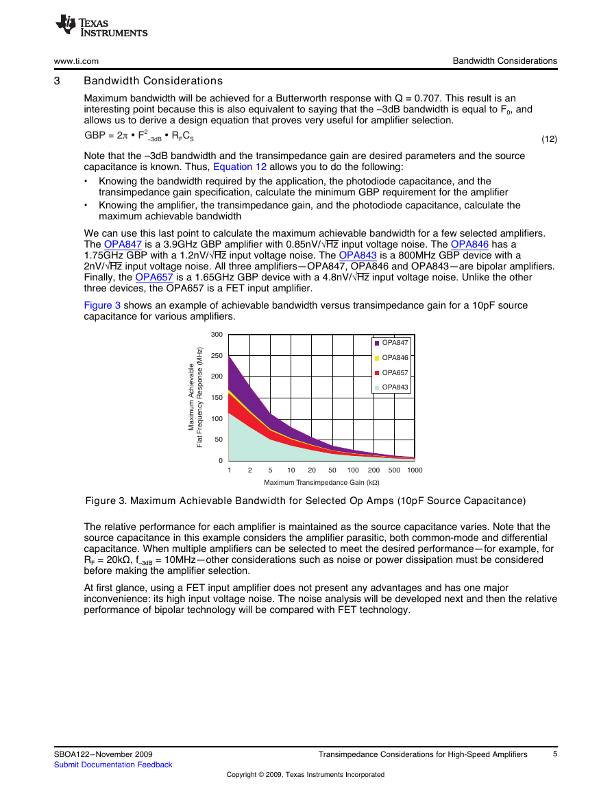
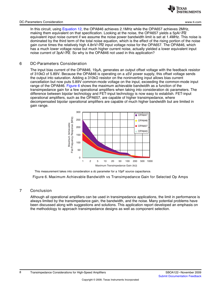
range of the OPA846. Figure 6 shows the maximum achievable bandwidth as a function of the
transimpedance gain for a few operational amplifiers when taking into consideration dc parameters. The
difference between bipolar technology and FET-input technology is now easy to establish. FET-input
operational amplifiers, such as the OPA657, are capable of higher transimpedance, where
decompensated bipolar operational amplifiers are capable of much higher bandwidth but are limited in
gain range.
This measurement takes into consideration a dc parameter for a 10pF source capacitance.
Figure 6. Maximum Achievable Bandwidth vs Transimpedance Gain for Selected Op Amps
7
Conclusion
Although all operational amplifiers can be used in transimpedance applications, the limit in performance is
always limited by the transimpedance gain, the bandwidth, and the noise. Many potential problems have
been discussed along with suggestions and solutions. This application report developed an emphasis on
the methodology to approach transimpedance designs as well as component selection.
8
Transimpedance Considerations for High-Speed Amplifiers
SBOA122– November 2009
Submit Documentation Feedback
Copyright © 2009, Texas Instruments Incorporated
300250200150100500Maximum AchievableFlat Frequency Response (MHz)1251020501002005001000Maximum Transimpedance Gain (k)WOPA847OPA846OPA657OPA843�



 2023年江西萍乡中考道德与法治真题及答案.doc
 2012年重庆南川中考生物真题及答案.doc
 2013年江西师范大学地理学综合及文艺理论基础考研真题.doc
 2020年四川甘孜小升初语文真题及答案I卷.doc
 2020年注册岩土工程师专业基础考试真题及答案.doc
 2023-2024学年福建省厦门市九年级上学期数学月考试题及答案.doc
 2021-2022学年辽宁省沈阳市大东区九年级上学期语文期末试题及答案.doc
 2022-2023学年北京东城区初三第一学期物理期末试卷及答案.doc
 2018上半年江西教师资格初中地理学科知识与教学能力真题及答案.doc
 2012年河北国家公务员申论考试真题及答案-省级.doc
 2020-2021学年江苏省扬州市江都区邵樊片九年级上学期数学第一次质量检测试题及答案.doc
 2022下半年黑龙江教师资格证中学综合素质真题及答案.doc